

Winbond Electronics W83194R-39A, W83194R-39 Datasheet

W83194R-39/-39A
100MHZ 3-DIMM CLOCK
1.0 GENERAL DESCRIPTION
The W83194R-39/-39A is a Clock Synthesizer which provides all clocks required for high-speed RISC
or CISC microprocessor such as Intel Pentium II. W83194R-39 provides eight different frequency of
CPU and PCI clocks and W83194R-39A provides sixteen CPU/PCI frequencies which are externally
selectable with smooth transitions. W83194R-39/-39A also provides 13 SDRAM clocks controlled by
the none-delay buffer_in pin.
The W83194R-39/-39A accepts a 14.318 MHz reference crystal as its input and runs on a 3.3V
supply. Spread spectrum built in at ¡Ó0.5% or ¡Ó0.25% to reduce EMI. Programmable stopping
individual clock outputs and frequency selection through I2C interface. The device meets the
Pentium power-up stabilization, which requires CPU and PCI clocks be stable within 2 ms after
power-up. It is not recommend to use the dual function pin for the slots(ISA, PCI, CPU, DIMM). The
add on cards may have a pull up or pull down.
High drive six PCI and thirteen SDRAM CLOCK outputs typically provide greater than 1 V /ns slew
rate into 30 pF loads. Two CPU CLOCK outputs typically provide better than 1 V /ns slew rate into 20
pF loads as maintaining 50¡Ó 5% duty cycle. The fixed frequency outputs as REF, 24MHz, and 48
MHz provide better than 0.5V /ns slew rate.
2.0 PRODUCT FEATURES
• Supports Pentium II CPU with I2C.
• 2 CPU clocks (one free-running CPU clock)
• 13 SDRAM clocks for 3 DIMs
• 6 PCI synchronous clocks
• One IOAPIC clock for multiprocessor support
• Optional single or mixed supply:
(Vddq1=Vddq2 = Vddq3 = Vddq4 = VddL1 =VddL2= 3.3V) or (Vddq1= Vddq2 = Vddq3=Vddq4 =
3.3V, VddL1 = VdqL2 = 2.5V)
• < 250ps skew among CPU and SDRAM clocks
• < 250ps skew among PCI clocks
• < 5ns propagation delay SDRAM from buffer input
• Skew from CPU(earlier) to PCI clock -1 to 4ns, center 2.6ns.
• Smooth frequency switch with selections from 50 MHz to 133 MHz CPU
• I2C 2-Wire serial interface and I2C read back
Publication Release Date: May 1998
- 1 - Revision 0.20
W83194R-39/-39A
W83194R-39
W83194R-39A
• ¡Ó0.25% or ¡Ó0.5% spread spectrum function to reduce EMI
• Programmable registers to enable/stop each output and select modes
(mode as Tri-state or Normal )
• 2ms power up clock stable time
• MODE pin for power Management
• One 48 MHz for USB & one 24 MHz for super I/O
• 48-pin SSOP package
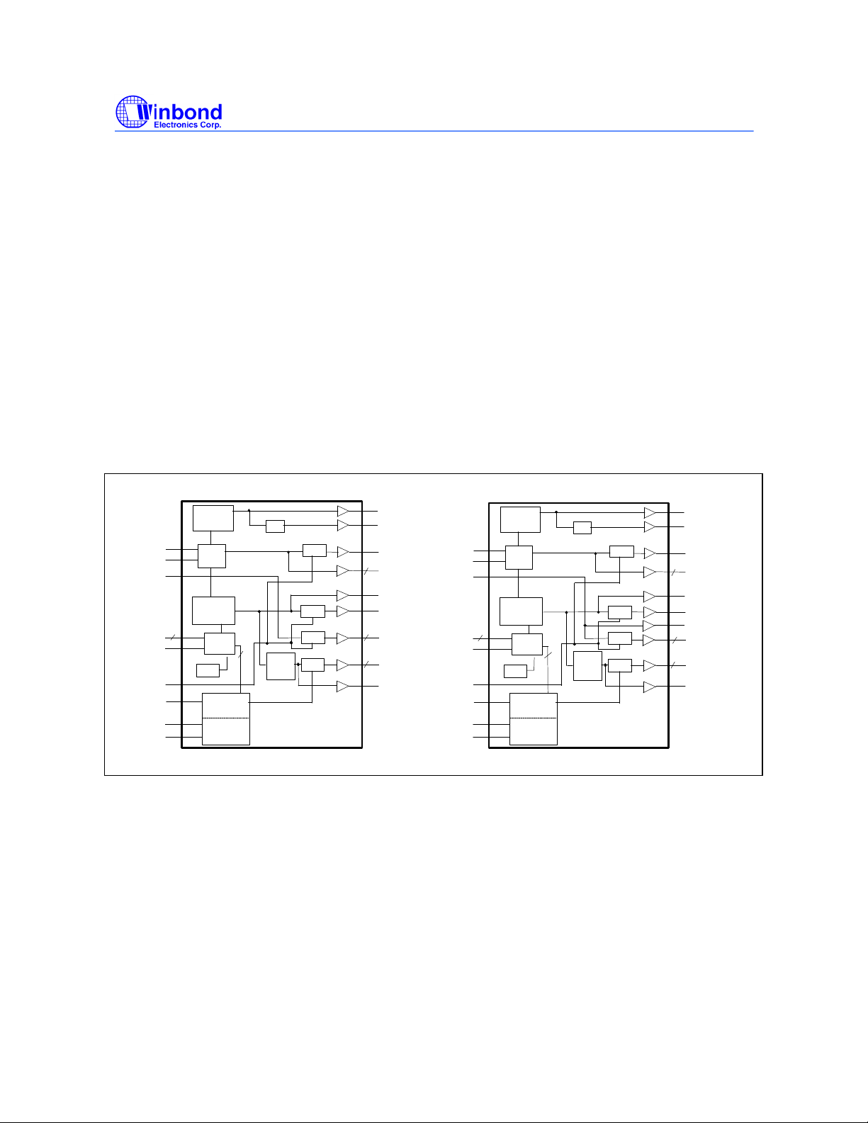
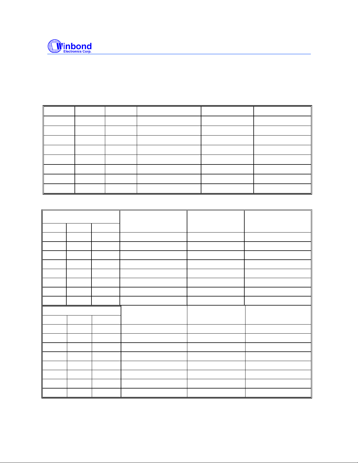
3.0 BLOCK DIAGRAM
PRELIMINARY
BUFFER IN
CPU_STOP#
PCI_STOP#
Xin
Xout
FS(0:2)*
MODE*
SDATA*
SDCLK*
PLL2
~
XTAL
OSC
6
PLL1
Spread
Spectrum
3
LATCH
~
POR
Control
Logic
Config.
Reg.
1/2
STOP
STOP
STOP
4
PCI
STOP
Clock
Divider
48MHz
24MHz
IOAPIC
REF(0:1)
2
CPUCLK_F
CPUCLK1
SDRAM(0:12)
13
PCICLK(0:4)
5
PCICLK_F
Xin
Xout
BUFFER IN
FS(0:3)*
MODE*
CPU_STOP#
PCI_STOP#
SDATA*
SDCLK*
PLL2
~
XTAL
OSC
6
PLL1
Spread
Spectrum
4
LATCH
~
POR
Control
Logic
Config.
Reg.
1/2
STOP
STOP
STOP
4
PCI
STOP
Clock
Divider
48MHz
24MHz
IOAPIC
REF(0:1)
2
CPUCLK_F
CPUCLK1
SDRAM12
SDRAM(0:11)
12
PCICLK(0:4)
5
PCICLK_F
Publication Release Date: May 1998
- 2 - Revision 0.20
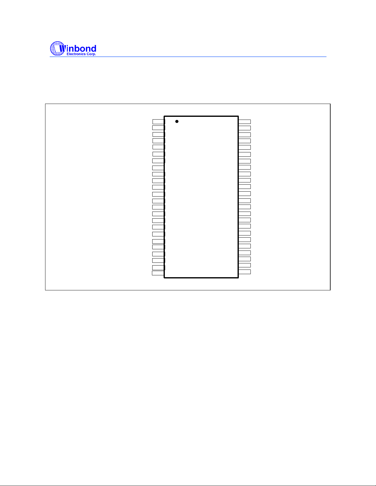
4.0 PIN CONFIGURATION
W83194R-39/-39A
PRELIMINARY
(W83194R-39A )
Vddq1
PCI_STOP#/REF0
Vss
Xin
Xout
Vddq2
PCICLK_F/MODE*
PCICLK0/FS3*
Vss
PCICLK1
PCICLK2
PCICLK3
PCICLK4
Vddq2
BUFFER IN
Vss
SDRAM11
SDRAM10
Vddq3
SDRAM 9
SDRAM 8
Vss
SDATA
SDCLK
1
2
3
4
5
6
7
8
9
10
11
12
13
14
15
16
17
18
19
20
21
22
23
24
48
47
46
45
44
43
42
41
40
39
38
37
36
35
34
33
32
31
30
29
28
27
26
25
VddL1
IOAPIC
REF1/FS2*
Vss
CPUCLK_F
CPUCLK1
VddL2
CPU_STOP#
SDRAM12
Vss
SDRAM 0
SDRAM 1
Vddq3
SDRAM 2
SDRAM 3
Vss
SDRAM 4
SDRAM 5
Vddq3
SDRAM 6
SDRAM 7
Vddq4
48MHz/FS0*
24MHz/FS1*
5.0 PIN DESCRIPTION
IN - Input
OUT - Output
I/O - Bi-directional Pin
# - Active Low
* - Internal 250kΩ pull-up
Publication Release Date: May 1998
- 3 - Revision 0.20
W83194R-39/-39A
PRELIMINARY
5.1 Crystal I/O
SYMBOL PIN I/O FUNCTION
Xin 4 IN Crystal input with internal loading capacitors and
feedback resistors.
Xout 5 OUT Crystal output at 14.318MHz nominally.
5.2 CPU, SDRAM, PCI, IOAPIC Clock Outputs
SYMBOL PIN I/O FUNCTION
CPUCLK_F 44 OUT Free running CPU clock. Not affected by
CPU_STOP#
CPUCLK1 43 OUT Low skew (< 250ps) clock outputs for host
frequencies such as CPU, Chipset and Cache.
Powered by VddL2. Low if CPU_STOP# is low.
CPU_STOP# 41 IN This asynchronous input halts CPUCLK1,IOAPIC &
SDRAM(0:12) at logic
IOAPIC 47 OUT High drive buffered output of the crystal, and is
powered by VddL1.
SDRAM [ 0:12] 17,18,20,21,28
,29,31,32,34,
35,37,38,40
PCICLK_F/
*MODE
PCICLK0/*FS3
(W83194R-39A)
PCICLK [ 0:4 ]
(W83194R-39)
BUFFER IN 15 IN Inputs to fanout for SDRAM outputs.
SDRAM [ 0: 11 ] 17,18,20,21,
7 I/O Free running PCI clock during normal operation.
8 I/O Low skew (< 250ps) PCI clock outputs.
8,10,11,12,13 OUT Low skew (< 250ps) PCI clock outputs. Synchronous
28,29,31,32,
34,35,37,38
OUT SDRAM clock outputs. Fanout buffer outputs from
BUFFER IN pin.(Controlled by chipset)
Latched Input. Mode=1, Pin 2 is REF0; Mode=0,
Pin2 is PCI_STOP#
Latched input for FS3 at initial power up for H/W
selecting the output frequency of CPU, SDRAM and
PCI clocks.
to CPU clocks with 1-48ns skew(CPU early).
O Synchronous DRAM DIMs clocks which have the
same frequency as CPU clocks
“0”
level when driven low.
Publication Release Date: May 1998
- 4 - Revision 0.20
W83194R-39/-39A
PRELIMINARY
5.3 I2C Control Interface
SYMBOL PIN I/O FUNCTION
SDATA 23 I/O Serial data of I2C 2-wire control interface with internal
pull-up resistor.
SDCLK 24 IN Serial clock of I2C 2-wire control interface with
internal pull-up resistor.
5.4 Fixed Frequency Outputs
SYMBOL PIN I/O FUNCTION
REF0 / PCI_STOP# 2 I/O 14.318MHz reference clock. This REF output is the
stronger buffer for ISA bus loads.
Halt PCICLK(0:4) clocks at logic 0 level, when input
low (In mobile mode. MODE=0)
REF1 / *FS2 46 I/O 14.318MHz reference clock.
Latched input for FS2 at initial power up for H/W
selecting the output frequency of CPU, SDRAM and
PCI clocks.
24MHz / *FS1 25 I/O 24MHz output clock.
Latched input for FS1 at initial power up for H/W
selecting the output frequency of CPU, SDRAM and
PCI clocks.
48MHz / *FS0 26 I/O 48MHz output for USB during normal operation.
Latched input for FS0 at initial power up for H/W
selecting the output frequency of CPU, SDRAM and
PCI clocks.
5.5 Power Pins
SYMBOL PIN FUNCTION
Vddq1 1 Power supply for Ref [0:1] crystal and core logic.
VddL1 48 Power supply for IOAPIC output, either 2.5V or 3.3V.
VddL2 42 Power supply for CPUCLK[0:3], either 2.5V or 3.3V.
Vddq2 6, 14 Power supply for PCICLK_F, PCICLK[0:4], 3.3V.
Vddq3 19, 30, 36 Power supply for SDRAM[0:12], and CPU PLL core,
nominal 3.3V.
Vddq4 27 Power for 24 & 48MHz output buffers and fixed PLL
core.
Vss 3,9,16,22,33,39,45 Circuit Ground.
Publication Release Date: May 1998
- 5 - Revision 0.20
W83194R-39/-39A
PRELIMINARY
6.0 FREQUENCY SELECTION
6.1 Frequency table of W83194R-39
FS2 FS1 FS0 CPU,SDRAM (MHz) PCI (MHz) REF,IOAPIC (MHz)
0 0 0 50 25(CPU/2) 14.318
0 0 1 75 37.5(CPU/2) 14.318
0 1 0 83.3 41.65(CPU/2) 14.318
0 1 1 66.8 33.4(CPU/2) 14.318
1 0 0 103 34.3(CPU/3) 14.318
1 0 1 112 37.33(CPU/3) 14.318
1 1 0 133 33.25(CPU/4) 14.318
1 1 1 100.2 33.3(CPU/3) 14.318
6.2 Frequency table of W83194R-39A
FS3=0 CPU,SDRAM (MHz) PCI (MHz) REF,IOAPIC
FS2 FS1 FS0 (MHz)
0 0 0 124 41.33(CPU/3) 14.318
0 0 1 75 37.5(CPU/2) 14.318
0 1 0 83.3 41.65(CPU/2) 14.318
0 1 1 66.8 33.4(CPU/2) 14.318
1 0 0 103 34.3(CPU/3) 14.318
1 0 1 112 37.33(CPU/3) 14.318
1 1 0 133 44.33(CPU/3) 14.318
1 1 1 100.3 33.3(CPU/3) 14.318
FS3=1 CPU,SDRAM (MHz) PCI (MHz) REF,IOAPIC
FS2 FS1 FS0 (MHz)
0 0 0 120 40.00(CPU/3) 14.318
0 0 1 115 38.33(CPU/3) 14.318
0 1 0 110 36.67(CPU/3) 14.318
0 1 1 105 35.00(CPU/3) 14.318
1 0 0 140 35.00(CPU/4) 14.318
1 0 1 150 37.50(CPU/4) 14.318
1 1 0 124 31.00(CPU/4) 14.318
1 1 1 133 33.25(CPU/4) 14.318
Publication Release Date: May 1998
- 6 - Revision 0.20
W83194R-39/-39A
7.0 MODE PIN -POWER MANAGEMENT INPUT CONTROL
MODE, Pin7 (Latched Input) PIN 2
0 PCI_STOP# (Input)
1 REF0 (Output)
PRELIMINARY
Publication Release Date: May 1998
- 7 - Revision 0.20
 Loading...