

Winbond Electronics W83194R-17A, W83194R-17 Datasheet

W83194R-17/-17A
100MHZ AGP CLOCK FOR SIS CHIPSET
1.0 GENERAL DESCRIPTION
The W83194R-17/-17A is a Clock Synthesizer which provides all clocks required for high-speed RISC
or CISC microprocessor such as Intel PentiumII, PentiumPro , AMD or Cyrix. Eight different
frequency of CPU, AGP and PCI clocks are externally selectable with smooth transitions. The
W83194R-17/-17A provides AGP clocks especially for clone chipset. The highest CPU frequency
provided by the W83194R-17 is up to 100MHz, but the one of W83194R-17A is up to 133MHz.
The W83193R-17/-17A provides I2C serial bus interface to program the registers to enable or disable
each clock outputs and choose the 0.5% or 1.5% center type spread spectrum to reduce EMI.
The W83194R-17/-17A accepts a 14.318 MHz reference crystal as its input and runs on a 3.3V
supply. High drive PCI and SDRAM CLOCK outputs typically provide greater than 1 V /ns slew rate
into 30 pF loads. CPU CLOCK outputs typically provide better than 1 V /ns slew rate into 20 pF loads
as maintaining 50¡Ó 5% duty cycle. The fixed frequency outputs as REF, 24MHz, and 48 MHz
provide better than 0.5V /ns slew rate.
2.0 PRODUCT FEATURES
• Supports Pentium, Pentium Pro, Pentium II, AMD and Cyrix CPUs with I2C.
• 4 CPU clocks
• 12 SDRAM clocks for 3 DIMMs
• Two AGP clocks
• 6 PCI synchronous clocks.
• Optional single or mixed supply:
(Vdd = Vddq3 = Vddq2 = Vddq2b = 3.3V) or (Vdd =Vddq2 = Vddq3 = 3.3V, Vddq2b = 2.5V)
• Skew form CPU to PCI clock -1 to 4 ns, center 2.6 ns, AGP to CPU sync. skew 0 ns (250 ps)
• Smooth frequency switch with selections from 60 MHz to 133 MHz CPU
• I2C 2-Wire serial interface and I2C read back
¡Ó
•
• Programmable registers to enable/stop each output and select modes
(mode as Tri-state or Normal )
• MODE pin for power Management
• 48 MHz for USB
• 24 MHz for super I/O
• 48-pin SSOP package
0.5% or
¡Ó
1.5% center type spread spectrum function to reduce EMI
Publication Release Date: Sep. 1998
- 1 - Revision 0.20
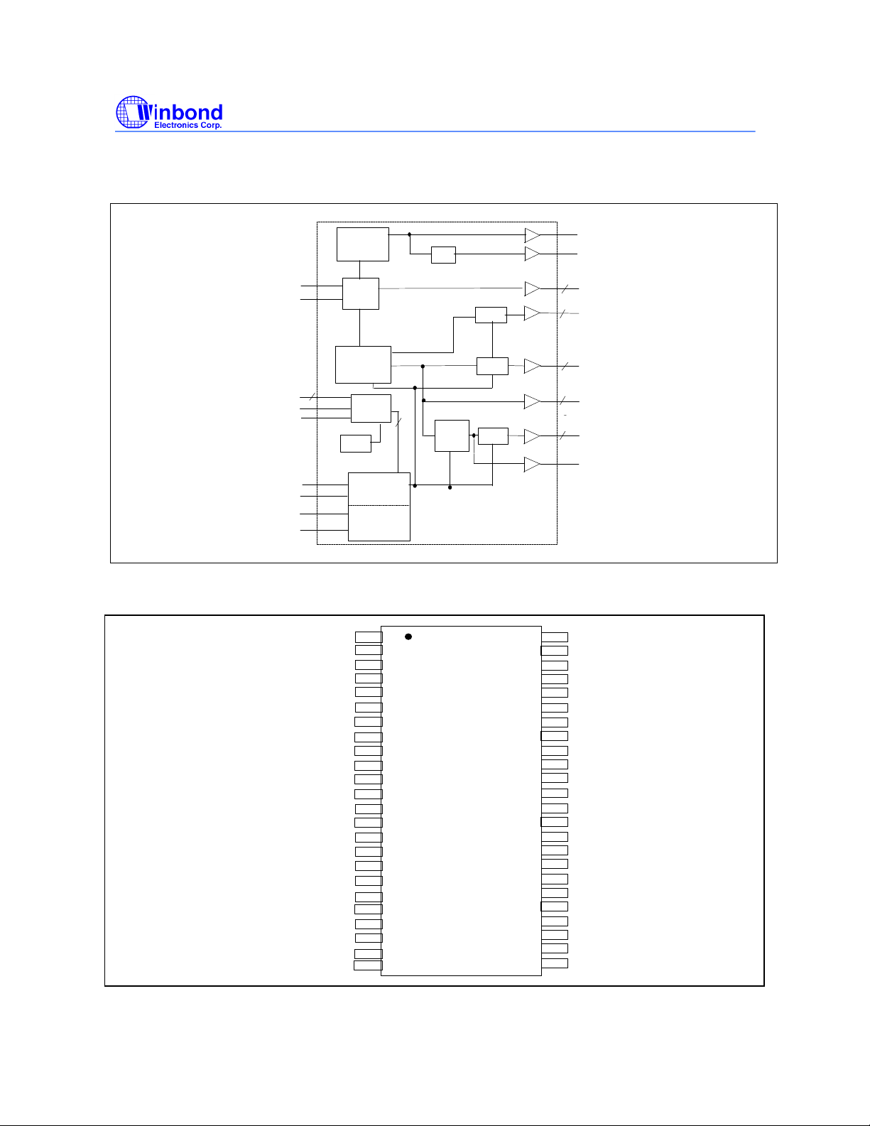
3.0 BLOCK DIAGRAM
W83194R-17/-17A
PRELIMINARY
X1
X2
3
FS(0:2)
MODE
CPU3.3#_2.5
CPU_STOP#
PCI_STOP#
SDATA
SCLK
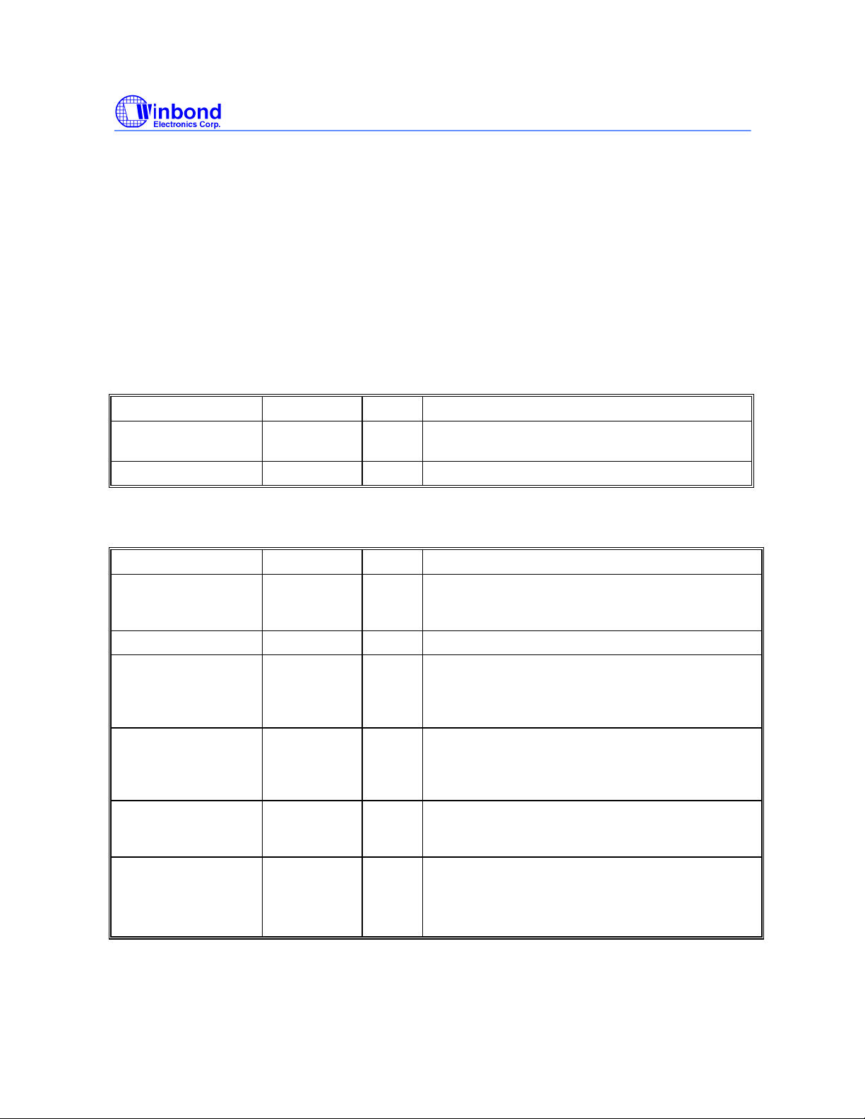
4.0 PIN CONFIGURATION
REF0/CPU3.3#_2.5
Vddq3
PCICLK_F/*FS1
PCICLK0/*FS2
PCICLK1
PCICLK2
PCICLK3
PCICLK4
Vddq3
AGP0
CPU_STOP#/SDRAM11
PCI_STOP#/SDRAM10
Vddq3
SDRAM 9
SDRAM 8
SDATA
SDCLK
Vdd
Vss
Xin
Xout
Vss
Vss
Vss
PLL2
~
XTAL
OSC
PLL1
Spread
Spectrum
LATCH
POR
Control
Logic
Config.
Reg.
~
16
21
1
2
3
4
5
6
7
8
9
10
11
12
13
14
15
17
18
19
20
22
23
24
48MHz
¡Ò
2
STOP
STOP
5
PCI
clock
STOP
Divder
48
47
46
45
44
43
42
41
40
39
38
37
36
35
34
33
32
31
30
29
28
27
26
25
24MHz
REF(0:1)
2
AGP(0:1)
2
CPUCLK(0:3)
4
SDRAM(0:11)
12
PCICLK(0:4)
5
PCICLK_F
Vddq2
AGP1
REF1
Vss
CPUCLK0
CPUCLK1
Vddq2b
CPUCLK2
CPUCLK3
Vss
SDRAM 0
SDRAM 1
Vddq3
SDRAM 2
SDRAM 3
Vss
SDRAM 4
SDRAM 5
Vddq3
SDRAM 6
SDRAM 7
Vss
48MHz/*FS0
24MHz/*MODE
Publication Release Date: Sep. 1998
- 2 - Revision 0.20
W83194R-17/-17A
PRELIMINARY
5.0 PIN DESCRIPTION
IN - Input
OUT - Output
I/O - Bi-directional Pin
# - Active Low
* - Internal 250kΩ pull-up
5.1 Crystal I/O
SYMBOL PIN I/O FUNCTION
Xin 4 IN Crystal input with internal loading capacitors and
feedback resistors.
Xout 5 OUT Crystal output at 14.318MHz nominally.
5.2 CPU, SDRAM, PCI Clock Outputs
SYMBOL PIN I/O FUNCTION
CPUCLK [ 0:3 ] 40,41,43,44 OUT Low skew (< 250ps) clock outputs for host
frequencies such as CPU, Chipset and Cache.
Vddq2b is the supply voltage for these outputs.
AGP[ 0:1] 15,47 OUT Accelerate Graphic Port clock outputs
SDRAM11/
CPU_STOP#
SDRAM10/
PCI_STOP#
SDRAM [ 0:9] 20,21,28,29,31
PCICLK_F/ *FS1 7 I/O Latched input for FS1 at initial power up for H/W
17 I/O If MODE =1 (default), then this pin is a SDRAM
Clock buffered output. If MODE = 0 , then this pin is
CPU_STOP# input used in power management
mode for synchronously stopping the all CPU clocks.
18 I/O If MODE = 1 (default), then this pin is a SDRAM
clock output. If MODE = 0 , then this pin is
PCI_STOP # and used in power management mode
for synchronously stopping the all PCI clocks.
O SDRAM clock outputs which have the same
,32,34,
35,37,38
frequency as CPU clocks.
selecting the output frequency of CPU, SDRAM and
PCI clocks.
Free running PCI clock during normal operation.
Publication Release Date: Sep. 1998
- 3 - Revision 0.20
W83194R-17/-17A
PRELIMINARY
5.2 CPU, SDRAM, PCI Clock Outputs, continued
SYMBOL PIN I/O FUNCTION
PCICLK 0 / *FS2 8 I/O Latched input for FS2 at initial power up for H/W
selecting the output frequency of CPU, SDRAM and
PCI clocks.
PCI clock during normal operation.
PCICLK [ 1:4 ] 10,11,12,13 OUT Low skew (< 250ps) PCI clock outputs.
5.3 I2C Control Interface
SYMBOL PIN I/O FUNCTION
SDATA 23 I/O Serial data of I2C 2-wire control interface
SDCLK 24 IN Serial clock of I2C 2-wire control interface
5.4 Fixed Frequency Outputs
SYMBOL PIN I/O FUNCTION
REF0 / CPU3.3#_2.5 2 I/O
REF1 46 I/O
24MHz / *MODE 25 I/O
48MHz / *FS0 26 I/O
Internal 250kΩ pull-up.
Latched input for CPU3.3#_2.5 at initial power up.
Reference clock during normal operation.
Latched high - Vddq2b = 2.5V
Latched low - Vddq2b = 3.3V
Internal 250kΩ pull-up.
Internal 250kΩ pull-up.
Latched input for MODE at initial power up. 24MHz
output for super I/O during normal operation.
Internal 250kΩ pull-up.
Latched input for FS0 at initial power up for H/W
selecting the output frequency of CPU, SDRAM and
PCI clocks. 48MHz output for USB during normal
operation.
Publication Release Date: Sep. 1998
- 4 - Revision 0.20
W83194R-17/-17A
PRELIMINARY
5.5 Power Pins
SYMBOL PIN FUNCTION
Vdd 1 Power supply for REF0 crystal and core logic.
Vddq2 42 Power supply for AGP1, REF1either 2.5V or 3.3V.
Vddq2b 48 Power supply for CPUCLK[0:3], either 2.5V or 3.3V
Vddq3 6,14,19, 30, 36 Power supply for SDRAM, PCICLK and 48/24MHz
outputs.
Vss 3,9,16,22,27,
33,39,45
Circuit Ground.
6.0 FREQUENCY SELECTION
6.1 W83194R-17 FREQUECY TABLE
FS2 FS1 FS0 CPU,SDRAM
(MHz)
0 0 0 60 30 60 14.318
0 0 1 66.8 33.4 66.8 14.318
0 1 0 68.5 34.25 68.5 14.318
0 1 1 75 37.5 75 14.318
1 0 0 75 32 64 14.318
1 0 1 83.3 33.3 66.6 14.318
1 1 0 90 30 60 14.318
1 1 1 100 33.3 66.6 14.318
6.2 W83194R-17A FREQUECY TABLE
PCI (MHz) AGP (MHz) REF (MHz)
FS2 FS1 FS0 CPU,SDRAM
(MHz)
0 0 0 112 37.3 74.7 14.318
0 0 1 66.8 33.4 66.8 14.318
0 1 0 124 31 62 14.318
0 1 1 75 37.5 75 14.318
1 0 0 133.3 33.3 66.6 14.318
1 0 1 83.3 33.3 66.6 14.318
1 1 0 95.25 31.75 63.5 14.318
1 1 1 100.2 33.4 66.8 14.318
- 5 - Revision 0.20
PCI (MHz) AGP (MHz) REF (MHz)
Publication Release Date: Sep. 1998
7.0 CPU 3.3#_2.5 BUFFER SELECTION
CPU 3.3#_2.5 ( Pin 2 ) Input Level CPU Operate at
1 VDD = 2.5V
0 VDD = 3.3V
W83194R-17/-17A
PRELIMINARY
Publication Release Date: Sep. 1998
- 6 - Revision 0.20
W83194R-17/-17A
PRELIMINARY
8.0 FUNTION DESCRIPTION
8.1 POWER MANAGEMENT FUNCTIONS
All clocks can be individually enabled or disabled via the 2-wire control interface. On power up,
external circuitry should allow 3 ms for the VCO’s to stabilize prior to enabling clock outputs to
assure correct pulse widths. When MODE=0, pins 18 and 17 are inputs (PCI_STOP#),
(CPU_STOP#), when MODE=1, these functions are not available. A particular clock could be
enabled as both the 2-wire serial control interface and one of these pins indicate that it should be
enabled.
The W83194R-17/-17A may be disabled in the low state according to the following table in order to
reduce power consumption. All clocks are stopped in the low state, but maintain a valid high period
on transitions from running to stop. The CPU and PCI clocks transform between running and stop by
waiting for one positive edge on PCICLK_F followed by negative edge on the clock of interest, after
which high levels of the output are either enabled or disabled.
CPU_STOP# PCI_STOP# CPU & AGP PCI OTHER CLKs XTAL & VCOs
0 0 LOW LOW RUNNING RUNNING
0 1 LOW RUNNING RUNNING RUNNING
1 0 RUNNING LOW RUNNING RUNNING
1 1 RUNNING RUNNING RUNNING RUNNING
8.2 2-WIRE I2C CONTROL INTERFACE
The clock generator is a slave I2C component which can be read back the data stored in the latches
for verification. All proceeding bytes must be sent to change one of the control bytes. The 2-wire
control interface allows each clock output individually enabled or disabled. On power up, the
W83194R-17/-17A initializes with default register settings, and then it’s optional to use the 2-wire
control interface.
The SDATA signal only changes when the SDCLK signal is low, and is stable when SDCLK is high
during normal data transfer. There are only two exceptions. One is a high-to-low transition on
SDATA while SDCLK is high used to indicate the beginning of a data transfer cycle. The other is a
low-to-high transition on SDATA while SDCLK is high used to indicate the end of a data transfer
cycle. Data is always sent as complete 8-bit bytes followed by an acknowledge generated.
Byte writing starts with a start condition followed by 7-bit slave address and [1101 0010], command
code checking [0000 0000], and byte count checking. After successful reception of each byte, an
acknowledge (low) on the SDATA wire will be generated by the clock chip. Controller can start to
write to internal I2C registers after the string of data. The sequence order is as follows:
Publication Release Date: Sep. 1998
- 7 - Revision 0.20
 Loading...