

Winbond Electronics W83194BR-730 Datasheet

W83194BR-730
166MHZ CLOCK FOR SIS CHIPSET
1.0 GENERAL DESCRIPTION
The W83194BR-730 is a Clock Synthesizer which provides all clocks required for high-speed RISC or
CISC microprocessor such as AMD K7. W83194BR-730 provides 64 CPU/PCI frequencies which are
selectable with smooth transitions by hardware or software. W83194BR-730 also provides 13 SDRAM
clocks.
The W83194BR-730 provides step-less frequency programming by controlling the VCO freq. and the
programmable PCI clock output divisor ratio. A watch dog timer is quipped and when time out, the
RESET# pin will output 4ms pulse signal.
The W83194BR-730 accepts a 14.318 MHz reference crystal as its input. Spread spectrum built in at
0~-0.5% or ± 0.25% to reduce EMI. Programmable stopping individual clock outputs and frequency
selection through I2C interface. The device meets the Pentium power-up stabilization, which requires
CPU and PCI clocks be stable within 2 ms after power-up. Using dual function pin for the slots(ISA, PCI,
CPU, DIMM) is not recommend.
2.0 PRODUCT FEATURES
•
Supports AMD CPU with I2C.
•
3 CPU clocks (one free-running CPU clock)
•
13 SDRAM clocks for 3 DIMMs
•
6 PCI synchronous clocks
•
2 AGP clocks
•
2 REF clocks as 14.318MHz outputs
•
< 250ps skew among CPU and SDRAM clocks
•
< 250ps skew among PCI clocks
•
Skew from CPU(earlier) to PCI clock 1 to 4ns, center 2.6ns.
• Smooth frequency switch with selections from 66 MHz to 200 MHz CPU
•
Stepless frequency programming by controlling the VCO freq. and the clock output divisor ratio
•
Programmable skew for CPU to SDRAM and CPU to AGP clock outputs
•
I2C 2-Wire serial interface and I2C read back
•
±0.25% or 0~-0.5% spread spectrum function to reduce EMI
•
Programmable registers to enable/stop each output and select modes
•
MODE pin for power Management and RESET# out when system hang
•
One 48 MHz for USB & one 24_48 MHz for super I/O
• 48-pin SSOP package
Publication Release Date: Oct. 2000
- 1 - Revision 0.60
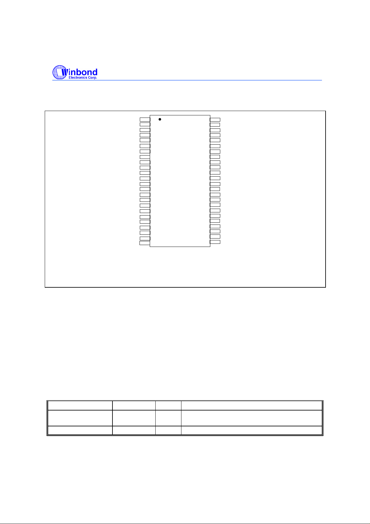
3.0 PIN CONFIGURATION
W83194BR-730
PRELIMINARY
REF1^/ &AGPSEL
PCICLK0^/ &FS1
PCICLK1^/ &FS2
PCICLK5/RESET$
AGPCLK0/SEL24#_48*
AGPCLK1/Mode1*
24_48MHz/&Mode
* : 120K pull-up
&: 120K pull-down
^ : 2X driving stength
$ : Open-drain
#: Active LOW
VddR
REF0^/ &FS3
Vss
Xin
Xout
VddP
PCICLK2^
PCICLK3^
PCICLK4^
Vss
VddAGP
Vss
Vss
48MHz/&FS0
Vdd48
SDATA*
SDCLK*
1
2
3
4
5
6
7
8
9
10
11
12
13
14
15
16
17
18
19
20
21
22
23
24
48
47
46
45
44
43
42
41
40
39
38
37
36
35
34
33
32
31
30
29
28
27
26
25
VddLCPU
CPUC0$
CPUT0$
CPUCS_C1$
Vss
VddSD
SDRAM 0
SDRAM 1
SDRAM 2
Vss
SDRAM 3
SDRAM 4
SDRAM 5
VddSD
SDRAM 6
SDRAM 7
Vss
SDRAM 8/PD#
SDRAM 9/SDRAM_STOP#
VssSD
SDRAM 10/PCI_STOP#
SDRAM11/CPU_STOP#
SDRAM12
VddSD
4.0 PIN DESCRIPTION
IN - Input
OUT - Output
I/O - Bi-directional Pin
# - Active Low
* - Internal 250kΩ pull-up
4.1 Crystal I/O
SYMBOL PIN I/O FUNCTION
Xin 5 IN Crystal input with internal loading capacitors and
feedback resistors.
Xout 6 OUT Crystal output at 14.318MHz nominally.
Publication Release Date:Oct. 2000
- 2 - Revision 0.60

4.2 CPU, SDRAM, PCI, AGP Clock Outputs
SDRAM clock outputs. The same phase as CPUC0$
PCICLK1^/&FS2
SYMBOL PIN I/O FUNCTION
CPUC0$
CPUT0$
CPUCS_C1$ 45 OD Open drain clock for chipset. Stopped if CPU_STOP#
SDRAM [ 0:7],12 42,41,40,38,37
SDRAM 8/PD# 31 OUT Pin21 &Mode=0, SDRAM clock outputs.
SDRAM9/
SDRAM_STOP#
SDRAM 10/
PCI_STOP#
SDRAM 11/
CPU_STOP#
PCICLK0^/&FS1
PCICLK [2:4]^
PCICLK5/
RESET$
AGPCLK0/
SEL24#_48*
AGPCLK1/
Mode1*
47,46 OD Open drain output clock for host frequencies CPU.
,36,34,33, 26
30 OUT Pin21 &Mode=0, SDRAM clock outputs.
28 OUT Pin21 &Mode=0, SDRAM clock outputs.
27 OUT Pin21 &Mode=0, SDRAM clock outputs.
8 I/O Low skew (< 250ps) PCI clock outputs.
9 I/O Low skew (< 250ps) PCI clock outputs.
10,11,12 I/O Low skew (< 250ps) PCI clock outputs.
13 I/O PCI clock during normal operation. (pin 17 MODE1=1)
16 I/O Low skew (< 250ps) AGP clock output.
17 OUT AGP clock outputs
W83194BR-730
PRELIMINARY
Powered by VddLCPU. Stopped if CPU_STOP# is
low.
is low and Register1 bit7=0. The same phase as
CPUC0$.
OUT
Pin21 &Mode=1, PD# input
Pin21 &Mode=1, SDRAM_STOP# input
Pin21 &Mode=1, PCI_STOP# input
Pin21 &Mode=1, CPU_STOP# input
Latched input for FS1 at initial power up for H/W
selecting the output frequency of CPU, SDRAM and
PCI clocks.
Latched input for FS2 at initial power up for H/W
selecting the output frequency of CPU, SDRAM and
PCI clocks.
Latched Input.
If pin17 MODE1=0, RESET# (open drain, 4ms low
active pulse when Watch Dog time out)
Latched Input. SEL24#_48*=1, Pin 21 is 24MHz;
SEL24_48*=0, Pin21 is 48MHz
Latched Input. Mode1*=1, Pin 13 is PCICLK;
Mode1*=0, Pin13 is RESET#
Publication Release Date:Oct. 2000
- 3 - Revision 0.60
W83194BR-730
PRELIMINARY
4.3 I2C Control Interface
SYMBOL PIN I/O FUNCTION
SDATA* 23 I/O Serial data of I2C 2-wire control interface
SDCLK* 24 IN Serial clock of I2C 2-wire control interface
4.4 Fixed Frequency Outputs
SYMBOL PIN I/O FUNCTION
REF0 ^/ &AGPSEL 2 I/O 14.318MHz reference clock. This REF output is the
atched input for &AGPSEL at initial power up for H/W
selecting the output frequency of AGP clocks.
REF1 ^/ &FS3 3 I/O 14.318MHz reference clock.
Latched input for FS3 at initial power up for H/W
selecting the output frequency of CPU, SDRAM and
PCI clocks.
24_48MHz / &Mode 21 I/O 24_48MHz output clock, selected by pin16.
Latched Input. &Mode=0, Pin 27,28,30,31 are SDRAM
clocks; &Mode=0, Pin27,28,29,31 areCPU_STOP#,
SDRAM_STOP#, PCI_STOP#,PD#
48MHz / &FS0 20 I/O 48MHz output for USB during normal operation.
Latched input for FS0 at initial power up for H/W
selecting the output frequency of CPU, SDRAM and
PCI clocks.
4.5 Power Pins
SYMBOL PIN FUNCTION
VddR 1 Power supply for Ref [0:1] crystal and core logic.
VddAGP 15 Power supply for AGP output, 3.3V.
VddLCPU 48 Power supply for CPUC0,T0,CS_C1, either 2.5V or 3.3V.
VddP 7 Power supply for PCICLK[0:5], 3.3V.
VddSD 43,35,29,25 Power supply for SDRAM[0:12], and CPU PLL core,
Vdd48 19 Power for 24 & 48MHz output buffers and fixed PLL core.
Vss 4,14,18,19,29,32,39,44 Circuit Ground.
nominal 3.3V.
Publication Release Date:Oct. 2000
- 4 - Revision 0.60
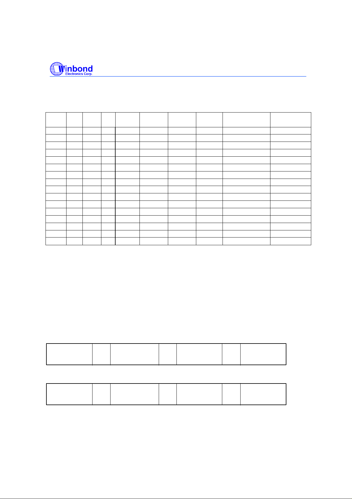
5.0 FREQUENCY SELECTION BY HARDWARE
W83194BR-730
PRELIMINARY
FS3 FS2 FS1 FS0 (MHz) (MHz) (MHz) (MHz) (MHz) (MHz)
0 0 0 0 400 100 100 33.3 66.6 50
VCO CPU SDRAM
PCI AGPSEL=0 AGPSEL=1
0 0 0 1 400 100 133 33.3 66.6 50
0 0 1 0 300 100 150 30.0 60 50
0 0 1 1 400 100 66.6 33.3 66.6 50
0 1 0 0 336 112 112 33.6
67.2 56
0 1 0 1 500 125 100 31.3 62.5 50
0 1 1 0 372 124 124 31 62 46.5
0 1 1 1 400 133 100 33.3 66.6 50
1 0 0 0 400 133 133 33.3 66.6 50
1 0 0 1 300 150 150 30 60 50
1 0 1 0 333 111 166 33.3
1 0 1 1 330 110 165 33.0
66.6 55.6
66 55
1 1 0 0 332 166 166 33.3 66.6 55.6
1 1 0 1 360 90 90 30 60 45
1 1 1 0 192 48 48 32 64 48
1 1 1 1 192 45 60 30 60 45
6.0 SERIAL CONTROL REGISTERS
The Pin column lists the affected pin number and the @PowerUp column gives the default state at true
power up. "Command Code" byte and "Byte Count" byte must be sent following the acknowledge of
the Address Byte. Although the data (bits) in these two bytes are considered "don't care", they must be
sent and will be acknowledge. After that, the sequence described below (Register 0, Register 1,
Register 2, ....) will be valid and acknowledged.
Bytes sequence order for I2C controller :
Clock Address
A(6:0) & R/W
Ack
8 bits dummy
Command code
Ack
8 bits dummy
Byte count
Set R/W to 1 when Read back”, the data sequence is as follows :
Clock Address
A(6:0) & R/W
Ack
Byte 0 Ack
Byte 1
- 5 - Revision 0.60
Ack
Byte0,1,2...
until Stop
Ack
Byte2, 3, 4...
until Stop
Publication Release Date:Oct. 2000
 Loading...