

Winbond Electronics W83194AR-96 Datasheet

W83194AR-96
200MHZ CLOCK FOR WHITNEY CHIPSET
1.0 GENERAL DESCRIPTION
The W83194AR-96 is a Clock Synthesizer for Intel Whitney chipset. W83194AR-96 provides all
clocks required for high-speed RISC or CISC microprocessor and also provides 32 different
frequencies of CPU, SDRAM, PCI, 3V66, IOAPIC clocks frequency setting. All clocks are externally
selectable with smooth transitions.
The W83194AR-96 provides I2C serial bus interface to program the registers to enable or disable
each clock outputs and provides 0.25% center and 0-0.5% down type spread spectrum to reduce EMI.
The W83194AR-96 accepts a 14.318 MHz reference crystal as its input and runs on a 3.3V supply.
High drive PCI and SDRAM CLOCK outputs typically provide greater than 1 V /ns slew rate into 30
pF loads. CPU CLOCK outputs typically provide better than 1 V /ns slew rate into 20 pF loads as
maintaining 50± 5% duty cycle. The fixed frequency outputs as REF, 24MHz, and 48 MHz provide
better than 0.5V /ns slew rate.
1.0 PRODUCT FEATURES
•
2 CPU clocks
•
9 SDRAM clocks for 2 DIMMs
• 8 PCI synchronous clocks.
•
Optional single or mixed supply:
(VDDR = VDDP=VDDS = VDD48 = VDD3 = 3.3V, VDDA=VDDC=2.5V)
•
Skew form CPU to PCI clock -1 to 4 ns, center 2.6 ns
•
Smooth frequency switch with selections from 66.8 to 200MHz
• I2C 2-Wire serial interface and I2C read back
•
0.25% or 0.5% center type spread spectrum
•
Programmable registers to enable/stop each output and select modes
(mode as Tri-state or Normal )
•
48 MHz for USB
•
24 MHz for super I/O
• Packaged in 48-pin SSOP
Publication Release Date: July 1999
- 1 - Revision 0.35
W83194AR-96
PRELIMINARY
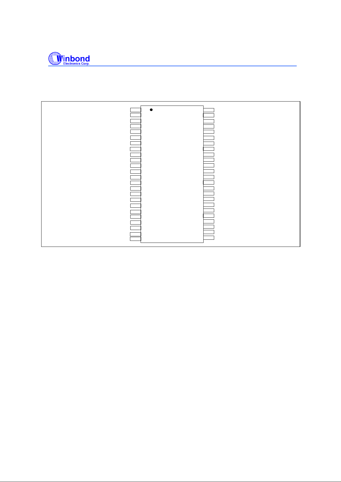
3.0 PIN CONFIGURATION
REF1/*APIC_SEL
VDDR
Xin
Xout
VSS
VSS
3V66-0
3V66-1
VDD3
VDDP
PCICLK0/ FS0#
PCICLK1/ FS1#
PCICLK2/*SEL24_48#
VSS
PCICLK3/ FS4#
PCICLK4
PCICLK5
VDDP
PCICLK6
PCICLK7
VSS
PD#
*SDCLK
*SDATA
16
21
1
2
3
4
5
6
7
8
9
10
11
12
13
14
15
17
18
19
20
22
23
24
48
47
46
45
44
43
42
41
40
39
38
37
36
35
34
33
32
31
30
29
28
27
26
25
VddA
IOAPIC
VDDC
CPUCLK0
CPUCLK1
VSS
VSS
SDRAM 0
SDRAM 1
SDRAM 2
VDDS
SDRAM 3
SDRAM 4
SDRAM 5
VSS
SDRAM 6
SDRAM 7
SDRAM_F
VDDS
VSS
24_48MHz/ FS2#
48MHz-0
48MHz-1/ FS3#
VDD48
Publication Release Date: July 1999
- 2 - Revision 0.35
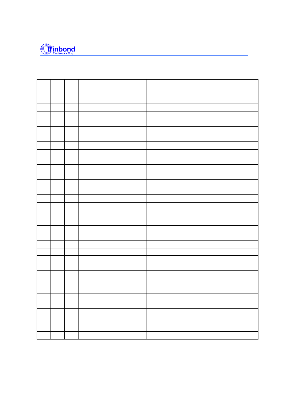
4.0 FREQUENCY SELECTION BY HARDWARE
IOAPIC (MHz)
IOAPIC (MHz)
W83194AR-96
PRELIMINARY
FS4 FS3 FS2 FS1 FS0 CPU
0 0 0 0 0
0 0 0 0 1 90 90 1 60.00 30.00 15.00 30.00
0 0 0 1 0
0 0 0 1 1 72 108 2/3 72.00 36.00 18.00 36.00
0 0 1 0 0
0 0 1 0 1 95.25 95.25 1 63.50 31.75 15.88 31.75
0 0 1 1 0
0 0 1 1 1 124 124 1 82.67 41.33 20.67 41.33
0 1 0 0 0 119 119 1 79.33 39.67 19.83 39.67
0 1 0 0 1 114 114 1 76.00 38.00 19.00 38.00
0 1 0 1 0 110 110 1 73.33 36.67 18.33 36.67
0 1 0 1 1 105 105 1 70.00 35.00 17.50 35.00
0 1 1 0 0
0 1 1 0 1
0 1 1 1 0
0 1 1 1 1
1 0 0 0 0
1 0 0 0 1 125 125 1 83.33 41.67 20.83 41.67
1 0 0 1 0 127 127 1 84.67 42.33 21.17 42.33
1 0 0 1 1 130 130 1 86.67 43.33 21.67 43.33
1 0 1 0 0 140 140 1 70.00 35.00 17.50 35.00
1 0 1 0 1 136 136 1 68.00 34.00 17.00 34.00
1 0 1 1 0 166 166 1 83.00 41.50 20.75 41.50
1 0 1 1 1 155 155 1 77.50 38.75 19.38 38.75
1 1 0 0 0
1 1 0 0 1 117 117 1 78.00 39.00 19.50 39.00
1 1 0 1 0 107 107 1 71.33 35.67 17.83 35.67
1 1 0 1 1 100.9 100.9 1 67.27 33.63 16.82 33.63
1 1 1 0 0
1 1 1 0 1
1 1 1 1 0
1 1 1 1 1
(MHz)
66.8 100.2 2/3
100.2 100.2 1
133.6 133.6 1
133.6 100.2 4/3
83.3 124.95
75 112.5
89.07 133.6 2/3 89.07 44.53 22.27 44.53
121 121 1 80.67 40.33 20.17 40.33
135 101.25 4/3 67.50 33.75 16.88 33.75
150 112.5 4/3 75.00 37.50 18.75 37.50
145 108.75 4/3 72.50
140 105 4/3 70.00
138 103.5 4/3 69.00
137 102.75 4/3 68.50
SDRAM
(MHz)
CPU
/SDRAM
2/3
2/3
3V66 (MHz) PCI(MHz)
66.80 33.40 16.70 33.40
66.80 33.40 16.70 33.40
66.80 33.40 16.70 33.40
66.80 33.40 16.70 33.40
83.30 41.65 20.83 41.65
75.00 37.50 18.75 37.50
36.25 18.13 36.25
35.00 17.50 35.00
34.50 17.25 34.50
34.25 17.13 34.25
APIC_SEL=1
APIC_SEL=0
Publication Release Date: July 1999
- 3 - Revision 0.35
W83194AR-96
PRELIMINARY
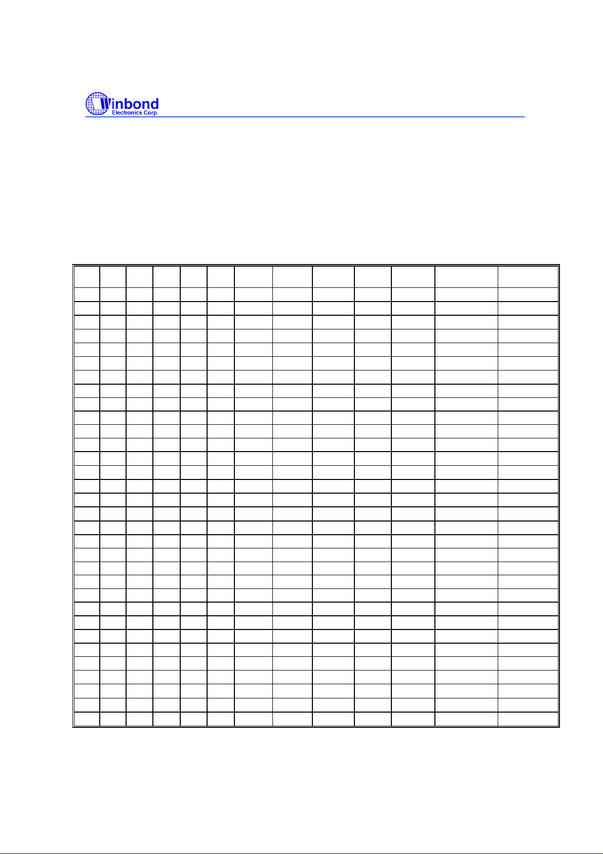
5.0
SERIAL CONTROL 0REGISTERS
The Pin column lists the affected pin number and the @PowerUp column gives the state at true
power up. Registers are set to the values shown only on true power up. "Command Code" byte and
"Byte Count" byte must be sent following the acknowledge of the Address Byte. Although the data
(bits) in these two bytes are considered "don't care", they must be sent and will be acknowledge.
After that, the below described sequence (Register 0, Register 1, Register 2, ....) will be valid and
acknowledged.
Frequency Table Setting by I2C (SEL5 ~ SEL0)
SSE
SS
SS
SS
SS
SS
L5
EL4
EL3
EL2
EL1
EL0
0 0 0 0 0 0
0 0 0 0 0 1 90 90 1 60.00 30.00 15.00 30.00
0 0 0 0 1 0
0 0 0 0 1 1 72 108 2/3 72.00 36.00 18.00 36.00
0 0 0 1 0 0
0 0 0 1 0 1 95.25 95.25 1 63.50 31.75 15.88 31.75
0 0 0 1 1 0
0 0 0 1 1 1 124 124 1 82.67 41.33 20.67 41.33
0 0 1 0 0 0 119 119 1 79.33 39.67 19.83 39.67
0 0 1 0 0 1 114 114 1 76.00 38.00 19.00 38.00
0 0 1 0 1 0 110 110 1 73.33 36.67 18.33 36.67
0 0 1 0 1 1 105 105 1 70.00 35.00 17.50 35.00
0 0 1 1 0 0 83.3 124.95
0 0 1 1 0 1 75 112.5
0 0 1 1 1 0 89.07 133.6 2/3 89.07 44.53 22.27 44.53
0 0 1 1 1 1 121 121 1 80.67 40.33 20.17 40.33
0 1 0 0 0 0
0 1 0 0 0 1 125 125 1 83.33 41.67 20.83 41.67
0 1 0 0 1 0 127 127 1 84.67 42.33 21.17 42.33
0 1 0 0 1 1 130 130 1 86.67 43.33 21.67 43.33
0 1 0 1 0 0 140 140 1 70.00 35.00 17.50 35.00
0 1 0 1 0 1 136 136 1 68.00 34.00 17.00 34.00
0 1 0 1 1 0 166 166 1 83.00 41.50 20.75 41.50
0 1 0 1 1 1 155 155 1 77.50 38.75 19.38 38.75
0 1 1 0 0 0
0 1 1 0 0 1 117 117 1 78.00 39.00 19.50 39.00
0 1 1 0 1 0 107 107 1 71.33 35.67 17.83 35.67
0 1 1 0 1 1 100.9 100.9 1 67.27 33.63 16.82 33.63
0 1 1 1 0 0
0 1 1 1 0 1
0 1 1 1 1 0
0 1 1 1 1 1
CPU
(MHz)
66.8 100.2 2/3
100.2 100.2 1
133.6 133.6 1
133.6 100.2 4/3
135 101.25 4/3 67.50 33.75 16.88 33.75
150 112.5 4/3 75.00 37.50 18.75 37.50
145 108.75 4/3 72.50
140 105 4/3 70.00
138 103.5 4/3 69.00
137 102.75 4/3 68.50
SDRAM
(MHz)
CPU/SD
RAM
2/3
2/3
3V66
(MHz)
66.80 33.40 16.70 33.40
66.80 33.40 16.70 33.40
66.80 33.40 16.70 33.40
66.80 33.40 16.70 33.40
83.30 41.65 20.83 41.65
75.00 37.50 18.75 37.50
PCI
(MHz)
36.25 18.13 36.25
35.00 17.50 35.00
34.50 17.25 34.50
34.25 17.13 34.25
IOAPIC (MHz)
APIC_SEL=1
IOAPIC (MHz)
APIC_SEL=0
Publication Release Date: July 1999
- 4 - Revision 0.35
 Loading...