

Winbond Electronics W83178S Datasheet
Preliminary W83178S
100 MHZ 3-DIMM SDRAM BUFFER
1. GENERAL DESCRIPTION
The W83178S is a 13 outputs SDRAM clock buffer for 3-DIMMs models incorporate with W83196S14 which is the clock synthesizer especially for the 100 MHz models such as Intel BX chipsets. (Refer
the datasheet fo Winbond W83196S-14)
The W83178S receives the clock from chipset by the Buffer_In pin and provides almost zero-delay
(less than 4 nS propagation delay) SDRAM buffer outputs for the 13 SDRAM clocks which are
synchronous with the CPU clock outputs priovided by W83196S-14. The clock skew between any two
clock outputs is less than 250 pS and the output buffer impedance is about 15 ohms.
The W83178S also provides I2C serial bus interface to program the registers to enable or disable
each SDRAM clock outputs.
2. FEATURES
• Supports Intel Pentium II CPUs for BX chipset
• 13 SDRAM clocks for 3-DIMMs
• Clock skew less than 250 pS
• Almost none delay Buffer-in controlling SDRAM clocks(<4 nS propagation delay)
2
• I
C 2-wire serial interface
• Programmable registers to enable/stop each output
• Incorporate with W83196S-14
• Packaged in 28-pin SOP
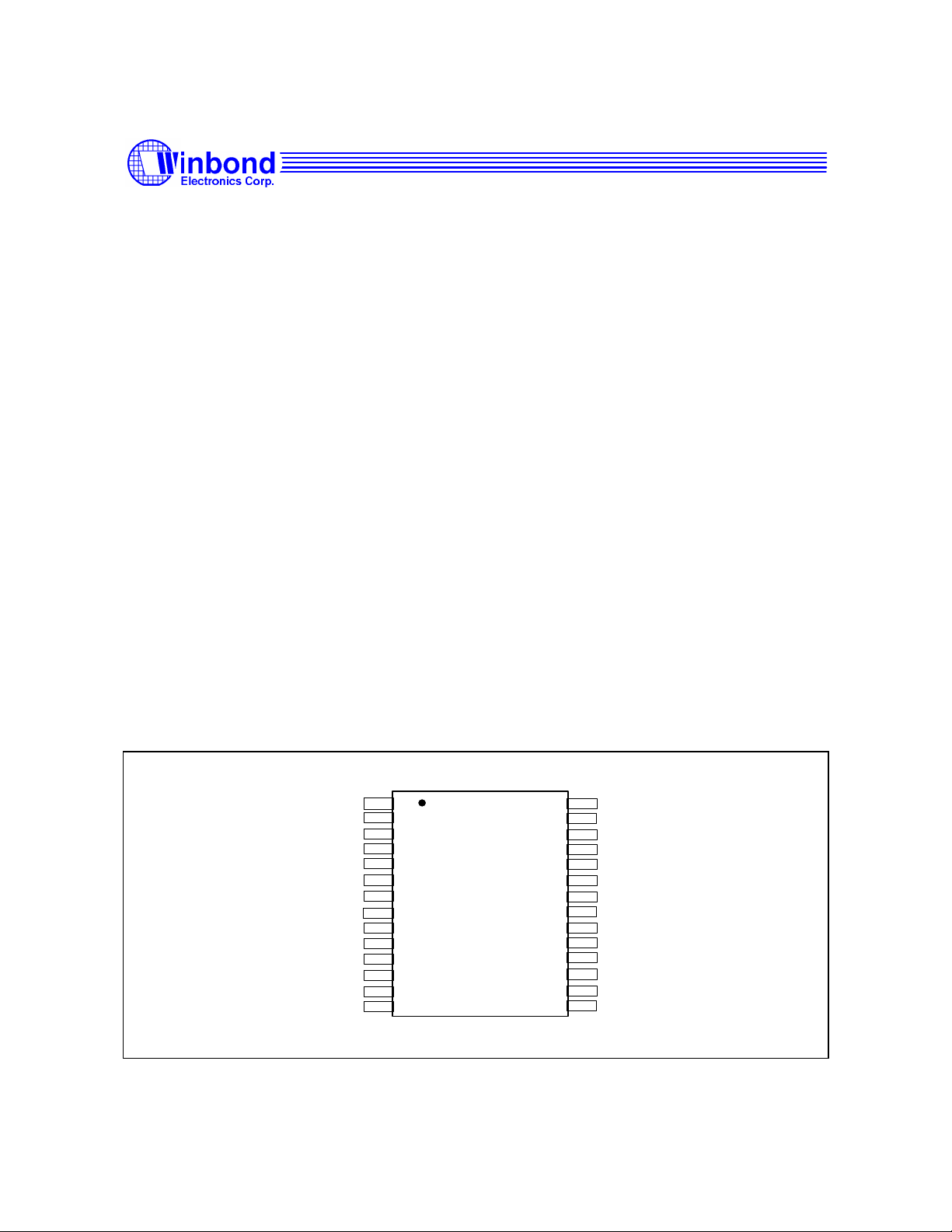
3. PIN CONFIGURATION
VDD
SDRAM 0
SDRAM 1
VDD
SDRAM 2
SDRAM 3
BUFFER_IN
SDRAM 4
SDRAM 5
SDRAM12
VDD
*SDATA
Vss
Vss
1
2
3
4
5
6
7
8
9
10
11
12
13
14
28
27
26
25
24
23
22
21
20
19
18
17
16
15
VDD
SDRAM11
SDRAM10
Vss
VDD
SDRAM 9
SDRAM 8
Vss
VDD
SDRAM 7
SDRAM 6
Vss
Vss
*SCLOCK
Publication Release Date: March 1999
- 1 - Revision A1
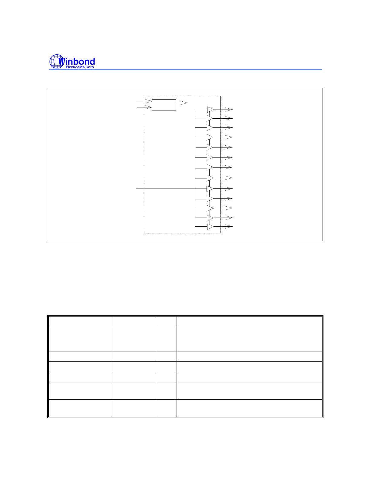
4. BLOCK DIAGRAM
Preliminary W83178S
Buffer_In
5. PIN DESCRIPTION
IN - Input
OUT - Output
I/O - Bi-directional Pin
SDATA
SCLK
Serial port
device Control
SDRAM0
SDRAM1
SDRAM2
SDRAM3
SDRAM4
SDRAM5
SDRAM6
SDRAM7
SDRAM8
SDRAM9
SDRAM10
SDRAM11
SDRAM12
* - Internal 250K Ω pull-up
SYMBOL PIN I/O FUNCTION
SDRAM [ 0:12] 2, 3, 6, 7, 10,
11, 12, 18, 19,
O SDRAM clock outputs which have the same
frequency as CPU clocks.
22, 23, 26, 27
*SDATA 14 I/O Serial data of I2C 2-wire control interface
*SDCLK 15 IN Serial clock of I2C 2-wire control interface
BUFFER_IN 9 IN Clock Input from the chipset
VDD 1, 5, 13, 20,
- Power supply
24, 28
Vss 4, 8, 16, 17,
- Circuit ground
21, 25
- 2 -
Preliminary W83178S
6. FUNCTIONAL DESCRIPTION
6.1 2-Wire I2C Control Interface
The clock generator is a slave I2C component which can be read back the data stored in the latches
for verification. All proceeding bytes must be sent to change one of the control bytes. The 2-wire
control interface allows each clock output individually enabled or disabled. On power up, the
W83178S initializes with default register settings, and then it’optional to use the 2-wire control
interface.
The SDATA signal only changes when the SDCLK signal is low, and is stable when SDCLK is high
during normal data transfer. There are only two exceptions. One is a high-to-low transition on SDATA
while SDCLK is high used to indicate the beginning of a data transfer cycle. The other is a low-tohigh transition on SDATA while SDCLK is high used to indicate the end of a data transfer cycle. Data
is always sent as complete 8-bit bytes followed by an acknowledge generated.
Byte writing starts with a start condition followed by 7-bit slave address and [1101 0010], command
code checking [0000 0000], and byte count checking. After successful reception of each byte, an
acknowledge (low) on the SDATA wire will be generated by the clock chip. Controller can start to
write to internal I2C registers after the string of data. The sequence order is as follows:
Bytes sequence order for I2C controller:
Clock Address
A(6:0) & R/W
Ack
8 bits dummy
Command code
Ack
8 bits dummy
Byte count
Ack
Byte0,1,2...
until Stop
Set R/W to 1 when read back the data sequence is as follows:
Clock Address
A(6:0) & R/W
Ack
Byte 0 Ack
Byte 1
Ack
Byte2, 3, 4...
until Stop
6.2 Serial Control Registers
The Pin column lists the affected pin number and the @PowerUp column gives the state at true
power up. Registers are set to the values shown only on true power up. "Command Code" byte and
"Byte Count" byte must be sent following the acknowledge of the Address Byte. Although the data
(bits) in these two bytes are considered "don't care", they must be sent and will be acknowledge. After
that, the below described sequence (Register 0, Register 1, Register 2, ....) will be valid and
acknowledged.
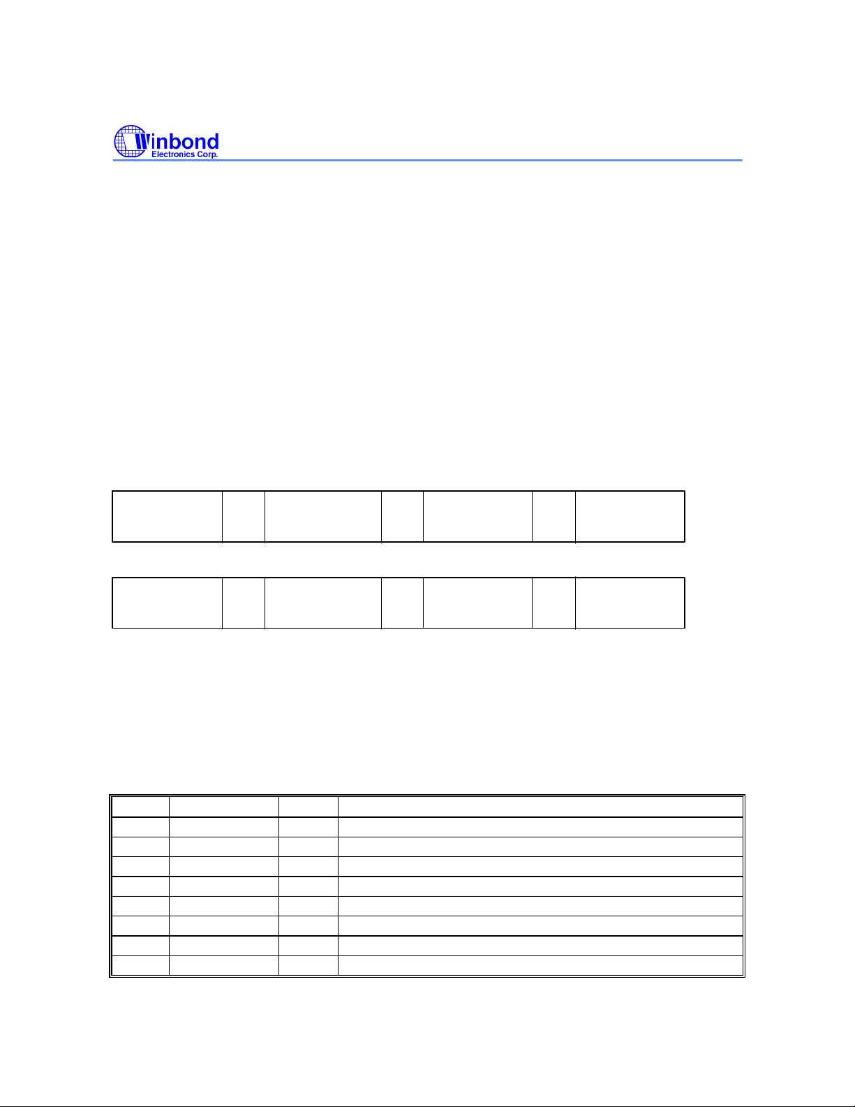
6.2.1 Register 0: (1 = Active, 0 = Inactive)
BIT @POWERUP PIN DESCRIPTION
7 1 11 SDRAM5 (Active/Inactive)
6 1 10 SDRAM4 (Active/Inactive)
5 - - Reserved
4 - - Reserved
3 1 7 SDRAM3 (Active/Inactive)
2 1 6 SDRAM2 (Active/Inactive)
1 1 3 SDRAM1 (Active/Inactive)
0 1 2 SDRAM0 (Active/Inactive)
Publication Release Date: March 1999
- 3 - Revision A1
 Loading...