

Winbond Electronics W79E825ADG, W79E822BSG Datasheet

W79E825A/824A/823B/822B Data Sheet
8-BIT MICROCONTROLLER
Table of Contents-
1 GENERAL DESCRIPTION ......................................................................................................... 4
2 FEATURES ................................................................................................................................. 5
3 PARTS INFORMATION LIST ..................................................................................................... 6
3.1 Lead Free (RoHS) Parts information list......................................................................... 6
4 PIN CONFIGURATION ...............................................................................................................7
5 PIN DESCRIPTION..................................................................................................................... 8
6 FUNCTIONAL DESCRIPTION.................................................................................................... 9
6.1 On-Chip Flash EPROM .................................................................................................. 9
6.2 I/O Ports.......................................................................................................................... 9
6.3 Serial I/O ......................................................................................................................... 9
6.4 Timers ............................................................................................................................. 9
6.5 Interrupts......................................................................................................................... 9
6.6 Data Pointers .................................................................................................................. 9
6.7 Architecture................................................................................................................... 10
6.7.1 ALU ................................................................................................................................10
6.7.2 Accumulator ...................................................................................................................10
6.7.3 B Register.......................................................................................................................10
6.7.4 Program Status Word: ....................................................................................................10
6.7.5 Scratch-pad RAM ...........................................................................................................10
6.7.6 Stack Pointer ..................................................................................................................11
6.8 Power Management...................................................................................................... 11
7 MEMORY ORGANIZATION...................................................................................................... 12
7.1 Program Memory (on-chip Flash) ................................................................................. 12
7.2 Data Memory ................................................................................................................ 12
7.3 Register Map................................................................................................................. 13
7.4 Working Registers......................................................................................................... 16
7.5 Bit addressable Locations............................................................................................. 16
7.6 Stack ............................................................................................................................. 16
8 SPECIAL FUNCTION REGISTERS ......................................................................................... 17
9 INSTRUCTION SET.................................................................................................................. 48
9.1 Instruction Timing.......................................................................................................... 56
10 POWER MANAGEMENT.......................................................................................................... 59
10.1 Idle Mode ...................................................................................................................... 59
10.2 Power Down Mode ....................................................................................................... 59
11 RESET CONDITIONS............................................................................................................... 60
11.1 Sources of reset............................................................................................................ 60
11.1.1 External Reset..............................................................................................................60
Publication Release Date: May 3, 2007
- 1 - Revision A7.1

W79E825A/824A/823B/822B Data Sheet
11.1.2 Power-On Reset (POR)................................................................................................ 60
11.1.3 Watchdog Timer Reset.................................................................................................60
11.2 Reset State ................................................................................................................... 60
12 INTERRUPTS ........................................................................................................................... 63
12.1 Interrupt Sources .......................................................................................................... 63
12.2 Priority Level Structure ................................................................................................. 65
12.3 Response Time............................................................................................................. 66
12.4 Interrupt Inputs.............................................................................................................. 67
13 PROGRAMMABLE TIMERS/COUNTERS ............................................................................... 69
13.1 Timer/Counters 0 & 1.................................................................................................... 69
13.1.1 Time-Base Selection ....................................................................................................69
13.1.2 Mode 0 .........................................................................................................................69
13.1.3 Mode 1 .........................................................................................................................70
13.1.4 Mode 2 .........................................................................................................................71
13.1.5 Mode 3 .........................................................................................................................71
14 NVM MEMORY ......................................................................................................................... 73
15 WATCHDOG TIMER................................................................................................................. 75
15.1 WATCHDOG CONTROL.............................................................................................. 76
15.2 CLOCK CONTROL of Watchdog.................................................................................. 77
16 SERIAL PORT (UART) ............................................................................................................. 78
16.1 MODE 0 ........................................................................................................................ 78
16.2 MODE 1 ........................................................................................................................ 79
16.3 MODE 2 ........................................................................................................................ 81
16.4 MODE 3 ........................................................................................................................ 82
16.5 Framing Error Detection ............................................................................................... 83
16.6 Multiprocessor Communications................................................................................... 83
17 TIME ACCESS PROCTECTION .............................................................................................. 85
18 KEYBOARD INTERRUPT (KBI) ............................................................................................... 87
19 ANALOG COMPARATORS ...................................................................................................... 88
20 I/O PORT CONFIGURATION ................................................................................................... 89
20.1 Quasi-Bidirectional Output Configuration ..................................................................... 89
20.2 Open Drain Output Configuration ................................................................................. 90
20.3 Push-Pull Output Configuration .................................................................................... 91
20.4 Input Only Configuration ............................................................................................... 91
21 OSCILLATOR ........................................................................................................................... 92
21.1 On-Chip RC Oscillator Option....................................................................................... 92
21.2 External Clock Input Option .......................................................................................... 93
21.3 CPU Clock Rate select ................................................................................................. 93
22 POWER MONITORING FUNCTION ........................................................................................ 94
22.1 Power On Detect........................................................................................................... 94
22.2 Brownout Detect ........................................................................................................... 94
23 PULSE-WIDTH-MODULATED (PWM) OUTPUTS................................................................... 95
- 2 -

W79E825A/824A/823B/822B Data Sheet
ANALOG-TO-DIGITAL CONVERTER ...................................................................................... 99
24
24.1 ADC Resolution and Analog Supply:.......................................................................... 100
25 I2C SERIAL CONTROL .......................................................................................................... 102
25.1 SIO Port ...................................................................................................................... 102
25.2 The I2C Control Registers: ......................................................................................... 103
25.2.1 The Address Registers, I2ADDR ................................................................................103
25.2.2 The Data Register, I2DAT ..........................................................................................103
25.2.3 The Control Register, I2CON .....................................................................................104
25.2.4 The Status Register, I2STATUS................................................................................. 104
25.2.5 The I2C Clock Baud Rate Bits, I2CLK ........................................................................ 104
25.3 Modes of Operation .................................................................................................... 105
25.3.1 Master Transmitter Mode ...........................................................................................105
25.3.2 Master Receiver Mode ...............................................................................................105
25.3.3 Slave Receiver Mode .................................................................................................105
25.3.4 Slave Transmitter Mode .............................................................................................106
25.4 Data Transfer Flow in Five Operating Modes............................................................. 106
26 ICP (IN-CIRCUIT PROGRAM) FLASH PROGRAM ............................................................... 112
27 CONFIG BITS ......................................................................................................................... 113
27.1 CONFIG1 .................................................................................................................... 113
27.2 CONFIG2 .................................................................................................................... 114
28 ELECTRICAL CHARACTERISTICS....................................................................................... 116
28.1 Absolute Maximum Ratings ........................................................................................ 116
28.2 DC ELECTRICAL CHARACTERISTICS .................................................................... 117
28.3 The ADC Converter DC ELECTRICAL CHARACTERISTICS ................................... 119
28.4 The COMPARATOR ELECTRICAL CHARACTERISTICS ........................................ 119
28.5 AC ELECTRICAL CHARACTERISTICS .................................................................... 119
28.6 EXTERNAL CLOCK CHARACTERISTICS ................................................................ 120
28.7 AC SPECIFICATION .................................................................................................. 120
28.8 TYPICAL APPLICATION CIRCUITS.......................................................................... 120
29 PACKAGE DIMENSIONS....................................................................................................... 121
29.1 20-pin SO.................................................................................................................... 121
29.2 20-pin DIP ................................................................................................................... 122
30 REVISION HISTORY .............................................................................................................. 123
Publication Release Date: May 3, 2007
- 3 - Revision A7.1

W79E825A/824A/823B/822B Data Sheet
1. GENERAL DESCRIPTION
The W79E825 series are an 8-bit Turbo 51 microcontroller which has an in-system programmable
Flash EPROM which Flash EPROM can program by ICP (In Circuit Program) or by hardware writer.
The instruction set of the W79E825 series are fully compatible with the standard 8052. The W79E825
series contain a 16K/8K/4K/2K bytes of main Flash EPROM; a 256/128 bytes of RAM; 256/128 bytes
NVM Data Flash EPROM; two 8-bit bi-directional, one 2-bit bi-directional and bit-addressable I/O
ports; two 16-bit timer/counters; 4-channel multiplexed 10-bit A/D convert; 4-channel 10-bit PWM; two
serial ports that include a I2C and an enhanced full duplex serial port. These peripherals are
supported by 13 sources four-level interrupt capability. To facilitate programming and verification, the
Flash EPROM inside the W79E825 series allow the program memory to be programmed and read
electronically. Once the code is confirmed, the user can protect the code for security.
- 4 -

W79E825A/824A/823B/822B Data Sheet
2. FEATURES
• Fully static design 8-bit Turbo 51 CMOS microcontroller up to 20MHz when VDD=4.5V to 5.5V,
12MHz when VDD=2.7V to 5.5V
• 16K/8K/4K/2K bytes of AP Flash EPROM, with ICP and external writer programmable mode.
• 256/128 bytes of on-chip RAM.
• 256/128 bytes NVM Data Flash EPROM for customer data storage used and 10K writer cycles.
• Instruction-set compatible with MSC-51.
• On-chip configurable RC oscillator (6MHz)
• Two 8-bit bi-directional and one 2-bit bi-directional ports.
• Two 16-bit timer/counters.
• 13 interrupts source with four levels of priority.
• One enhanced full duplex serial port with framing error detection and automatic address
recognition.
• The 4 outputs mode and TTL/Schmitt trigger selectable Port.
• Programmable Watchdog Timer.
• Four-channel 10-bit PWM (Pulse Width Modulator).
• Four-channel multiplexed with 10-bits A/D convert.
• One I2C communication port (Master / Slave).
• Eight keypad interrupt inputs.
• Two analog comparators.
• Configurable on-chip oscillator.
• LED drive capability (20mA) on all port pins.
• Low Voltage Detect interrupt and reset.
• Development Tools:
- JTAG ICE(In Circuit Emulation) tool
- ICP(In Circuit Programming) writer
• Packages:
- Lead Free (RoHS) DIP 20: W79E825ADG
- Lead Free (RoHS) DIP 20: W79E825ADG
- Lead Free (RoHS) SOP 20: W79E825ASG
- Lead Free (RoHS) DIP 20: W79E824ADG
- Lead Free (RoHS) SOP 20: W79E824ASG
- Lead Free (RoHS) DIP 20: W79E823BDG
- Lead Free (RoHS) SOP 20: W79E823BSG
- Lead Free (RoHS) DIP 20: W79E822BDG
- Lead Free (RoHS) SOP 20: W79E822BSG
Publication Release Date: May 3, 2007
- 5 - Revision A7.1
W79E825A/824A/823B/822B Data Sheet
3. PARTS INFORMATION LIST
3.1 Lead Free (RoHS) Parts information list
PART NO.
W79E825ADG 16KB 256B 256B DIP-20 Pin
W79E825ASG 16KB 256B 256B SOP-20 Pin
W79E824ADG 8KB 256B 256B DIP-20 Pin
W79E824ASG 8KB 256B 256B SOP-20 Pin
W79E823BDG 4KB 128B 128B DIP-20 Pin
W79E823BSG 4KB 128B 128B SOP-20 Pin
W79E822BDG 2KB 128B 128B DIP-20 Pin
W79E822BSG 2KB 128B 128B SOP-20 Pin
Table 3-1: Lead Free (RoHS) Parts information list
EPROM FLASH
SIZE
RAM
NVM FLASH
EPROM
PACKAGE REMARK
- 6 -
W79E825A/824A/823B/822B Data Sheet
4. PIN CONFIGURATION
20 PIN DIP
PWM3/CMP2/P0.0
PWM2/P1.7
PWM1/P1.6
RST/P1.5
VSS
XTAL1/P2.1
XTAL2/CLKOUT/P2.0
INT1/P1.4
SDA/INT0/P1.3
SCL/T0/P1.2
PWM3/CMP2/P0.0
PWM2/P1.7
PWM1/P1.6
RST/P1.5
VSS
XTAL1/P2.1
XTAL2/CLKOUT/P2.0
INT1/P1.4
SDA/INT0/P1.3
SCL/T0/P1.2
1
2
3
4
5
6
7
8
9
10
20
19
18
17
16
15
14
13
12
11
20 PIN SOP
1
2
3
4
5
6
7
8
9
10
Figure 4-1: Pin Configuration
20
19
18
17
16
15
14
13
12
11
P0.1/CIN2B/PWM0
P0.2/CIN2A/BRAKE
P0.3/CIN1B/AD0
P0.4/CIN1A/AD1
P0.5/CMPREF/AD2
VDD
P0.6/CMP1/AD3
P0.7/T1
P1.0/TXD
P1.1/RXD
P0.1/CIN2B/PWM0
P0.2/CIN2A/BRAKE
P0.3/CIN1B/AD0
P0.4/CIN1A/AD1
P0.5/CMPREF/AD2
VDD
P0.6/CMP1/AD3
P0.7/T1
P1.0/TXD
P1.1/RXD
Publication Release Date: May 3, 2007
- 7 - Revision A7.1
W79E825A/824A/823B/822B Data Sheet
5. PIN DESCRIPTION
SYMBOL TYPE DESCRIPTIONS
RESET: A low on this pin for two machine cycles while the oscillator is
STR (P1.5)
I
running resets the device.
XTAL1(P2.1) I/O
XTAL2(P2.0) I/O
VSS P GROUND: Ground potential
VDD P POWER: SUPPLY: Supply voltage for operation.
P0.0−P0.7
P1.0−P1.7
* TYPE: P: power, I: input, O: output, I/O: bi-directional, H: pull-high, L: pull-low, D: open-drain.
Table 5-1: Pin Description
I/O
I/O
CRYSTAL1: This is the crystal oscillator input. This pin may be driven by
an external clock or configurable I/O pin.
CRYSTAL2: This is the crystal oscillator output. It is the inversion of
XTAL1 or configurable I/O pin.
PORT 0: Port 0 is four mode output pin and two mode input. The
P0.3~P0.6 are 4-channel input ports (ADC0-ADC3) for ADC used.
PORT 1: Port 1 is four mode output pin and two mode input. The P1.2
(SCL) and P1.3 (SDA) is only open drain circuit, and P1.5 only input pin.
- 8 -

W79E825A/824A/823B/822B Data Sheet
6. FUNCTIONAL DESCRIPTION
The W79E825 series architecture consist of a 4T 8051 core controller surrounded by various registers,
16K/8K/4K/2K bytes Flash EPROM, 256/128 bytes of RAM, 256/128 bytes NVM Data Flash EPROM,
three general purpose I/O ports, two timer/counters, one serial port, one I2C serial I/O, 4 channel
PWM with 10-bit counter, 4-channel multiplexed with 10-bit ADC analog input, Flash EPROM program
by Writer and ICP.
6.1 On-Chip Flash EPROM
The W79E825 series include one 16K/8K/4K/2K bytes of main Flash EPROM for application program.
A Writer or ICP programming board is required to program the Flash EPROM or NVM Data Flash
EPROM.
This ICP (In-Circuit Programming) feature makes the job easy and efficient when the application’s
firmware needs to be updated frequently. In some applications, the in-circuit programming feature
makes it possible for the end-user to easily update the system firmware without opening the chassis.
6.2 I/O Ports
The W79E825 series have two 8-bit and one 2-bit port, up to 18 I/O pins using on-chip oscillator &
/RST is input only by reset options. All ports can be used as four outputs mode when it may set by
PxM1.y and PxM2.y SFR’s registers, it has strong pull-ups and pull-downs, and does not need any
external pull-ups. Otherwise it can be used as general I/O port as open drain circuit. All ports can be
used bi-directional and these are as I/O ports. These ports are not true I/O, but rather are pseudo-I/O
ports. This is because these ports have strong pull-downs and weak pull-ups.
6.3 Serial I/O
The W79E825 series have one serial port that is functionally similar to the serial port of the original
8032 family. However the serial port on the W79E825 series can operate in different modes in order to
obtain timing similarity as well. The Serial port has the enhanced features of Automatic Address
recognition and Frame Error detection.
6.4 Timers
The W79E825 series have two 16-bit timers that are functionally and similar to the timers of the 8052
family. When used as timers, the user has a choice of 12 or 4 clocks per count that emulates the
timing of the original 8052.
6.5 Interrupts
The Interrupt structure in the W79E825 series is slightly different from that of the standard 8052. Due
to the presence of additional features and peripherals, the number of interrupt sources and vectors
has been increased.
6.6 Data Pointers
The data pointers of W79E825 series are same as 8052 that has dual 16-bit Data Pointers (DPTR) by
setting DPS bit at AUXR1.0. The figure of dual DPTR is as below diagram.
Publication Release Date: May 3, 2007
- 9 - Revision A7.1
W79E825A/824A/823B/822B Data Sheet
AUXR1.0
DPS=0
DPTR
DPS
DPS=1
Figure 6-1: Dual DPTR
DPTR1
6.7 Architecture
The W79E825 series are based on the standard 8052 device. It is built around an 8-bit ALU that uses
internal registers for temporary storage and control of the peripheral devices. It can execute the
standard 8052 instruction set.
6.7.1 ALU
The ALU is the heart of the W79E825 series. It is responsible for the arithmetic and logical functions. It
is also used in decision making, in case of jump instructions, and is also used in calculating jump
addresses. The user cannot directly use the ALU, but the Instruction Decoder reads the op-code,
decodes it, and sequences the data through the ALU and its associated registers to generate the
required result. The ALU mainly uses the ACC which is a special function register (SFR) on the chip.
Another SFR, namely B register is also used in Multiply and Divide instructions. The ALU generates
several status signals which are stored in the Program Status Word register (PSW).
6.7.2 Accumulator
The Accumulator (ACC) is the primary register used in arithmetic, logical and data transfer operations
in the W79E825 series. Since the Accumulator is directly accessible by the CPU, most of the high
speed instructions make use of the ACC as one argument.
6.7.3 B Register
This is an 8-bit register that is used as the second argument in the MUL and DIV instructions. For all
other instructions it can be used simply as a general purpose register.
6.7.4 Program Status Word:
This is an 8-bit SFR that is used to store the status bits of the ALU. It holds the Carry flag, the Auxiliary
Carry flag, General purpose flags, the Register Bank Select, the Overflow flag, and the Parity flag.
6.7.5 Scratch-pad RAM
The W79E825 series have a 256/128 bytes on-chip scratch-pad RAM. These can be used by the user
for temporary storage during program execution. A certain section of this RAM is bit addressable, and
can be directly addressed for this purpose.
- 10 -

W79E825A/824A/823B/822B Data Sheet
6.7.6 Stack Pointer
The W79E825 series have an 8-bit Stack Pointer which points to the top of the Stack. This stack
resides in the Scratch Pad RAM in the W79E825 series. Hence the size of the stack is limited by the
size of this RAM.
6.8 Power Management
Power Management like the standard 8052, the W79E825 series also have the IDLE and POWER
DOWN modes of operation. In the IDLE mode, the clock to the CPU is stopped while the timers, serial
ports and interrupt lock continue to operate. In the POWER DOWN mode, all clocks are stopped and
the chip operation is completely stopped. This is the lowest power consumption state.
Publication Release Date: May 3, 2007
- 11 - Revision A7.1
W79E825A/824A/823B/822B Data Sheet
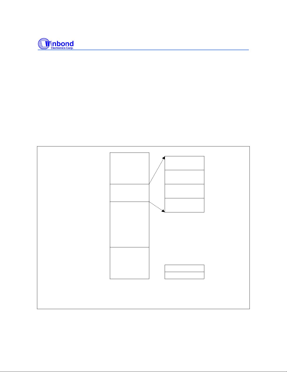
7. MEMORY ORGANIZATION
The W79E825 series separate the memory into two separate sections, the Program Memory and the
Data Memory. The Program Memory is used to store the instruction op-codes, while the Data Memory
is used to store data or for memory mapped devices.
7.1 Program Memory (on-chip Flash)
The Program Memory on the W79E825 series can be up to 16K/8K/4K/2K bytes long. All instructions
are fetched for execution from this memory area. The MOVC instruction can also access this memory
region.
7.2 Data Memory
The NVM Data Memory of Flash EPROM on the W79E825 series can be up to 256/128 bytes long.
The W79E825 series read the content of data memory by using “MOVC A, @A+DPTR”. To write data
is by NVMADDR, NVMDAT and NVMCON SFR’s registers.
FFFFH
FCFFH
FC00H
FBFFH
4000H/2000H
3FFFH/1FFFH
0000H
On-Chip Code Memory Space
Unused
Code Memory
256 Bytes
NVM
Data Mem ory
Unused
Code Memory
16K/8K Bytes
On-Chip
Code Memory
Page 3
64 bytes
Page 2
64 bytes
Page 1
64 bytes
Page 0
64 bytes
FCFFH
FCC0H
FCBFH
FC80H
FC7FH
FC40H
FC3FH
FC00H
NVM Data Memory Area
CONFIG 2
CONFIG 1
Figure 7-1: W79E825/824 Memory Map
- 12 -
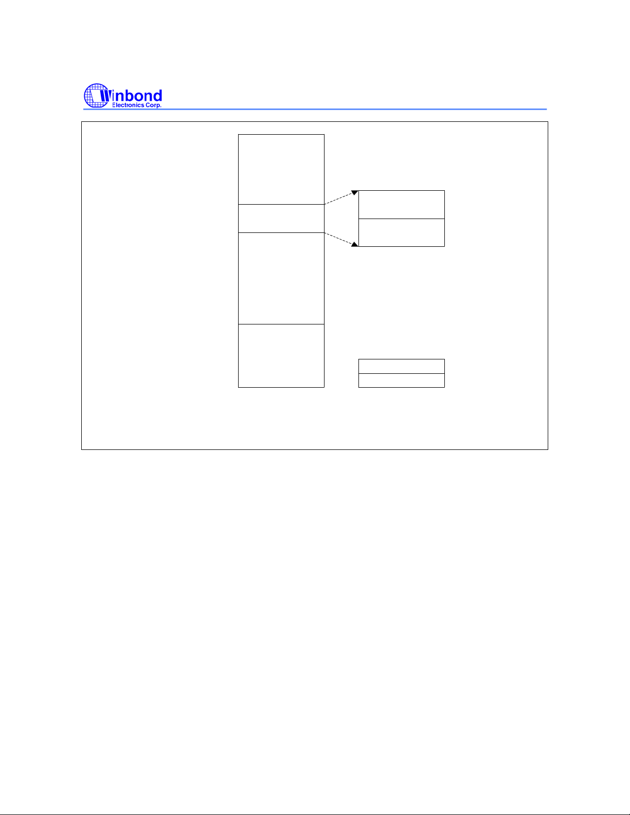
W79E825A/824A/823B/822B Data Sheet
FFFFH
Unused
Code Memory
FC7FH
FC00H
1000H/0800H
0FFFH/07FFH
0000H
On-Chip Code Memory Space
128 Bytes
NVM
Data Mem o ry
Unused
Code Memory
4K/2K Bytes
On-Chip
Code Memory
Figure 7-2: W79E823/822 Memory Map
NVM Data Memory area
CONFIG 2
CONFIG 1
Page 1
64 bytes
Page 0
64 bytes
FC7FH
FC40H
FC3FH
FC00H
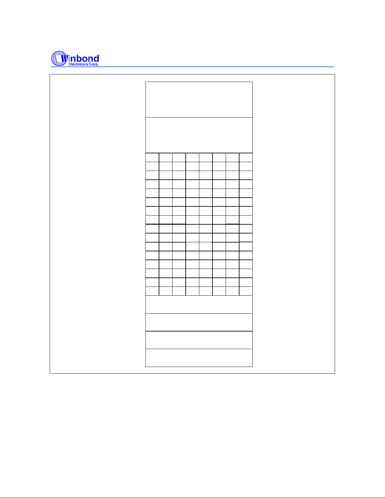
7.3 Register Map
As mentioned before the W79E825 series have separate Program and Data Memory areas. The onchip 256/128 bytes scratch pad RAM is in addition to the external memory. There are also several
Special Function Registers (SFRs) which can be accessed by software. The SFRs can be accessed
only by direct addressing, while the on-chip RAM can be accessed by either direct or indirect
addressing.
Publication Release Date: May 3, 2007
- 13 - Revision A7.1

W79E825A/824A/823B/822B Data Sheet
FFH
Indirect
RAM
Addressing
80H
7FH
00H
Figure 7-3: W79E825 and W79E824 RAM and SFR memory map
Direct
&
Indirect
RAM
Addressing
RAM and SFR Data Memory Space
SFR
Direct
Addressing
Only
FFH
Unused
Indirect
RAM
SFR
Direct
Addressing
Only
80H
7FH
Direct & Indirect
RAM
Addressing
00H
RAM and SFR Data Memory Space
Figure 7-4: W79E823 and W79E822 RAM and SFR memory map
Since the scratch-pad RAM is only 256/128 bytes it can be used only when data contents are small.
There are several other special purpose areas within the scratch-pad RAM. These are described as
follows.
- 14 -
W79E825A/824A/823B/822B Data Sheet
FFH
Indirect RAM
80H
7FH
Direct RAM
30H
34
Bank 3
Bank 2
Bank 1
Bank 0
7B 7A 79 787C7D7E7F
73 72 71 7074757677
6B 6A 69 686C6D6E6F
63 62 61 6064656667
5B 5A 59 585C5D5E5F
53 52 51 5054555657
4B 4A 49 484C4D4E4F
43 42
3B 3A 39 383C3D3E3F
33
32
2B 2A 29 282C2D2E2F
23 22 21 2024252627
1B 1A 19 181C1D1E1F
13 12 11 1014151617
0B 0A 09 080C0D0E0F
03 02 01 0004050607
41
31
4044
30
2FH
2EH
2DH
2CH
2BH
2AH
29H
28H
27H
26H
25H
24H
23H
22H
21H
20H
1FH
18H
17H
10H
0FH
08H
07H
00H
454647
353637
Figure 7-5: Scratch pad RAM
- 15 - Revision A7.1
Publication Release Date: May 3, 2007

W79E825A/824A/823B/822B Data Sheet
7.4 Working Registers
There are four sets of working registers, each consisting of eight 8-bit registers. These are termed as
Banks 0, 1, 2, and 3. Individual registers within these banks can be directly accessed by separate
instructions. These individual registers are named as R0, R1, R2, R3, R4, R5, R6 and R7. However, at
one time the W79E825 series can work with only one particular bank. The bank selection is done by
setting RS1-RS0 bits in the PSW. The R0 and R1 registers are used to store the address for indirect
accessing.
7.5 Bit addressable Locations
The Scratch-pad RAM area from location 20h to 2Fh is byte as well as bit addressable. This means
that a bit in this area can be individually addressed. In addition some of the SFRs are also bit
addressable. The instruction decoder is able to distinguish a bit access from a byte access by the type
of the instruction itself. In the SFR area, any existing SFR whose address ends in a 0 or 8 is bit
addressable.
7.6 Stack
The scratch-pad RAM can be used for the stack. This area is selected by the Stack Pointer (SP),
which stores the address of the top of the stack. Whenever a jump, call or interrupt is invoked the
return address is placed on the stack. There is no restriction as to where the stack can begin in the
RAM. By default however, the Stack Pointer contains 07h at reset. The user can then change this to
any value desired. The SP will point to the last used value. Therefore, the SP will be incremented and
then address saved onto the stack. Conversely, while popping from the stack the contents will be read
first, and then the SP is decreased.
- 16 -
W79E825A/824A/823B/822B Data Sheet
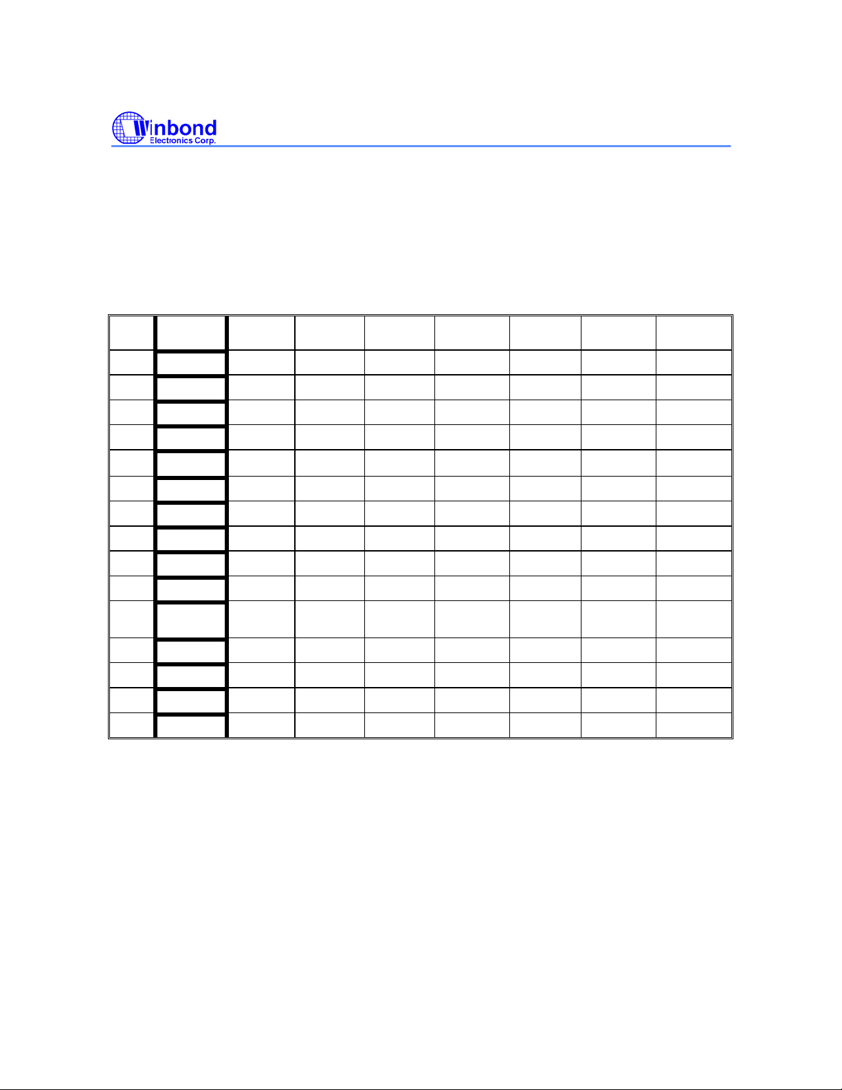
8. SPECIAL FUNCTION REGISTERS
The W79E825 series uses Special Function Registers (SFRs) to control and monitor peripherals and
their Modes. The SFRs reside in the register locations 80-FFh and are accessed by direct addressing
only. Some of the SFRs are bit addressable. This is very useful in cases where users wish to modify a
particular bit without changing the others. The SFRs that are bit addressable are those whose
addresses end in 0 or 8. The W79E825 series contain all the SFRs present in the standard 8052.
However some additional SFRs are added. In some cases the unused bits in the original 8052, have
been given new functions. The list of the SFRs is as follows.
F8
F0
E8
E0
D8
D0
C8
C0
B8
B0
A8
A0
98
90
88
80
IP1
B P0ID IP1H
EIE
ACC ADCCON ADCH
WDCON PWMPL PWM0L PWM1L PWMCON1 PWM2L
PSW PWMPH PWM0H PWM1H
NVMCON NVMDAT
I2CON I2ADDR NVMADDR TA
IP0 SADEN I2DAT I2STATUS I2CLK I2TIMER
P0M1 P0M2 P1M1 P1M2 P2M1 P2M2 IP0H
IE SADDR CMP1 CMP2
P2 KBI AUXR1
SCON SBUF
P1 DIVM
TCON TMOD TL0 TL1 TH0 TH1 CKCON
P0 SP DPL DPH PCON
PWM2H PWM3H PWMCON3
PWM3L PWMCON2
Table 8-1: Special Function Register Location Table
Note: 1. The SFRs in the column with dark borders are bit-addressable
2. The table is condensed with eight locations per row. Empty locations indicate that these are no registers at these
addresses. When a bit or register is not implemented, it will read high.
Publication Release Date: May 3, 2007
- 17 - Revision A7.1

W79E825A/824A/823B/822B Data Sheet
A
6
ADDR
SYMBOL DEFINITION
IP1 Interrupt priority 1 F8H
IP1H Interrupt high priority 1 F7H - - PPWMH PWDIH PC2H PC1H PKBH PI2H xx000000B
P0IDS
B B register F0H (F7) (F6) (F5) (F4) (F3) (F2) (F1) (F0) 00000000B
EIE Interrupt enable 1 E8H
ADCH ADC converter result E2H ADC.9 ADC.8 ADC.7 ADC.6 ADC.5 ADC.4 ADC.3 ADC.2 xxxxxxxxB
ADCCON ADC control register E1H ADC.1 ADC.0 ADCEX ADCI ADCS RCCLK AADR1 AADR0 xx000x00B
ACC Accumulator E0H (E7) (E6) (E5) (E4) (E3) (E2) (E1) (E0) 00000000B
PWMCON2 PWM control register 2 DFH BKCH BKPS BPEN BKEN PWM3B PWM2B PWM1B PWM0B 00000000B
PWM3L PWM 3 low bits register DEH PWM3.7 PWM3.6 PWM3.5 PWM3.4 PWM3.3 PWM3.2 PWM3.1 PWM3.0 00000000B
PWM2L PWM 2 low bits register DDH PWM2.7 PWM2.6 PWM2.5 PWM2.4 PWM2.3 PWM2.2 PWM2.1 PWM2.0 00000000B
PWMCON1 PWM control register 1 DCH PWMRUN load CF
PWM1L PWM 1 low bits register DBH PWM1.7 PWM1.6 PWM1.5 PWM1.4 PWM1.3 PWM1.2 PWM1.1 PWM1.0 00000000B
PWM0L PWM 0 low bits register DAH PWM0.7 PWM0.6 PWM0.5 PWM0.4 PWM0.3 PWM0.2 PWM0.1 PWM0.0 00000000B
PWMPL
WDCON Watch-Dog control D8H
PWMCON3 PWM control register 3 D7H - - - - - - - BKF xxxxxxx0B
PWM3H PWM 3 high bits register D6H - - - - - - PWM3.9 PWM3.8 xxxxxx00B
PWM2H PWM 2 high bits register D5H - - - - - - PWM2.9 PWM2.8 xxxxxx00B
PWM1H PWM 1 high bits register D3H - - - - - - PWM1.9 PWM1.8 xxxxxx00B
PWM0H PWM 0 high bits register D2H - - - - - - PWM0.9 PWM0.8 xxxxxx00B
PWMPH
PSW Program status word D0H
NVMDATA NVM Data CFH 00000000B
NVMCON NVM Control CEH EER EWR - - - - - - 00000000B
TA
NVMADDR NVM address C6H 00000000B
I2ADDR I2C address1 C1H ADDR.7 ADDR.6 ADDR.5 ADDR.4 ADDR.3 ADDR.2 ADDR.1 GC xxxxxxx0B
I2CON I2C Control register C0H
I2TIMER
I2CLK I2C Clock Rate BEH I2CLK.7 I2CLK.6 I2CLK.5 I2CLK.4 I2CLK.3 I2CLK.2 I2CLK.1 I2CLK.0 00000000B
I2STATUS BDH 00000000B
I2DAT BCH I2DAT.7 I2DAT.6 I2DAT.5 I2DAT.4 I2DAT.3 I2DAT.2 I2DAT.1 I2DAT.0 xxxxxxxxB
SADEN Slave address mask B9H 00000000B
IP0 Interrupt priority B8H
IP0H Interrupt high priority B7H - PADCH PBOH PSH PT1H PX1H PT0H PX0H x0000000B
P2M2 Port 2 output mode 2 B6H - - - - - - P2M2.1 P2M2.0 xxxxxx00B
P2M1 Port 2 output mode 1 B5H P2S P1S P0S ENCLK T1OE T0OE P2M1.1 P2M1.0 00000000B
P1M2 Port 1 output mode 2 B4H P1M2.7 P1M2.6 - P1M2.4 - - P1M2.1 P1M2.0 00000000B
P1M1 Port 1 output mode 1 B3H P1M1.7 P1M1.6 - P1M1.4 - - P1M1.1 P1M1.0 00000000B
P0M2 Port 0 output mode 2 B2H P0M2.7 P0M2.6 P0M2.5 P0M2.4 P0M2.3 P0M2.2 P0M2.1 P0M2.0 00000000B
P0M1 Port 0 output mode 1 B1H P0M1.7 P0M1.6 P0M1.5 P0M1.4 P0M1.3 P0M1.2 P0M1.1 P0M1.0 00000000B
Port 0 Digital Input
Disable
PWM counter low
register
PWM counter high
register
Timed Access
Protection
I2C Timer Counter
register
MSB BIT_
LSB
ESS
(FF) - (FE) - (FD)
F6H 00000000B
(EF) - (EE) - (ED)
D9H PWMP0.7 PWMP0.
(DF)
WDRUN
D1H - - - - - -
(D7)
CY
C7H TA.7 TA.6 TA.5 TA.4 TA.3 TA.2 TA.1 TA.0 00000000B
(CF) - (CE)
BFH - - - - - ENTI DIV4 TIF 00000000B
(BF) - (BE)
(DE) - (DD)
(D6)
AC
ENS1
PADC
PPWM
EPWM
PWMP0.5WMP0.4 PWMP0.3PWMP0.2PWMP0.1 PWMP0.000000000B
WD1
(D5)
F0
(CD)
STA
(BD)
PBO
(FC)
PWDI
(EC)
EWDI
(DC)
WD0
(D4)
RS1
(CC)
STO
(BC)
PS
DDRESS, SYMBOL
(FB)
PC2
(EB)
EC2
LRPWM PWM3I PWM2I PWM1I PWM0I 00000000B
(DB)
WDIF
(D3)
RS0
(CB)
SI
(BB)
PT1
(FA)
PC1
(EA)
EC1
(DA)
WTRF
(D2)
OV
(CA)
AA
(BA)
PX1
(F9)
PKB
(E9)
EKB
(D9)
EWRST
PWMP0.9 PWMP0.
(D1)
F1
(C9) - (C8)
(B9)
PT0
(F8)
PI2
(E8)
EI2
(D8)
WDCLR
8
(D0)
P
-
(B8)
PX0
RESET
xx000000B
xx000000B
0x000000B
xxxxxx00B
00000000B
x00000xxB
x0000000B
- 18 -

W79E825A/824A/823B/822B Data Sheet
A
Continued
ADDR
SYMBOL DEFINITION
CMP2
CMP1
SADDR Slave address A9H 00000000B
IE Interrupt enable A8H
AUXR1 AUX function register A2H KBF BOD BOI LPBOV SRST ADCEN 0 DPS 000X0000B
KBI Keyboard Interrupt A1H 00000000B
P2 Port 2 A0H
SBUF Serial buffer 99H xxxxxxxxB
SCON Serial control 98H
DIVM uC clock divide register 95H 00000000B
P1 Port 1 90H
CKCON Clock control 8EH - - - T1M T0M - - - xxx00xxxB
TH1 Timer high 1 8DH 00000000B
TH0 Timer high 0 8CH 00000000B
TL1 Timer low 1 8BH 00000000B
TL0 Timer low 0 8AH 00000000B
TMOD Timer mode 89H GATE C/T M1 M0 GATE C/T M1 M0 00000000B
TCON Timer control 88H
PCON Power control 87H SMOD SMOD0 BOF POR GF1 GF0 PD IDL 00xx0000B
DPH Data pointer high 83H 00000000B
DPL Data pointer low 82H 00000000B
SP Stack pointer 81H 00000111B
P0 Port 0 80H
Comparator 2 control
register
Comparator 1 control
register
MSB BIT_
ESS
LSB
ADH - - CE2 CP2 CN2 OE2 CO2 CMF2 00000000B
ACH - - CE1 CP1 CN1 OE1 CO1 CMF1 00000000B
(AF)
EA
(A7) - (A6) - (A5) - (A4) - (A3) - (A2) - (A1)
(9F)
SM0/FE
(97)
PWM2
(8F)
TF1
(87)
T1
(AE)
EADC
(9E)
SM1
(96)
PWM1
(8E)
TR1
(86)
AD3
CMP1
(AD)
EBO
(9D)
SM2
(95)
/RST
(8D)
TF0
(85)
AD2
CMPREF
(AC)
ES
(9C)
REN
(94)
/INT1
(8C)
TR0
(84)
AD1
CIN1A
Table 8-2: Special Function Registers
DDRESS, SYMBOL
(AB)
ET1
(9B)
TB8
(93)
/INT0
SDL
(8B)
IE1
(83)
AD0
CIN1B
(AA)
EX1
(9A)
RB8
(92)
T0
SCL
(8A)
IT1
(82)
BRAKE
CIN2A
(A9)
ET0
XTAL1
(99)
TI
(91)
RXD
(89)
IE0
(81)
PWM0
CIN2B
(A8)
EX0
(A0)
XTAL2
CLKOUT
(98)
RI
(90)
TXD
(88)
IT0
(80)
PWM3
CMP2
RESET
00000000B
xxxxxx11B
00000000B
11111111B
00000000B
11111111B
Publication Release Date: May 3, 2007
- 19 - Revision A7.1
W79E825A/824A/823B/822B Data Sheet
PORT 0
Bit: 7 6 5 4 3 2 1 0
P0.7 P0.6 P0.5 P0.4 P0.3 P0.2 P0.1 P0.0
Mnemonic: P0 Address: 80h
P0.7-0: General purpose Input/Output port. Most instructions will read the port pins in case of a port
read access, however in case of read-modify-write instructions, the port latch is read. These alternate
functions are described below:
BIT NAME FUNCTION
7 P0.7 Timer 1 pin or KBI.7 pin of keypad input.
6 P0.6 CMP1 pin of analog comparator or KBI.6 pin of keypad input or AD3 of AD converter.
5 P0.5 CMPREF pin of analog comparator or KBI.5 pin of keypad input or AD2 of AD
converter.
4 P0.4 CIN1A pin of analog comparator or KBI.4 pin of keypad input or AD1 of AD converter
3 P0.3 CIN1B pin of analog comparator or KBI.3 pin of keypad input or AD0 of AD converter.
2 P0.2 BRAKE pin of PWM or CIN2A pin of analog comparator or KBI.2 pin of keypad input.
1 P0.1 PWM0 pin or CIN2B pin of analog comparator or KBI.1 pin of keypad input.
0 P0.0 PWM3 pin or CMP2 pin of analog comparator or KBI.0 pin of keypad input.
Note: The initial value of the port is set by CONFIG1.PRHI bit. The default setting for CONFIG1.PRHI =1 which the alternative
function output is turned on upon reset. If CONFIG1.PRHI is set to 0, the user has to write a 1 to port SFR to turn on the
alternative function output.
STACK POINTER
Bit: 7 6 5 4 3 2 1 0
SP.7 SP.6 SP.5 SP.4 SP.3 SP.2 SP.1 SP.0
Mnemonic: SP Address: 81h
BIT NAME FUNCTION
7-0 SP.[7:0]
DATA POINTER LOW
Bit: 7 6 5 4 3 2 1 0
DPL.7 DPL.6 DPL.5 DPL.4 DPL.3 DPL.2 DPL.1 DPL.0
Mnemonic: DPL Address: 82h
BIT NAME FUNCTION
7-0 DPL.[7:0] This is the low byte of the standard 8052 16-bit data pointer.
The Stack Pointer stores the Scratch-pad RAM address where the stack begins. In
other words it always points to the top of the stack.
DATA POINTER HIGH
Bit: 7 6 5 4 3 2 1 0
DPH.7 DPH.6 DPH.5 DPH.4 DPH.3 DPH.2 DPH.1 DPH.0
Mnemonic: DPH Address: 83h
- 20 -
W79E825A/824A/823B/822B Data Sheet
BIT NAME FUNCTION
7-0 DPH.[7:0]
POWER CONTROL
Bit: 7 6 5 4 3 2 1 0
SMOD SMOD0 BOF POR GF1 GF0 PD IDL
Mnemonic: PCON Address: 87h
BIT NAME FUNCTION
7 SMOD 1: This bit doubles the serial port baud rate in mode 1, 2, and 3.
6 SMOD0
5 BOF
This is the high byte of the standard 8052 16-bit data pointer.
This is the high byte of the DPTR 16-bit data pointer.
0: Framing Error Detection Disable. SCON.7 (SM0/FE) bit is used as SM0
(standard 8052 function).
1: Framing Error Detection Enable. SCON.7 (SM0/FE) bit is used to reflect as
Frame Error (FE) status flag.
0: Cleared by software.
1: Set automatically when a brownout reset or interrupt has occurred. Also set at
power on.
4 POR
3 GF1 General purpose user flags.
2 GF0 General purpose user flags.
1 PD
0 IDL
TIMER CONTROL
Bit: 7 6 5 4 3 2 1 0
TF1 TR1 TF0 TR0 IE1 IT1 IE0 IT0
Mnemonic: TCON Address: 88h
BIT NAME FUNCTION
7 TF1
6 TR1
0: Cleared by software.
1: Set automatically when a power-on reset has occurred.
1: The CPU goes into the POWER DOWN mode. In this mode, all the clocks are
stopped and program execution is frozen.
1: The CPU goes into the IDLE mode. In this mode, the clocks CPU clock
stopped, so program execution is frozen. But the clock to the serial, timer and
interrupt blocks is not stopped, and these blocks continue operating.
Timer 1 Overflow Flag. This bit is set when Timer 1 overflows. It is cleared
automatically when the program does a timer 1 interrupt service routine. Software
can also set or clear this bit.
Timer 1 Run Control. This bit is set or cleared by software to turn timer/counter on
or off.
Publication Release Date: May 3, 2007
- 21 - Revision A7.1

W79E825A/824A/823B/822B Data Sheet
Continued
BIT NAME FUNCTION
Timer 0 Overflow Flag. This bit is set when Timer 0 overflows. It is cleared
5 TF0
automatically when the program does a timer 0 interrupt service routine. Software
can also set or clear this bit.
4 TR0
3 IE1
2 IT1
1 IE0
0 IT0
TIMER MODE CONTROL
Bit: 7 6 5 4 3 2 1 0
GATE
TIMER1 TIMER0
Mnemonic: TMOD Address: 89h
BIT NAME FUNCTION
Timer 0 Run Control. This bit is set or cleared by software to turn timer/counter on
or off.
Interrupt 1 Edge Detect Flag: Set by hardware when an edge/level is detected on
INT1
. This bit is cleared by hardware when the service routine is vectored to only if
the interrupt was edge triggered. Otherwise it follows the inverse of the pin.
Interrupt 1 Type Control. Set/cleared by software to specify falling edge/ low level
triggered external inputs.
Interrupt 0 Edge Detect Flag. Set by hardware when an edge/level is detected on
INT0
. This bit is cleared by hardware when the service routine is vectored to only if
the interrupt was edge triggered. Otherwise it follows the inverse of the pin.
Interrupt 0 Type Control: Set/cleared by software to specify falling edge/ low level
triggered external inputs.
TC /
M1 M0 GATE
TC /
M1 M0
Gating control: When this bit is set, Timer/counter 1 is enabled only while the
GATE
7
6
M1 Timer 1 mode select bit 1. See table below.
5
M0 Timer 1 mode select bit 0. See table below.
4
GATE
3
2
M1 Timer 0 mode select bit 1. See table below.
1
M0 Timer 0 mode select bit 0. See table below.
0
pin is high and the TR1 control bit is set. When cleared, the
and Timer 1 is enabled whenever TR1 control bit is set.
Timer or Counter Select: When clear, Timer 1 is incremented by the internal clock.
TC/
When set, the timer counts falling edges on the T1 pin.
Gating control: When this bit is set, Timer/counter 0 is enabled only while the
pin is high and the TR0 control bit is set. When cleared, the
and Timer 0 is enabled whenever TR0 control bit is set.
Timer or Counter Select: When clear, Timer 0 is incremented by the internal clock.
TC/
When set, the timer counts falling edges on the T0 pin.
INT1
INT1 pin has no effect,
INT0
INT0 pin has no effect,
- 22 -
W79E825A/824A/823B/822B Data Sheet
M1, M0: Mode Select bits:
M1 M0 MODE
0 0
Mode 0: 8-bit timer/counter TLx serves as 5-bit pre-scale.
0 1
1 0
1 1
TIMER 0 LSB
Bit: 7 6 5 4 3 2 1 0
TL0.7 TL0.6 TL0.5 TL0.4 TL0.3 TL0.2 TL0.1 TL0.0
Mnemonic: TL0 Address: 8Ah
BIT NAME FUNCTION
7-0 TL0.[7:0] Timer 0 LSB.
TIMER 1 LSB
Bit: 7 6 5 4 3 2 1 0
TL1.7 TL1.6 TL1.5 TL1.4 TL1.3 TL1.2 TL1.1 TL1.0
Mnemonic: TL1 Address: 8Bh
BIT NAME FUNCTION
7-0 TL1.[7:0] Timer 1 LSB.
Mode 1: 16-bit timer/counter, no pre-scale.
Mode 2: 8-bit timer/counter with auto-reload from THx.
Mode 3: (Timer 0) TL0 is an 8-bit timer/counter controlled by the standard Timer0
control bits. TH0 is an 8-bit timer only controlled by Timer1 control bits.
(Timer 1) Timer/Counter 1 is stopped.
TIMER 0 MSB
Bit: 7 6 5 4 3 2 1 0
TH0.7 TH0.6 TH0.5 TH0.4 TH0.3 TH0.2 TH0.1 TH0.0
Mnemonic: TH0 Address: 8Ch
BIT NAME FUNCTION
7-0 TH0.[7:0] Timer 0 MSB.
TIMER 1 MSB
Bit: 7 6 5 4 3 2 1 0
TH1.7 TH1.6 TH1.5 TH1.4 TH1.3 TH1.2 TH1.1 TH1.0
Mnemonic: TH1 Address: 8Dh
BIT NAME FUNCTION
7-0 TH1.[7:0] Timer 1 MSB.
Publication Release Date: May 3, 2007
- 23 - Revision A7.1
W79E825A/824A/823B/822B Data Sheet
CLOCK CONTROL
Bit: 7 6 5 4 3 2 1 0
- - - T1M T0M - - -
Mnemonic: CKCON Address: 8Eh
BIT NAME FUNCTION
7-5
4
3
- Reserved.
Timer 1 clock select:
T1M
T0M
0: Timer 1 uses a divide by 12 clocks.
1: Timer 1 uses a divide by 4 clocks.
Timer 0 clock select:
0: Timer 0 uses a divide by 12 clocks.
1: Timer 0 uses a divide by 4 clocks.
2-0
PORT 1
Bit: 7 6 5 4 3 2 1 0
P1.7 P1.6 P1.5 P1.4 P1.3 P1.2 P1.1 P1.0
Mnemonic: P1 Address: 90h
P1.7-0: General purpose Input/Output port. Most instructions will read the port pins in case of a port
read access, however in case of read-modify-write instructions, the port latch is read. These alternate
functions are described below:
BIT NAME FUNCTION
7 P1.7 PWM 2 Pin.
6 P1.6 PWM 1 Pin.
5 P1.5 /RST Pin or Input Pin by alternative.
4 P1.4 /INT1 interrupt.
3 P1.3 /INT0 interrupt or SDA of I2C.
2 P1.2 Timer 0 or SCL of I2C.
1 P1.1 RXD of Serial port.
0 P1.0 TXD of Serial port.
Note: The initial value of the port is set by CONFIG1.PRHI bit. The default setting for CONFIG1.PRHI =1 which the alternative
function output is turned on upon reset. If CONFIG1.PRHI is set to 0, the user has to write a 1 to port SFR to turn on the
alternative function output.
- Reserved.
DIVIDER CLOCK
Bit: 7 6 5 4 3 2 1 0
DIVM.7 DIVM.6 DIVM.5 DIVM.4 DIVM.3 DIVM.2 DIVM.1 DIVM.0
Mnemonic: DIVM Address: 95h
- 24 -
W79E825A/824A/823B/822B Data Sheet
BIT NAME FUNCTION
7-0 DIVM.[7:0] The DIVM register is clock divider of uC. Refer OSCILLATOR chapter.
SERIAL PORT CONTROL
Bit: 7 6 5 4 3 2 1 0
SM0/FE SM1 SM2 REN TB8 RB8 TI RI
Mnemonic: SCON Address: 98h
BIT NAME FUNCTION
Serial port mode select bit 0 or Framing Error Flag: The SMOD0 bit in PCON SFR
SM0/FE
7
SM1 Serial Port mode select bit 1. See table below.
6
SM2
5
determines whether this bit acts as SM0 or as FE. The operation of SM0 is
described below. When used as FE, this bit will be set to indicate an invalid stop
bit. This bit must be manually cleared in software to clear the FE condition.
Multiple processors communication. Setting this bit to 1 enables the multiprocessor
communication feature in mode 2 and 3. In mode 2 or 3, if SM2 is set to 1, then RI
will not be activated if the received 9th data bit (RB8) is 0. In mode 1, if SM2 = 1,
then RI will not be activated if a valid stop bit was not received. In mode 0, the SM2
bit controls the serial port clock. If set to 0, then the serial port runs at a divide by
12 clock of the oscillator. This gives compatibility with the standard 8052. When set
to 1, the serial clock become divide by 4 of the oscillator clock. This results in faster
synchronous serial communication.
4
3
2
1
0
REN
TB8
RB8
TI
RI
Receive enable:
0: Disable serial reception.
1: Enable serial reception.
This is the 9th bit to be transmitted in modes 2 and 3. This bit is set and cleared by
software as desired.
In modes 2 and 3 this is the received 9th data bit. In mode 1, if SM2 = 0, RB8 is the
stop bit that was received. In mode 0 it has no function.
Transmit interrupt flag: This flag is set by hardware at the end of the 8th bit time in
mode 0, or at the beginning of the stop bit in all other modes during serial
transmission. This bit must be cleared by software.
Receive interrupt flag: This flag is set by hardware at the end of the 8th bit time in
mode 0, or halfway through the stop bits time in the other modes during serial
reception. However the restrictions of SM2 apply to this bit. This bit can be cleared
only by software.
Publication Release Date: May 3, 2007
- 25 - Revision A7.1

W79E825A/824A/823B/822B Data Sheet
SM1, SM0: Mode Select bits:
MODE SM1 SM0 DESCRIPTION LENGTH BAUD RATE
0 0 0 Synchronous 8
1 0 1 Asynchronous 10
2 1 0 Asynchronous 11
3 1 1 Asynchronous 11
SERIAL DATA BUFFER
Bit: 7 6 5 4 3 2 1 0
SBUF.7 SBUF.6 SBUF.5 SBUF.4 SBUF.3 SBUF.2 SBUF.1 SBUF.0
Mnemonic: SBUF Address: 99h
BIT NAME FUNCTION
Serial data on the serial port is read from or written to this location. It actually
7-0 SBUF.[7:0]
consists of two separate internal 8-bit registers. One is the receive resister, and
the other is the transmit buffer. Any read access gets data from the receive data
buffer, while write access is to the transmit data buffer.
Tclk divided by 4 or 12
Variable
Tclk divided by 32 or 64
Variable
PORT 2
Bit: 7 6 5 4 3 2 1 0
- - - - - - P2.1 P2.0
Mnemonic: P2 Address: A0h
BIT NAME FUNCTION
7-2 - Reserved
1 P2.1 XTAL1 clock input pin.
0 P2.0 XTAL2 or CLKOUT pin by alternative.
Note: The initial value of the port is set by CONFIG1.PRHI bit. The default setting for CONFIG1.PRHI =1 which the alternative
function output is turned on upon reset. If CONFIG1.PRHI is set to 0, the user has to write a 1 to port SFR to turn on the
alternative function output.
KEYBOARD INTERRUPT
Bit: 7 6 5 4 3 2 1 0
KBI.7 KBI.6 KBI.5 KBI.4 KBI.3 KBI.2 KBI.1 KBI.0
Mnemonic: KBI Address: A1h
BIT NAME FUNCTION
7
6
KBI.7 1: Enable P0.7 as a cause of a Keyboard interrupt.
KBI.6 1: Enable P0.6 as a cause of a Keyboard interrupt.
5
4
KBI.5 1: Enable P0.5 as a cause of a Keyboard interrupt.
KBI.4 1: Enable P0.4 as a cause of a Keyboard interrupt.
- 26 -
W79E825A/824A/823B/822B Data Sheet
Continued .
BIT NAME FUNCTION
3
KBI.3 1: Enable P0.3 as a cause of a Keyboard interrupt.
2
1
0
AUX FUNCTION REGISTER 1
Bit: 7 6 5 4 3 2 1 0
KBF BOD BOI LPBOV SRST ADCEN 0 DPS
Mnemonic: AUXR1 Address: A2h
BIT NAME FUNCTION
7 KBF
6 BOD
5 BOI
KBI.2 1: Enable P0.2 as a cause of a Keyboard interrupt.
KBI.1 1: Enable P0.1 as a cause of a Keyboard interrupt.
KBI.0 1: Enable P0.0 as a cause of a Keyboard interrupt.
Keyboard Interrupt Flag:
1: When any pin of port 0 that is enabled for the Keyboard Interrupt function goes
low. Must be cleared by software.
Brown Out Disable:
0: Enable Brownout Detect function.
1: Disable Brownout Detect function and save power.
Brown Out Interrupt:
0: Disable Brownout Detect Interrupt function and it will cause chip reset when
BOF is set.
1: This prevents Brownout Detection from causing a chip reset and allows the
Brownout Detect function to be used as an interrupt.
Low Power Brown Out Detect control:
0: When BOD is enable, the Brown Out detect is always turned on by normal run
or Power Down mode.
4 LPBOV
3 SRST
2 ADCEN
1 0 Reserved.
0 DPS
1: When BOD is enable, the Brown Out detect circuit is turned on by Power
Down mode. This control can help save 15/16 of the Brownout circuit power.
When uC is in Power Down mode, the BOD will enable internal RC OSC
(2MHz~0.5MHZ)
Software reset:
1: reset the chip as if a hardware reset occurred.
0: Disable ADC circuit.
1: Enable ADC circuit.
Dual Data Pointer Select
0: To select DPTR of standard 8051.
1: To select DPTR1
Publication Release Date: May 3, 2007
- 27 - Revision A7.1
W79E825A/824A/823B/822B Data Sheet
INTERRUPT ENABLE
Bit: 7 6 5 4 3 2 1 0
EA EADC EBO ES ET1 EX1 ET0 EX0
Mnemonic: IE Address: A8h
BIT NAME FUNCTION
7 EA Global enable. Enable/Disable all interrupts.
6 EADC Enable ADC interrupt.
5 EBO Enable Brown Out interrupt.
4 ES Enable Serial Port interrupt.
3 ET1 Enable Timer 1 interrupt.
2 EX1 Enable external interrupt 1.
1 ET0 Enable Timer 0 interrupt.
0 EX0 Enable external interrupt 0.
SLAVE ADDRESS
Bit: 7 6 5 4 3 2 1 0
SADDR.7 SADDR.6 SADDR.5 SADDR.4 SADDR.3 SADDR.2 SADDR.1 SADDR.0
Mnemonic: SADDR Address: A9h
BIT NAME FUNCTION
7-0 SADDR.[7:0]
COMPARATOR 1 CONTROL REGISTER
Bit: 7 6 5 4 3 2 1 0
- - CE1 CP1 CN1 OE1 CO1 CMF1
Mnemonic: CMP1 Address: ACh
BIT NAME FUNCTION
7 - Reserved.
6 - Reserved.
5 CE1
4 CP1
The SADDR should be programmed to the given or broadcast address for
serial port to which the slave processor is designated.
Comparator enable:
0: Disable Comparator.
1: Enabled Comparator. Comparator output need wait stable 10 us after CE1 is
first set.
Comparator positive input select:
0: CIN1A is selected as the positive comparator input.
1: CIN1B is selected as the positive comparator input.
- 28 -

W79E825A/824A/823B/822B Data Sheet
Continued.
BIT NAME FUNCTION
Comparator negative input select:
0: The comparator reference pin CMPREF is selected as the negative
3 CN1
2 OE1
1 CO1
0 CMF1
comparator input.
1: The internal comparator reference Vref is selected as the negative comparator
input.
Output enable:
1: The comparator output is connected to the CMP1 pin if the comparator is
enabled (CE1 = 1). This output is asynchronous to the CPU clock.
Comparator output:
Synchronized to the CPU clock to allow reading by software. Cleared when the
comparator is disabled (CE1 = 0).
Comparator interrupt flag:
This bit is set by hardware whenever the comparator output CO1 changes state.
This bit will cause a hardware interrupt if enabled and of sufficient priority.
Cleared by software and when the comparator is disabled (CE1 = 0).
COMPARATOR 2 CONTROL REGISTER
Bit: 7 6 5 4 3 2 1 0
- - CE2 CP2 CN2 OE2 CO2 CMF2
Mnemonic: CMP2 Address: ADh
BIT NAME FUNCTION
7 - Reserved.
6 - Reserved.
Comparator enable:
5 CE2
4 CP2
3 CN2
0: Disable Comparator.
1: Enabled Comparator. Comparator output need wait stable 10 us after CE2 is
first set.
Comparator positive input select:
0: CIN2A is selected as the positive comparator input.
1: CIN2B is selected as the positive comparator input.
Comparator negative input select:
0: The comparator reference pin CMPREF is selected as the negative
comparator input.
1: The internal comparator reference Vref is selected as the negative comparator
input.
Publication Release Date: May 3, 2007
- 29 - Revision A7.1
W79E825A/824A/823B/822B Data Sheet
Continued .
BIT NAME FUNCTION
Output enable:
2 OE2
1 CO2
0 CMF2
PORT 0 OUTPUT MODE 1
Bit: 7 6 5 4 3 2 1 0
P0M1.7 P0M1.6 P0M1.5 P0M1.4 P0M1.3 P0M1.2 P0M1.1 P0M1.0
Mnemonic: P0M1 Address: B1h
1: The comparator output is connected to the CMP2 pin if the comparator is
enabled (CE2 = 1). This output is asynchronous to the CPU clock.
Comparator output:
Synchronized to the CPU clock to allow reading by software. Cleared when the
comparator is disabled (CE2 = 0).
Comparator interrupt flag:
This bit is set by hardware whenever the comparator output CO2 changes state.
This bit will cause a hardware interrupt if enabled and of sufficient priority.
Cleared by software and when the comparator is disabled (CE2 = 0).
BIT NAME FUNCTION
7-0 P0M1.[7:0] To control the output configuration of P0 bits [7:0]
PORT 0 OUTPUT MODE 2
Bit: 7 6 5 4 3 2 1 0
P0M2.7 P0M2.6 P0M2.5 P0M2.4 P0M2.3 P0M2.2 P0M2.1 P0M2.0
Mnemonic: P0M2 Address: B2h
BIT NAME FUNCTION
7-0 P0M2.[7:0] To control the output configuration of P0 bits [7:0]
PORT 1 OUTPUT MODE 1
Bit: 7 6 5 4 3 2 1 0
P1M1.7 P1M1.6 P1M1.5 P1M1.4 P1M1.3 P1M1.2 P1M1.1 P1M1.0
Mnemonic: P1M1 Address: B3h
BIT NAME FUNCTION
7-0 P1M1.[7:0] To control the output configuration of P1 bits [7:0]
PORT 1 OUTPUT MODE 2
Bit: 7 6 5 4 3 2 1 0
P1M2.7 P1M2.6 P1M2.5 P1M2.4 P1M2.3 P1M2.2 P1M2.1 P1M2.0
Mnemonic: P1M2 Address: B4h
- 30 -
 Loading...