

Winbond Electronics W78LE812P-24, W78LE812F-24, W78LE812-24 Datasheet

W78LE812
8-BIT MTP MICROCONTROLLER
GENERAL DESCRIPTION
The W78LE812 is an 8-bit microcontroller which can accommodate a wide range of supply voltages
with low power consumption. The instruction set for the W78LE812 is fully compatible with the
standard 8051. The W78LE812 contains an 8K bytes MTP ROM (Multiple-Time Programmable
ROM); a 256 bytes RAM; four 8-bit bi-directional and bit-addressable I/O ports; an additional 6-bit I/O
port P4; three 16-bit timer/counters; a hardware watchdog timer and a serial port. These peripherals
are supported by a fourteen sources two-level interrupt capability. To facilitate programming and
verification, the MTP-ROM inside the W78LE812 allows the program memory to be programmed and
read electronically. Once the code is confirmed, the user can protect the code for security.
The W78LE812 microcontroller has two power reduction modes, idle mode and power-down mode,
both of which are software selectable. The idle mode turns off the processor clock but allows for
continued peripheral operation. The power-down mode stops the crystal oscillator for minimum power
consumption. The external clock can be stopped at any time and in any state without affecting the
processor.
FEATURES
• Fully static design 8-bit CMOS microcontroller
• Wide supply voltage of 2.4V to 5.5V
• 256 bytes of on-chip scratchpad RAM
• 8 KB electrically erasable/programmable MTP-ROM
• 64 KB program memory address space
• 64 KB data memory address space
• Four 8-bit bi-directional ports
• Three 16-bit timer/counters
• Timer 2 Clock-out
• One full duplex serial port(UART)
• Watchdog Timer
• Direct LED drive outputs
• Fourteen sources, two-level interrupt capability
• Wake-up via external interrupts at Port 1
• EMI reduction mode
• Built-in power management
• Code protection mechanism
• Packages:
− DIP 40: W78LE812-24
− PLCC 44: W78LE812P-24
− PQFP 44: W78LE812F-24
Publication Release Date: February 1999
- 1 - Revision A2
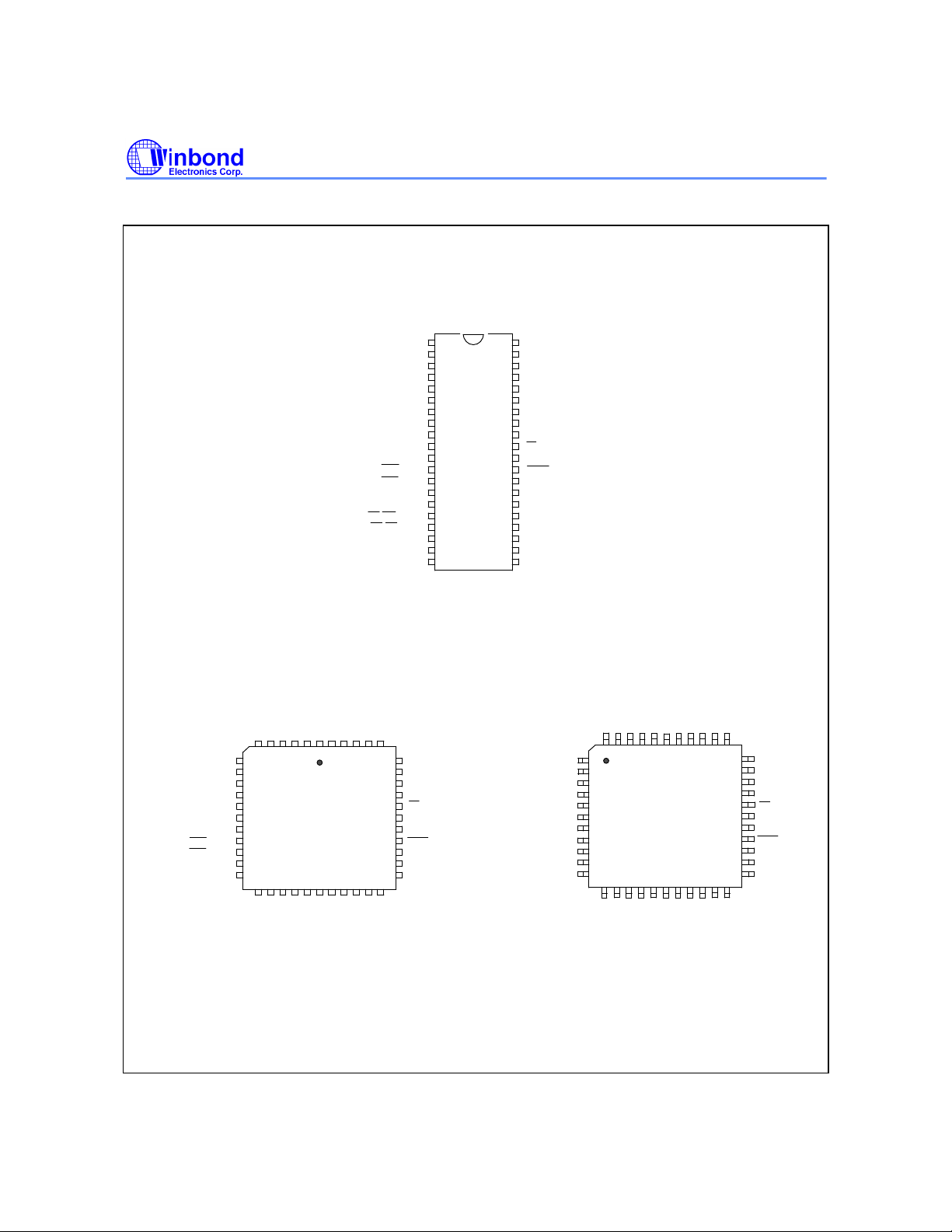
PIN CONFIGURATIONS
40-Pin DIP (W78LE812)
INT2,,T2, P1.0
INT3,T2EX, P1.1
INT4,P1.2
INT5,P1.3
INT6,P1.4
INT7,P1.5
INT8,P1.6
INT9,P1.7
A9CTRL,RXD, P3.0
A13CTR,LTXD, P3.1
A14CTRL,INT0, P3.2
OECTRL,INT1, P3.3
T0, P3.4
T1, P3.5
CE,WR, P3.6
OE,RD, P3.7
XTAL2
XTAL1
RST
VSS
W78LE812
VDD1
2
3
4
5
6
7
8
9
10
11
12
13
14
15
16
17
18
19
20
40
39
P0.0, AD0
38
P0.1, AD1
P0.2, AD2
37
P0.3, AD3
36
35
P0.4, AD4
34
P0.5, AD5
33
P0.6, AD6
32
P0.7, AD7
31
EA,VPP
30
ALE,P4.5
29
PSEN,P4.6
28
P2.7, A15
27
P2.6, A14
P2.5, A13
26
25
P2.4, A12
P2.3, A11
24
P2.2, A10
23
22
P2.1, A9
21
P2.0, A8
INT7,P1.5
INT8,P1.6
INT9,P1.7
A9CTRL,RXD, P3.0
A13CTRL,TXD, P3.1
A14CTRL,INT0, P3.2
OECTRL,INT1, P3.3
T0, P3.4
T1, P3.5
44-Pin PLCC (W78LE812P)
I
N
T
I
3
N
,
T
T
I
I
I
2
2
N
T
5
,
P
1
.
3
P
3
.
7
,
/
R
D
,
/
O
E
N
E
T
X
4
,
,
P
P
1
1
.
.
2
1
X
X
T
T
A
A
L
L
1
2
,
T
2
,
P
P
1
4
.
.
0
2
2 1 44 43 42
V
P
S
4
S
.
0
RST
P4.3
N
T
6
,
P
1
.
4
6 5 4 3
7
8
9
10
11
12
13
14
15
16
17
P
3
.
6
,
/
W
R
,
/
C
E
44-Pin PQFP (W78LE812F)
I
N
T
I
3
N
,
T
T
I
I
I
2
2
N
N
T
T
4
5
,
,
P
P
1
1
.
.
2
3
43 4241
X
P
T
3
A
.
L
7
2
,
/
R
D
,
/
O
E
,
T
E
2
X
,
,
P
P
P
1
1
4
.
.
.
0
1
2
40 39 38 37 36
X
V
P
T
S
4
A
S
.
L
0
1
V
D
D
P
2
.
0
,
A
8
RST
N
T
6
,
P
1
.
4
1
2
3
4
5
6
7
8
9
10
11
P
3
.
6
,
/
W
R
,
/
C
E
A
A
A
A
D
D
D
D
3
2
1
0
,
,
,
,
P
P
P
P
V
D
D
P
2
.
0
,
A
8
0
0
0
0
.
.
.
.
3
2
1
0
40
41
P0.4, AD4
39
38
P0.5, AD5
37
P0.6, AD6
36
P0.7, AD7
35
EA,VPP
34
P4.1
33
ALE,P4.5
32
PSEN,P4.6
31
P2.7, A15
30
P2.6, A14
29
P2.5, A13
2827262524232221201918
P
P
P
P
2
2
2
2
.
.
.
.
3
4
2
1
,
,
,
,
A
A
A
A
1
1
9
1
2
1
0
INT7,P1.5
INT8,P1.6
INT9,P1.7
A9CTRL,RXD, P3.0
A13CTRL,TXD, P3.1
A14CTRL,INT0, P3.2
OECTRL,INT1, P3.3
T0, P3.4
T1, P3.5
P4.3
A
A
A
A
D
D
D
D
3
2
1
0
,
,
,
,
P
P
P
P
0
0
0
0
.
.
.
.
3
1
2
0
34
3544
P
P
P
2
2
2
.
.
.
3
2
1
,
,
,
A
A
A
1
1
9
1
0
P0.4, AD4
33
32
P0.5, AD5
31
P0.6, AD6
30
P0.7, AD7
29
EA,VPP
28
P4.1
27
ALE,P4.5
26
PSEN,P4.6
25
P2.7, A15
24
P2.6, A14
23
P2.5, A13
2221201918171615141312
P
2
.
4
,
A
1
2
- 2 -
W78LE812
EA
INT
1
WR
RD
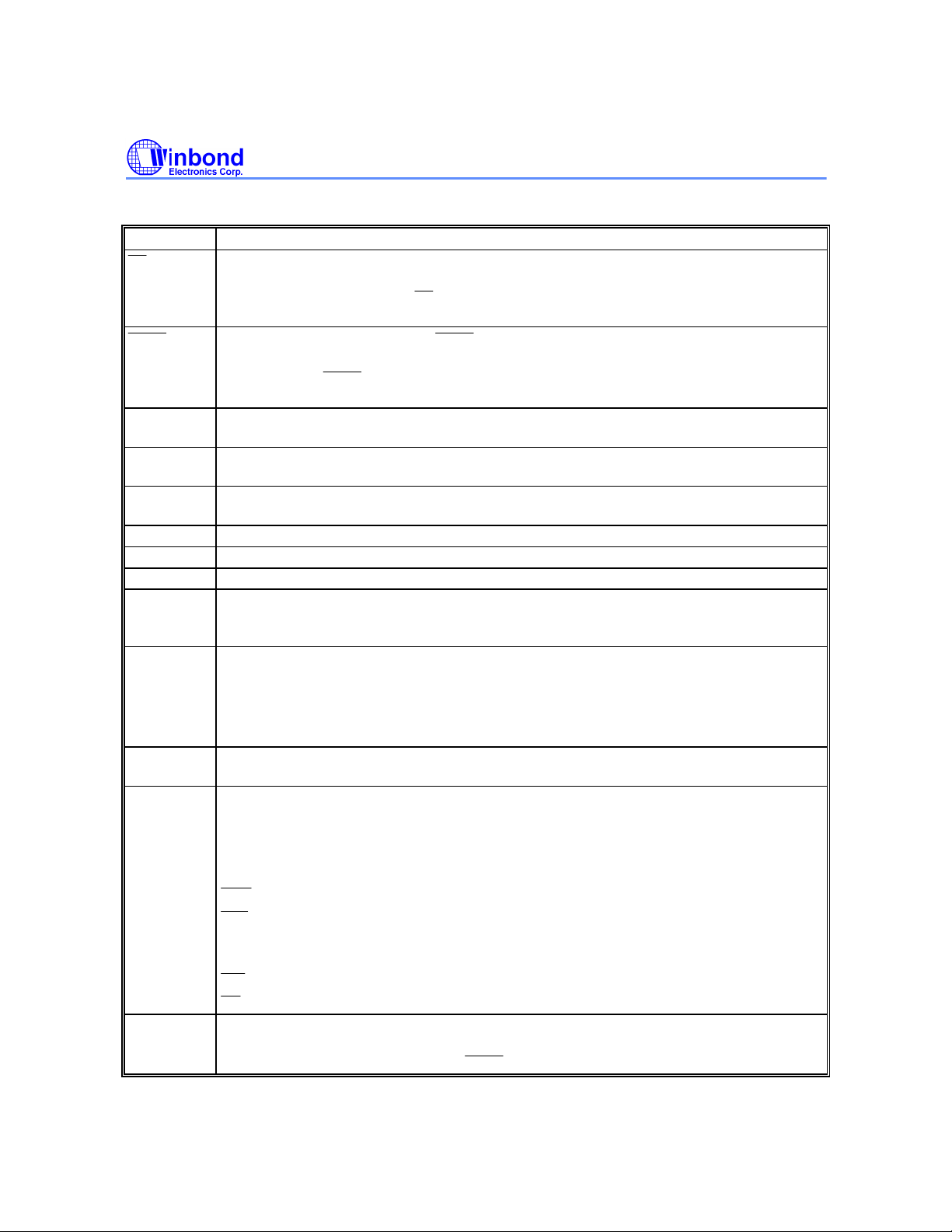
PIN DESCRIPTION
SYMBOL DESCRIPTIONS
EXTERNAL ACCESS ENABLE: This pin forces the processor to execute out of external
ROM. It should be kept high to access internal ROM. The ROM address and data will
not be present on the bus if EA pin is high and the program counter is within on-chip
ROM area. Otherwise they will be present on the bus.
PSEN
ALE ADDRESS LATCH ENABLE: ALE is used to enable the address latch that separates
RST RESET: A high on this pin for two machine cycles while the oscillator is running resets
XTAL1 CRYSTAL1: This is the crystal oscillator input. This pin may be driven by an external
XTAL2 CRYSTAL2: This is the crystal oscillator output. It is the inversion of XTAL1.
VSS GROUND: Ground potential
VDD POWER SUPPLY: Supply voltage for operation.
P0.0−P0.7
P1.0−P1.7
P2.0−P2.7
P3.0−P3.7
P4.0-P4.6 PORT 4: A 6-bit bi-directional I/O port which is bit-addressable. Pins P4.0 to P4.3 are
PROGRAM STORE ENABLE:
address/data bus during fetch and MOVC operations. When internal ROM access is
performed, no
alternative function P4.6.
the address from the data on Port 0. This pin also serves the alternative function P4.5
the device.
clock.
PORT 0: Port 0 is a bi-directional I/O port which also provides a multiplexed low order
address/data bus during accesses to external memory. The pins of Port 0 can be
individually configured to open-drain or standard port with internal pull-ups.
PORT 1: Port 1 is a bi-directional I/O port with internal pull-ups. The bits have alternate
functions which are described below:
T2(P1.0): Timer/Counter 2 external count input
T2EX(P1.1): Timer/Counter 2 Reload/Capture control
INT2−INT9 (P1.0−P1.7):External interrupt 2 to 9
PORT 2: Port 2 is a bi-directional I/O port with internal pull-ups. This port also provides
the upper address bits for accesses to external memory.
PORT 3: Port 3 is a bi-directional I/O port with internal pull-ups. The pins P3.4 to P3.7
can be configured with high sink current which can drive LED displays directly. All bits
have alternate functions, which are described below:
RXD(P3.0) : Serial Port receiver input
TXD(P3.1) : Serial Port transmitter output
(P3.2) : External Interrupt 0
INT0
(P3.3) : External Interrupt 1
T0(P3.4) : Timer 0 External Input
T1(P3.5) : Timer 1 External Input
(P3.6) :External Data Memory Write Strobe
(P3.7) : External Data Memory Read Strobe
available on 44-pin PLCC/QFP package. Pins P4.5 and P4.6 are the alternative
function corresponding to ALE and
strobe signal outputs from this pin. This pin also serves the
PSEN
enables the external ROM data onto the Port 0
PSEN
.
PSEN
Publication Release Date: February 1999
- 3 - Revision A2
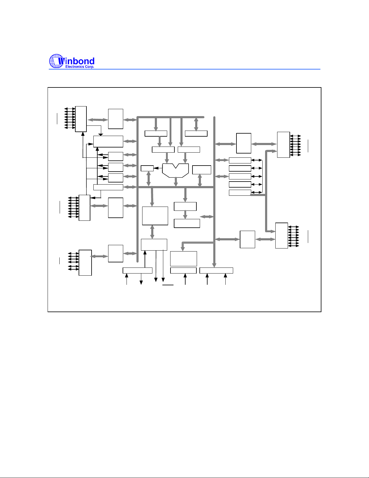
BLOCK DIAGRAM
W78LE812
P1.0
P1.7
P3.0
P3.7
P4.0
P4.6
Port
1
Port
Port
Port 1
Latch
INT2~9
Interrupt
Timer
2
Timer
0
Timer
1
UART
3
4
Port 3
Latch
Port 4
Latch
Oscillator
XTAL1
ACC
PSW
Instruction
Decoder
&
Sequencer
Bus & Clock
Controller
ALE
PSEN
ALU
SFR RAM
Address
256 bytes
RAM & SFR
Watchdog
Timer
Reset Block
B
Port 0
T2T1
Latch
Port
0
P0.0
P0.7
DPTR
Stack
Pointer
Temp Reg.
PC
Incrementor
Addr. Reg.
P2.0
Port 2
Latch
Port
2
P2.7
Power control
VssVCCRSTXTAL2
FUNCTIONAL DESCRIPTION
The W78LE812 architecture consists of a core controller surrounded by various registers, five general
purpose I/O ports, 256 bytes of RAM, three timer/counters, and a serial port. The processor supports
111 different opcodes and references both a 64K program address space and a 64K data storage
space.
Timers 0, 1, and 2
Timers 0, 1, and 2 each consist of two 8-bit data registers. These are called TL0 and TH0 for Timer 0,
TL1 and TH1 for Timer 1, TL2 and TH2 for Timer 2. The TCON and TMOD registers provide control
functions for timers 0 and 1. The T2CON register provides control functions for Timer 2. RCAP2H
and RCAP2L are used as reload/capture registers for Timer 2. The operations of Timer 0 and Timer 1
are the same as in the W78C51. Timer 2 is a special feature of the W78LE812: it is a 16-bit up/down
counter that is configured and controlled by the T2CON and T2MOD registers. Like Timers 0 and 1,
Timer 2 can operate as either an external event counter or as an internal timer, depending on the
- 4 -
W78LE812
setting of bit C/T2 in T2CON. Timer 2 has three operating modes: capture, auto-reload, and baud rate
generator. The clock speed at capture or auto-reload mode is the same as that of Timers 0 and 1. In
the auto-reload mode, Timer 2 performs a up counter which is similar with standard 8052. When
counting up, an overflow in Timer 2 will cause a reload from RCAP2H and RCAP2L registers. The
Timer 2 also provides a programmable clock-out mode as a clock generator. To enable this mode,
timer 2 has to be configured with a 16-bit auto-reload timer (C/T2 = 0, CP/RL2 = 0) and bit T2OE
(T2MOD.1) must be set to 1. This mode produces a 50% duty cycle clock output and timer 2 rollovers will not generate an interrupt. The clock-out frequency depends on the oscillator frequency and
the reload value of registers RCAP2H and RCAP2L. The clock-out frequency is determined by
following equation:
Clock-out Frequency = Oscillator Frequency / [ 4 × ( 65536 - RCAP2H, RCAP2L ) ]
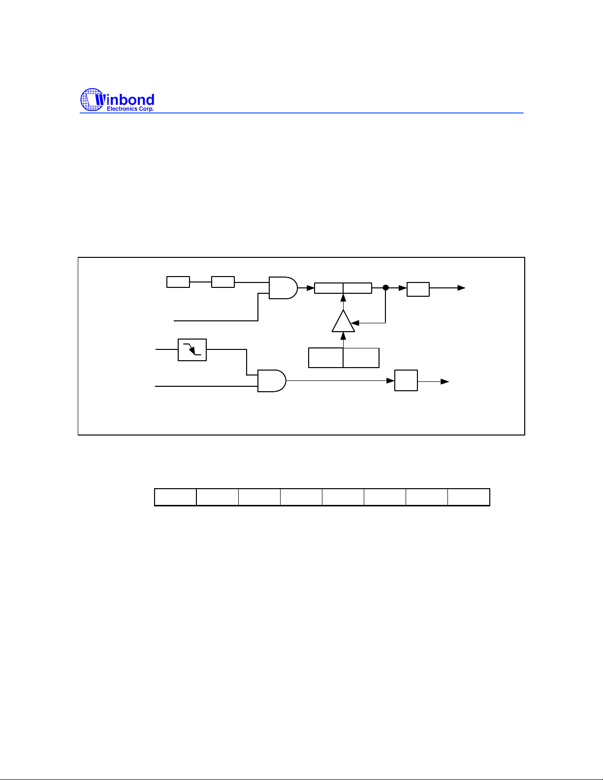
TR2 (T2CON.2)
T2EX (P1.1)
EXEN2 (T2CON.3)
OSC 1/2
RCAP2L
TH2TL2
RCAP2H
1/2
EXF2 Timer 2
Interrupt
T2CON.6
T2 (P1.0)
Timer 2 Clock-Out Mode
TIMER 2 MODE CONTROL
Bit: 7 6 5 4 3 2 1 0
- - - - - - T2OE Mnemonic: T2MOD Address: C9h
T2OE: Timer 2 Output Enable. This bit enables/disables the Timer 2 clock-out function.
I/O Port Options
The Port 0 and Port 3 of W78LE812 may be configured with different types by setting the bits of the
Port Options Register POR that is located at 86H. The pins of Port 0 can be configured with either
the open drain or standard port with internal pull-up. By the default, Port 0 is an open drain bidirectional I/O port. When the PUP bit in the POR register is set, the pins of Port 0 will perform a
quasi-bi-directional I/O port with internal pull-up that is structurally the same as Port 2. The high
nibble of Port 3 (P3.4 to P3.7) can be selected to serve the direct LED displays drive outputs by
setting the HDx bit in the PO register. When the HDx bit is set, the corresponding pin P3.x can sink
about 20mA current for driving LED display directly. After reset, the POR register is cleared and the
pins of Ports 0 and 3 are the same as those of the standard 80C31. The POR register is shown below.
Publication Release Date: February 1999
- 5 - Revision A2

W78LE812
INT
1
Port Options Register
Bit: 7 6 5 4 3 2 1 0
EP6 EP5 - HD7 HD6 HD5 HD4 PUP
Mnemonic: POR Address: 86H
PUP : Enable Port 0 weak pull-up.
HD4−7 : Enable pins P3.4 to P3.7 individually with High Drive outputs.
EP5 : Enable P4.5. To set this bit shifts ALE pin to the alternate function P4.5.
EP6 : Enable P4.6. To set this bit shifts PSEN pin to the alternate function P4.6
Port 4
The W78LE812 has one additional bit-addressable I/O port P4 in which the port address is D8H. The
Port 4 contains seven bits; P4.0 to P4.3 are only available on 44-pin PLCC/QFP package; P4.5 and
P4.6 are the alternate function corresponding to pins ALE, PSEN. When program is running in the
internal memory without any access to external memory, ALE and PSEN may be individually
configured to the alternate functions P4.5 and P4.6 that serve as general purpose I/O pins. To enable
I/O port P4.5 and P4.6, the bits EP5 and EP6 in the POR register must be set. During reset, the, ALE
and PSEN perform as in the standard 80C32. The alternate functions P4.5 and P4.6 must be
enabled by software. Care must be taken with the ALE pins when configured as the alternate
functions. The ALE will emit pulses until either the EP5 bit in POR register or AO bit in AUXR register
is set to 1. i.e. User's applications should elude the ALE pulses before software configure it with I/O
port P4.5.
Port 4
Bit: 7 6 5 4 3 2 1 0
- P4.6 P4.5 - P4.3 P4.2 P4.1 P4.0
Mnemonic: P4 Address: D8H
Interrupt System
The W78LE812 has twelve interrupt sources:
INT9. Each interrupt vectors to a specific location in program memory for its interrupt service routine.
Each of these sources can be individually enabled or disabled by setting or clearing the
corresponding bit in Special Function Register IE0 and IE1. The individual interrupt priority level
depends on the Interrupt Priority Register IP0 and IP1. Additional external interrupts INT2 to INT9 are
level sensitive and may be used to awake the device from power down mode. The Port 1 interrupts
can be initialized to either active HIGH or LOW via setting the Interrupt Polarity Register IX. The IRQ
register contains the flags of Port 1 interrupts. Each flag in IRQ register will be set when a interrupt
request is recognized but must be cleared by software. Note that the interrupt flags have to be
cleared before the interrupt service routine is completed, or else another interrupt will be generated.
INT0
- 6 -
and
; Timer 0,1 and 2; Serial Port; INT2 to

Interrupt Enable Register 0
Bit: 7 6 5 4 3 2 1 0
EA - ET2 ES ET1 EX1 ET0 EX0
Mnemonic: IE Address: A8H
EA : Global enable. Enable/disable all interrupts.
ET2: Enable Timer 2 interrupt.
ES : Enable Serial Port interrupt.
ET1: Enable Timer 1 interrupt
EX1: Enable external interrupt 1
ET0: Enable Timer 0 interrupt
EX0: Enable external interrupt 0
Interrupt Enable Register 1
Bit: 7 6 5 4 3 2 1 0
EX9 EX8 EX7 EX6 EX5 EX4 EX3 EX2
Mnemonic: IE1 Address: E8H
W78LE812
EX9: Enable external interrupt 9 Note: 0 = interrupt disabled, 1 = interrupt enabled.
EX8: Enable external interrupt 8
EX7: Enable external interrupt 7
EX6: Enable external interrupt 6
EX5: Enable external interrupt 5
EX4: Enable external interrupt 4
EX3: Enable external interrupt 3
EX2: Enable external interrupt 2
Interrupt Priority Register 0
Bit: 7 6 5 4 3 2 1 0
- PS1 PT2 PS PT1 PX1 PT0 PX0
Mnemonic: IP0 Address: B8h
IP.7: Unused.
PS1: This bit defines the Serial port 1 interrupt priority. PS = 1 sets it to higher priority level.
PT2: This bit defines the Timer 2 interrupt priority. PT2 = 1 sets it to higher priority level.
PS : This bit defines the Serial port 0 interrupt priority. PS = 1 sets it to higher priority level.
PT1: This bit defines the Timer 1 interrupt priority. PT1 = 1 sets it to higher priority level.
PX1: This bit defines the External interrupt 1 priority. PX1 = 1 sets it to higher priority level.
PT0: This bit defines the Timer 0 interrupt priority. PT0 = 1 sets it to higher priority level.
PX0: This bit defines the External interrupt 0 priority. PX0 = 1 sets it to higher priority level.
Publication Release Date: February 1999
- 7 - Revision A2

W78LE812
Interrupt Priority Register 1
Bit: 7 6 5 4 3 2 1 0
PX9 PX8 PX7 PX6 PX5 PX4 PX3 PX2
Mnemonic: IP1 Address: F8h
PX9: This bit defines the External interrupt 9 priority. PX9 = 1 sets it to higher priority level.
PX8: This bit defines the External interrupt 8 priority. PX8 = 1 sets it to higher priority level.
PX7: This bit defines the External interrupt 7 priority. PX7 = 1 sets it to higher priority level.
PX6: This bit defines the External interrupt 6 priority. PX6 = 1 sets it to higher priority level.
PX5: This bit defines the External interrupt 5 priority. PX5 = 1 sets it to higher priority level.
PX4: This bit defines the External interrupt 4 priority. PX4 = 1 sets it to higher priority level.
PX3: This bit defines the External interrupt 3 priority. PX3 = 1 sets it to higher priority level.
PX2: This bit defines the External interrupt 2 priority. PX2 = 1 sets it to higher priority level.
Interrupt Polarity Register
Bit: 7 6 5 4 3 2 1 0
IL9 IL8 IL7 IL6 IL5 IL4 IL3 IL2
Mnemonic: IX Address: E9H
IL9: External interrupt 9 polarity level.
IL8: External interrupt 8 polarity level.
IL7: External interrupt 7 polarity level.
IL6: External interrupt 6 polarity level.
IL5: External interrupt 5 polarity level.
IL4: External interrupt 4 polarity level.
IL3: External interrupt 3 polarity level.
IL2: External interrupt 2 polarity level.
Note: 0 = active LOW, 1 = active HIGH.
Interrupt Request Flag Register
Bit: 7 6 5 4 3 2 1 0
IQ9 IQ8 IQ7 IQ6 IQ5 IQ4 IQ3 IQ2
Mnemonic: IRQ Address: C0H
IQ9: External interrupt 9 request flag.
IQ8: External interrupt 8 request flag.
IQ7: External interrupt 7 request flag.
IQ6: External interrupt 6 request flag.
IQ5: External interrupt 5 request flag.
IQ4: External interrupt 4 request flag.
IQ3: External interrupt 3 request flag.
IQ2: External interrupt 2 request flag.
- 8 -
 Loading...