

Winbond Electronics W24512AJ-25, W24512AT-25, W24512AS-25 Datasheet
W24512A
2
3
5
6
789
10
1213141516
A3
I/O1
I/O2
V
OE
CS1
I/O7
I/O6
I/O3
DD
A9
28
CS1
WE
OE
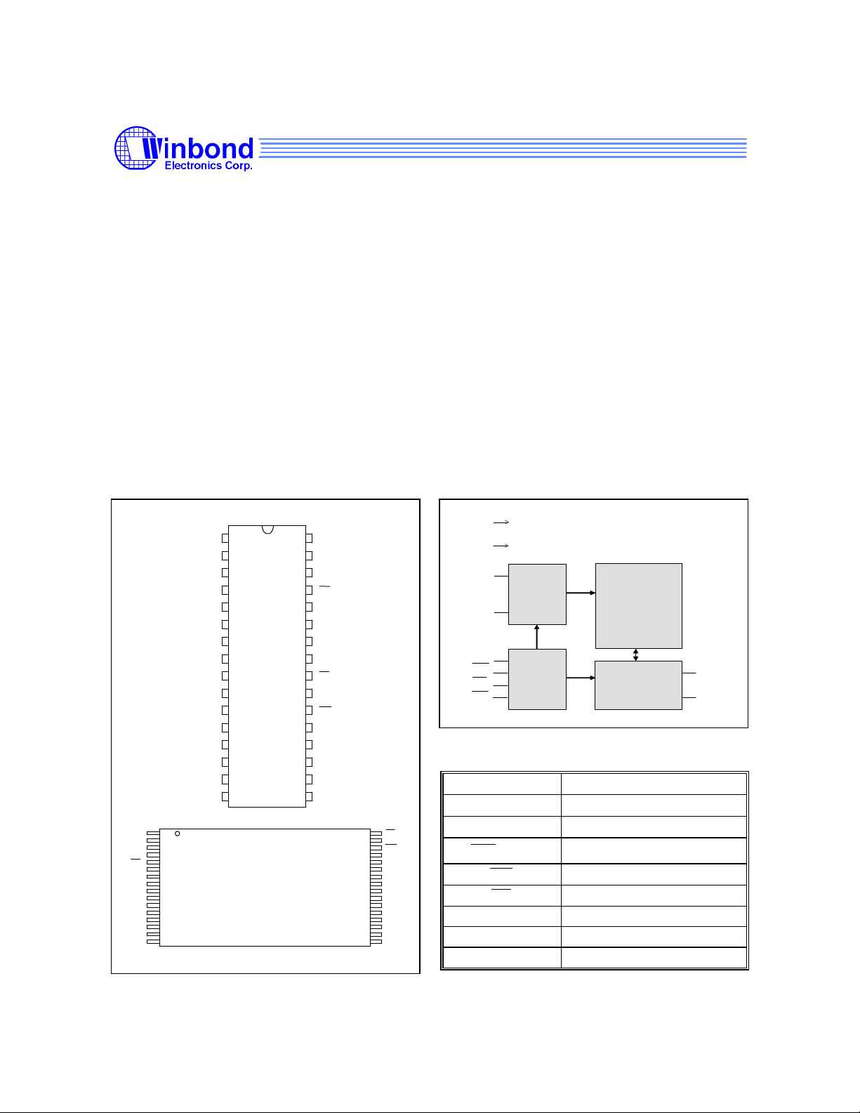
64K × 8 HIGH SPEED CMOS STATIC RAM
GENERAL DESCRIPTION
The W24512A is a high speed, low power CMOS static RAM organized as 65536 × 8 bits that
operates on a single 5-volt power supply. This device is manufactured using Winbond's high
performance CMOS technology.
FEATURES
• High speed access time: 25 nS (max.)
• Low power consumption:
− Active: 800 mW (max.)
• Single +5V power supply
• Fully static operation
PIN CONFIGURATIONS
32
1
NC
2
NC
A14
3
4
A12
A7
5
A6
6
A5
7
A4
8
A3
9
A2
10
A1
11
A0
12
I/O1
13
I/O2
14
I/O3
15
V
SS
16 17
A11
A8
4
A13
WE
CS2
A15
NC
NC
11
A14
A12
A7
A6
A5
A4
32-pin
TSOP
V
DD
31
A15
30
CS2
29
WE
A13
28
A8
27
A9
26
A11
25
24
OE
23
A10
22
CS1
21
I/O8
20
I/O7
I/O6
19
I/O5
18
I/O4
• All inputs and outputs directly TTL compatible
• Three-state outputs
• Available packages: 32-pin 300 mil SOJ, 450
mil SOP, and standard type one TSOP
(8 mm × 20 mm)
BLOCK DIAGRAM
V
DD
V
SS
A0
A15
.
.
DECODER
CORE
ARRAY
CS2
CS1
OE
WE
CONTROL
DATA I/O
I/O1
I/O8
.
.
PIN DESCRIPTION
SYMBOL DESCRIPTION
A0−A15
32
A10
31
30
I/O8
29
27
I/O5
26
I/O4
25
24
V
SS
23
22
21
A0
20
A1
19
18
A2
17
I/O1−I/O8
, CS2
VDD Power Supply
VSS Ground
NC No Connection
Address Inputs
Data Inputs/Outputs
Chip Select Inputs
Write Enable Input
Output Enable Input
Publication Release Date: April 1997
- 1 - Revision A3
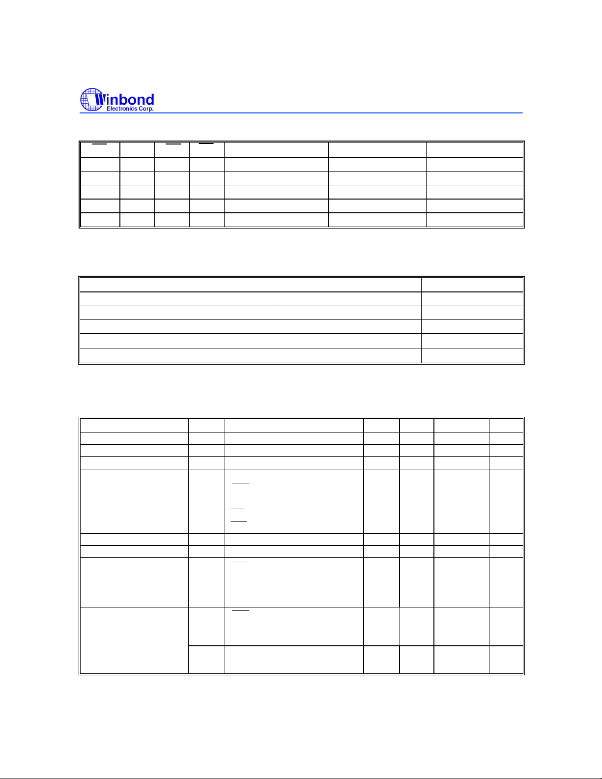
TRUTH TABLE
CS1
OE
WE
CS1
CS1
CS1
W24512A
CS1 CS2 OE WE MODE
H X X X Not Selected High Z ISB, ISB1
X L X X Not Selected High Z ISB, ISB1
L H H H Output Disable High Z IDD
L H L H Read Data Out IDD
L H X L Write Data In IDD
I/O1−I/O8
VDD CURRENT
DC CHARACTERISTICS
Absolute Maximum Ratings
PARAMETER RATING UNIT
Supply Voltage to VSS Potential -0.5 to +7.0 V
Input/Output to VSS Potential -0.5 to VDD +0.5 V
Allowable Power Dissipation 1.0 W
Storage Temperature -65 to +150
Operating Temperature 0 to +70
Note: Exposure to conditions beyond those listed under Absolute Maximum Ratings may adversely affect the life and reliability of the
device.
Operating Characteristics
(VDD = 5V ±10%, VSS = 0V, TA = 0 to 70° C)
PARAMETER SYM. TEST CONDITIONS MIN. TYP. MAX. UNIT
Input Low Voltage VIL - -0.5 - +0.8 V
Input High Voltage VIH - +2.2 - VDD +0.5 V
Input Leakage Current ILI VIN = VSS to VDD -10 - +10
Output Leakage
Current
Output Low Voltage VOL IOL = +8.0 mA - - 0.4 V
Output High Voltage VOH IOH = -4.0 mA 2.4 - - V
Operating Power
Supply Current IDD
Standby Power
Supply Current
Note: Typical characteristics are at VDD = 5V, TA = 25° C.
ILO VI/O = VSS to VDD
= VIH (min.) or
CS2 = VIL (max.) or
= VIH (min.) or
= VIL (max.)
= VIL (max.),
CS2 = VIH (min.)
I/O = 0mA, Cycle = min
Duty = 100%
ISB
ISB1
= VIH (min.) or
CS2 = VIL (max.)
Cycle = min, Duty = 100%
≥ VDD -0.2V or
CS2 ≤ 0.2V
-10 - +10
- - 160 mA
- - 30 mA
- - 10 mA
°C
°C
µA
µA
- 2 -
W24512A
CAPACITANCE
(VDD = 5V, TA = 25° C, f = 1 MHz)
PARAMETER SYM. CONDITIONS MAX. UNIT
Input Capacitance CIN VIN = 0V 8 pF
Input/Output Capacitance CI/O VOUT = 0V 10 pF
Note: These parameters are sampled but not 100% tested.
AC CHARACTERISTICS
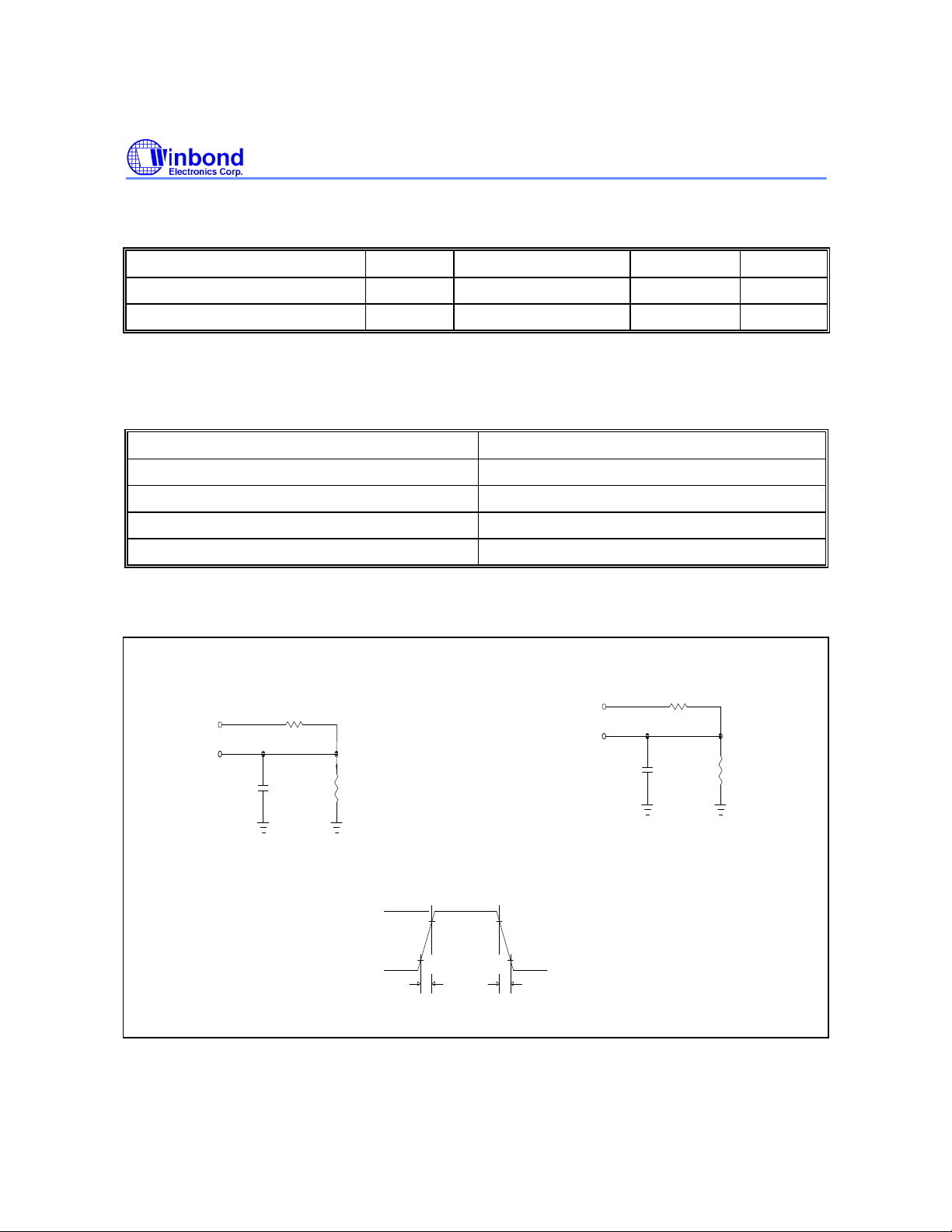
AC Test Conditions
PARAMETER CONDITIONS
Input Pulse Levels 0V to 3V
Input Rise and Fall Times 5 nS
Input and Output Timing Reference Level 1.5V
Output Load CL = 30 pF, IOH/IOL = -4 mA/8 mA
AC Test Loads and Waveform
R1 480 ohm
5V
OUTPUT
30 pF
Including
Jig and
Scope
R2
255 ohm
3.0V
0V
5 nS
(For T
90% 90%
10%
10%
OUTPUT
T
CLZ1, CLZ2,
5 nS
5V
T
OLZ,
T
R1 480 ohm
5 pF
Including
Jig and
Scope
T T
CHZ1, CHZ2, OHZ,
T T
WHZ,
R2
255 ohm
)
OW
Publication Release Date: April 1997
- 3 - Revision A3
 Loading...