

Page 1

NO: W90P710 Programming Guide VERSION: 2.1 PAGE: 1
W90P710 Programming Guide
Revision 2.1
01/06/2006
The above information is the exclusive intellectual property of Winbond Electronics and shall not be disclosed,
distributed or reproduced without permission from Winbond.
Table No.: 1200-0003-07-A
Page 2

NO: W90P710 Programming Guide VERSION: 2.1 PAGE: 2
Revision History
Revision Date Comment
1.0 08/30/2005 Initial Version for W90P710
2.0 Major Revision
2.1 01/06/2006 Modify some contents and re-order the
sections
The above information is the exclusive intellectual property of Winbond Electronics and shall not be disclosed,
distributed or reproduced without permission from Winbond.
Table No.: 1200-0003-07-A
Page 3

NO: W90P710 Programming Guide VERSION: 2.1 PAGE: 3
Table of Contents
1 Overview...................................................................................................................................... 15
1.1 Features ............................................................................................................................... 18
1.1.1 Architecture ................................................................................................................... 18
1.1.2 External Bus Interface ................................................................................................... 18
1.1.3 Instruction and Data Cache ........................................................................................... 18
1.1.4 Ethernet MAC Controller................................................................................................ 18
1.1.5 DMA Controller .............................................................................................................. 19
1.1.6 USB Host Controller ...................................................................................................... 19
1.1.7 USB Device Controller................................................................................................... 19
1.1.8 SDIO Host Controller..................................................................................................... 19
1.1.9 LCD Controller............................................................................................................... 20
1.1.10 2 Channel AC97/I2S Audio Codec Host Interface ......................................................... 21
1.1.11 UART............................................................................................................................. 21
1.1.12 Timers............................................................................................................................ 21
1.1.13 Advanced Interrupt Controller........................................................................................ 21
1.1.14 GPIO ............................................................................................................................. 22
1.1.15 Real Time Clock ............................................................................................................ 22
1.1.16 Smart Card Host Interface ............................................................................................. 22
1.1.17 I2C Master ..................................................................................................................... 23
1.1.18 Universal Serial Interface (USI) ..................................................................................... 23
1.1.19 4-Channel PWM ............................................................................................................ 23
1.1.20 Keypad Interface ........................................................................................................... 24
1.1.21 PS2 Host Interface Controller........................................................................................ 24
1.1.22 Power Management ...................................................................................................... 24
2 EBI (External Bus Interface) ........................................................................................................ 25
2.1 Overview............................................................................................................................... 25
2.2 Block Diagram ...................................................................................................................... 26
2.2.1 SDRAM interface........................................................................................................... 26
2.3 Registers .............................................................................................................................. 27
2.4 Functional Descriptions ........................................................................................................ 27
2.4.1 EBI Control Register (EBICON)..................................................................................... 27
The above information is the exclusive intellectual property of Winbond Electronics and shall not be disclosed,
distributed or reproduced without permission from Winbond.
Table No.: 1200-0003-07-A
Page 4

NO: W90P710 Programming Guide VERSION: 2.1 PAGE: 4
2.4.2 ROM/Flash control register............................................................................................ 28
2.4.3 SDRAM configuration registers ..................................................................................... 29
2.4.4 External I/O control registers ......................................................................................... 30
2.4.5 A system memory initialization example flow chart........................................................ 30
2.4.6 REMAPPING ................................................................................................................. 32
3 Cache Controller.......................................................................................................................... 35
3.1 Overview............................................................................................................................... 35
3.2 Block Diagram ...................................................................................................................... 36
3.3 Registers .............................................................................................................................. 38
3.4 Functional Descriptions ........................................................................................................ 38
3.4.1 On-Chip RAM ................................................................................................................ 38
3.4.2 Non-Cacheable Area ..................................................................................................... 39
3.4.3 Cache Flushing.............................................................................................................. 39
3.4.4 Cache Enable and Disable ............................................................................................ 39
3.4.5 Cache Load and Lock.................................................................................................... 40
3.4.6 Cache Unlock ................................................................................................................ 41
4 EMC (Ethernet MAC Controller) .................................................................................................. 42
4.1 Overview............................................................................................................................... 42
4.2 Block Diagram ...................................................................................................................... 43
4.3 Registers .............................................................................................................................. 44
4.3.1 EMC Control registers .................................................................................................. 44
4.3.2 EMC Status Registers ................................................................................................... 45
4.4 Functional Descriptions ........................................................................................................
45
4.4.1 Initialize Rx Buffer Descriptors....................................................................................... 45
4.4.2 Initialize Tx Buffer Descriptors ....................................................................................... 48
4.4.3 MII ................................................................................................................................. 50
4.4.4 Control Frames.............................................................................................................. 52
4.4.5 Packet Processing......................................................................................................... 52
5 GDMA .......................................................................................................................................... 58
5.1 Overview............................................................................................................................... 58
5.2 Block Diagram ...................................................................................................................... 59
5.3 Registers .............................................................................................................................. 60
5.4 Functional Descriptions ........................................................................................................ 60
The above information is the exclusive intellectual property of Winbond Electronics and shall not be disclosed,
distributed or reproduced without permission from Winbond.
Table No.: 1200-0003-07-A
Page 5

NO: W90P710 Programming Guide VERSION: 2.1 PAGE: 5
5.4.1 GDMA Configuration ..................................................................................................... 60
5.4.2 Transfer Count............................................................................................................... 62
5.4.3 Transfer Termination ..................................................................................................... 63
5.4.4 GDMA operation started by software............................................................................. 63
5.4.5 GDMA operation started by nXDREQ ........................................................................... 65
5.4.6 Fixed Address................................................................................................................ 66
5.4.7 Block Mode Transfer ..................................................................................................... 66
5.4.8 Single Mode Transfer .................................................................................................... 66
5.4.9 Demand Mode Transfer................................................................................................. 66
6 USB Host Controller..................................................................................................................... 68
6.1 Overview............................................................................................................................... 68
6.2 Registers Map....................................................................................................................... 69
6.3 Block Diagram ...................................................................................................................... 70
6.4 Data Structures..................................................................................................................... 71
6.4.1 Endpoint Descriptor (ED) Lists ...................................................................................... 72
6.4.2 Transfer Descriptor........................................................................................................ 73
6.4.3 Host Controller Communication Area ............................................................................ 75
6.5 Programming Note................................................................................................................76
6.5.1 Initialization.................................................................................................................... 76
6.5.2 USB States .................................................................................................................... 77
6.5.3 Add/Remove Endpoint Descriptors................................................................................ 78
6.5.4 Add/Remove Transfer Descriptors ................................................................................ 80
6.5.5 IRP Processing.............................................................................................................. 82
6.5.6 Interrupt Processing ...................................................................................................... 84
6.5.7 Done Queue Processing................................................................................................ 88
6.5.8 Root Hub ....................................................................................................................... 90
7 USB Device Controller ................................................................................................................. 94
7.1 Overview............................................................................................................................... 94
7.2 Block Diagram ...................................................................................................................... 95
7.3 Register Map ........................................................................................................................ 95
7.4 Functional descriptions .........................................................................................................97
7.4.1 Initialization.................................................................................................................... 97
7.4.2 Endpoint Configuration .................................................................................................. 98
The above information is the exclusive intellectual property of Winbond Electronics and shall not be disclosed,
distributed or reproduced without permission from Winbond.
Table No.: 1200-0003-07-A
Page 6

NO: W90P710 Programming Guide VERSION: 2.1 PAGE: 6
7.4.3 Interrupt Service Routine............................................................................................... 98
7.4.4 Endpoint 0 Operation..................................................................................................... 99
7.4.5 Get Descriptor ............................................................................................................. 100
7.4.6 Endpoint A ~ C Operation............................................................................................ 101
7.4.7 Example....................................................................................................................... 102
8 SDIO Host Controller ................................................................................................................. 103
8.1 Overview............................................................................................................................. 103
8.2 Block Diagram .................................................................................................................... 103
8.3 Registers ............................................................................................................................ 104
8.4 SDIO Host Controller .......................................................................................................... 105
8.4.1 SDIO host controller Initialization Sequence................................................................ 105
8.4.2 Move data from SDRAM to SDIO host controller buffer .............................................. 106
8.4.3 Move data from SDIO host controller buffer to SDRAM .............................................. 106
8.5 SD Host Interface ............................................................................................................... 106
8.5.1 Send Command to SD/MMC Card .............................................................................. 106
8.5.2 Get Response from SD/MMC Card ............................................................................. 107
8.5.3 SD/MMC to Buffer Access ........................................................................................... 107
8.5.4 Buffer to SD/MMC Access ........................................................................................... 107
9 LCD Controller ........................................................................................................................... 108
9.1.1 Overview...................................................................................................................... 108
9.1.2 Programming Procedure.............................................................................................. 112
9.2 Initialization......................................................................................................................... 115
9.3
Configure LCD Controller ................................................................................................... 115
9.4 Configure LCD Interrupt...................................................................................................... 117
9.5 Configure LCD Timing Generation...................................................................................... 117
9.6 Configure OSD function...................................................................................................... 117
9.7 Configure TFT Palette Look-up Table................................................................................. 119
9.8 Configure Gray level dithered data duty pattern ................................................................. 120
9.9 Configure Video/ OSD scaling factor .................................................................................. 120
9.10 Configure the starting address and the stride of frame buffer and FIFO............................. 121
9.11 Configure how to show image on the panel........................................................................ 124
9.12 Enable FIFO ....................................................................................................................... 125
9.13 Enable LCD Controller........................................................................................................ 126
The above information is the exclusive intellectual property of Winbond Electronics and shall not be disclosed,
distributed or reproduced without permission from Winbond.
Table No.: 1200-0003-07-A
Page 7

NO: W90P710 Programming Guide VERSION: 2.1 PAGE: 7
9.14 Check running state and process interrupt status............................................................... 126
10 Audio Controller...................................................................................................................... 128
10.1 Overview............................................................................................................................. 128
10.2 Block Diagram .................................................................................................................... 129
10.3 Registers ............................................................................................................................ 130
10.4 AC97 Interface.................................................................................................................... 130
10.4.1 Cold Reset External AC97 Codec ............................................................................... 132
10.4.2 Read AC97 Registers .................................................................................................. 132
10.4.3 Write AC97 Registers .................................................................................................. 134
10.4.4 AC97 Playback ............................................................................................................ 135
10.4.5 AC97 Record ............................................................................................................... 137
10.5 I2S Interface ....................................................................................................................... 138
10.5.1 I2S Play ....................................................................................................................... 138
10.5.2 I2S Record................................................................................................................... 140
11 UART ..................................................................................................................................... 142
11.1 Overview............................................................................................................................. 142
11.2 Registers ............................................................................................................................ 142
11.3 Functional Descriptions ...................................................................................................... 144
11.3.1 Baud Rate.................................................................................................................... 144
11.3.2 Initializations ................................................................................................................ 145
11.3.3 Polled I/O Functions .................................................................................................... 147
11.3.4
Interrupted I/O Functions ............................................................................................. 148
11.3.5 IrDA SIR ...................................................................................................................... 153
12 Timers .................................................................................................................................... 154
12.1 Overview............................................................................................................................. 154
12.2 Block Diagram .................................................................................................................... 155
12.3 Registers ............................................................................................................................ 155
12.4 Functional Descriptions ...................................................................................................... 156
12.4.1 Interrupt Frequency ..................................................................................................... 156
12.4.2 Initialization.................................................................................................................. 156
12.4.3 Timer Interrupt Service Routine................................................................................... 159
12.4.4 Watchdog Timer .......................................................................................................... 160
13 AIC (Advanced Interrupt Controller) ....................................................................................... 163
The above information is the exclusive intellectual property of Winbond Electronics and shall not be disclosed,
distributed or reproduced without permission from Winbond.
Table No.: 1200-0003-07-A
Page 8

NO: W90P710 Programming Guide VERSION: 2.1 PAGE: 8
13.1 Overview............................................................................................................................. 163
13.2 Block Diagram .................................................................................................................... 164
13.3 Registers ............................................................................................................................ 165
13.4 Functional Descriptions ...................................................................................................... 167
13.4.1 Interrupt channel configuration .................................................................................... 167
13.4.2 Interrupt Masking ......................................................................................................... 167
13.4.3 Interrupt Clearing and Setting...................................................................................... 168
13.4.4 Software Priority Scheme ............................................................................................ 168
13.4.5 Hardware Priority Scheme........................................................................................... 171
14 General-Purpose Input/Output (GPIO) ................................................................................... 174
14.1 Overview............................................................................................................................. 174
14.2 Register Map ...................................................................................................................... 176
14.3 Functional Description ........................................................................................................ 177
14.3.1 Multiple Functin Setting ............................................................................................... 177
14.3.2 GPIO Output Mode ...................................................................................................... 178
14.3.3 GPIO Input Mode......................................................................................................... 179
15 Real Time Clock (RTC) .......................................................................................................... 181
15.1 Overview............................................................................................................................. 181
15.2 Block Diagram .................................................................................................................... 182
15.3 Register Map ...................................................................................................................... 182
15.4 Functional Description ........................................................................................................ 183
15.4.1 Initialization.................................................................................................................. 183
15.4.2 RTC Read/Write Enable .............................................................................................. 183
15.4.3 Frequency Compensation............................................................................................ 183
15.4.4 Application Note .......................................................................................................... 184
15.5 Programming Note.............................................................................................................. 185
15.5.2 Set Calendar and Time Alarm ..................................................................................... 187
15.5.3 Set tick interrupt........................................................................................................... 189
16 Smart Card Host Interface...................................................................................................... 191
16.1 Overview............................................................................................................................. 191
16.2 Registers ............................................................................................................................ 191
16.3 Functional Description ........................................................................................................ 193
16.3.1 Initialization Sequence................................................................................................. 193
The above information is the exclusive intellectual property of Winbond Electronics and shall not be disclosed,
distributed or reproduced without permission from Winbond.
Table No.: 1200-0003-07-A
Page 9

NO: W90P710 Programming Guide VERSION: 2.1 PAGE: 9
16.3.2 Timers Usage .............................................................................................................. 194
16.3.3 Receiver FIFO Data Time-out...................................................................................... 196
16.3.4 Parity Error management............................................................................................. 197
2
17 I
C Synchronous Serial Interface Controller........................................................................... 199
17.1 Overview............................................................................................................................. 199
17.2 Block Diagram .................................................................................................................... 201
17.3 Register Map ...................................................................................................................... 201
17.4 Functional Description ........................................................................................................ 202
17.4.1 Prescale Frequency..................................................................................................... 202
17.4.2 Start and Stop Signal................................................................................................... 202
17.4.3 Slave Address Transfer ............................................................................................... 202
17.4.4 Data Transfer............................................................................................................... 203
17.4.5 Below list Some Examples of I2C Data Transaction.................................................... 203
18 Universal Serial Interface ....................................................................................................... 209
18.1 Overview............................................................................................................................. 209
18.2 Block Diagram .................................................................................................................... 210
18.3 Register Map ...................................................................................................................... 210
18.4 Functional Description ........................................................................................................ 211
18.4.1 Active Universal Serial Interface.................................................................................. 211
18.4.2 Initialize Universal Serial Interface............................................................................... 211
18.4.3 Universal Serial Interface Transmit/Receive................................................................ 212
19 Pulse Width Modulation (PWM) Timer ................................................................................... 213
19.1 Overview............................................................................................................................. 213
19.2 Block Diagram .................................................................................................................... 215
19.3 Register Map ...................................................................................................................... 215
19.4 Functional Description ........................................................................................................ 2
16
19.4.1 Prescaler and clock selector........................................................................................ 216
19.4.2 Basic PWM timer operation and double buffering reload automatically....................... 217
19.4.3 PWM Timer Start Procedure........................................................................................ 218
19.4.4 PWM Timer Stop Procedure........................................................................................ 220
20 Keypad Interface .................................................................................................................... 222
20.1 Overview............................................................................................................................. 222
20.2 Block Diagram .................................................................................................................... 223
The above information is the exclusive intellectual property of Winbond Electronics and shall not be disclosed,
distributed or reproduced without permission from Winbond.
Table No.: 1200-0003-07-A
Page 10

NO: W90P710 Programming Guide VERSION: 2.1 PAGE: 10
20.3 Register Map ...................................................................................................................... 223
20.4 Functional Description ........................................................................................................ 223
20.4.1 KPI Interface Programming Flow................................................................................. 224
20.4.2 KPI Low Power Mode Configuration ............................................................................ 225
21 PS/2 Host Interface Controller................................................................................................ 227
21.1 Overview............................................................................................................................. 227
21.2 Scan Code Set.................................................................................................................... 227
21.3 Register Map ...................................................................................................................... 229
21.4 Functional Description ........................................................................................................ 229
21.4.1 Initialization.................................................................................................................. 229
21.4.2 Send Commands ......................................................................................................... 230
21.4.3 Read scan code and ASCII code................................................................................. 231
21.4.4 Interrupt Service Routine ............................................................................................. 232
21.4.5 Example....................................................................................................................... 235
The above information is the exclusive intellectual property of Winbond Electronics and shall not be disclosed,
distributed or reproduced without permission from Winbond.
Table No.: 1200-0003-07-A
Page 11

NO: W90P710 Programming Guide VERSION: 2.1 PAGE: 11
Table of Figures
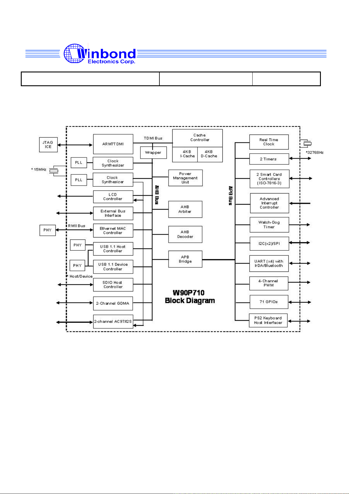
Figure 1-1 W90P710 Functional Block Diagram ................................................................................ 16
Figure 2-1 SDRAM Interface............................................................................................................... 26
Figure 2-2 System Memory Map Setting Flow .................................................................................... 30
Figure 3-1 Instruction Cache Organization Block Diagram ................................................................. 36
Figure 3-2 Data Cache Organization Block Diagram .......................................................................... 37
Figure 3-3 Cache Load and Lock........................................................................................................ 40
Figure 4-1 EMC Block Diagram .......................................................................................................... 43
Figure 4-2 Rx Descriptor Initialization ................................................................................................. 47
Figure 4-3 Tx Descriptor Initialization.................................................................................................. 49
Figure 4-4 Packet Transmission Flow................................................................................................. 53
Figure 4-5 Tx Interrupt Service Routine Flow...................................................................................... 55
Figure 4-6 Rx Interrupt Service Routine.............................................................................................. 57
Figure 5-1 GDMA Block Diagram........................................................................................................ 59
Figure 5-2 The bit-fields of the GDMA control register........................................................................ 61
Figure 5-3 GDMA operations .............................................................................................................. 62
Figure 5-4 Software GDMA Transfer................................................................................................... 64
Figure 6-1 Endpoint Descriptor Format............................................................................................... 72
Figure 6-2 General Transfer Descriptor Format .................................................................................. 74
Figure 6-3 Isochronous Transfer Descriptor Format ........................................................................... 74
Figure 6-4 Remove an Endpoint Descriptor ........................................................................................79
Figure 6-5 ED list and TD queue......................................................................................................... 80
Figure 7-1 USBD Controller Block Diagram ........................................................................................95
Figure 10-2 USBD Controller Block Diagram...................................................................................... 99
Figure 8-1 SDIO Host Block Diagram ............................................................................................... 103
Figure 9-1 LCD Controller Block Diagram......................................................................................... 108
Figure 9-2 Overall programming flow for LCD controller - 1.............................................................. 112
Figure 9-3 Overall programming flow for LCD controller - 2.............................................................. 114
Figure 9-4 The relationship between screen, valid window, and OSD window ................................. 117
Figure 9-5 An example to explain how to program the starting address and stride........................... 122
Figure 10-1 Block diagram of Audio Controlle................................................................................... 129
Figure 10-2 AC97 Playback Data in DMA Buffer .............................................................................. 135
The above information is the exclusive intellectual property of Winbond Electronics and shall not be disclosed,
distributed or reproduced without permission from Winbond.
Table No.: 1200-0003-07-A
Page 12

NO: W90P710 Programming Guide VERSION: 2.1 PAGE: 12
Figure 10-3 AC97 Data in Record DMA buffer.................................................................................. 137
Figure 10-4 I2S Play Data in DMA buffer.......................................................................................... 139
Figure 10-5 I2S Record Data in DMA buffer ..................................................................................... 140
Figure 11-1 UART initialization ......................................................................................................... 145
Figure 11-2 Transmit data in polling mode........................................................................................ 147
Figure 11-3 Receive data in polling mode......................................................................................... 148
Figure 11-4 Output function in interrupt mode................................................................................... 149
Figure 11-5 Input functions in interrupt mode.................................................................................... 150
Figure 11-6 Interrupt Service Routine ............................................................................................... 152
Figure 11-7 IrDA Tx/Rx ..................................................................................................................... 153
Figure 12-1 Timer Block Diagram ..................................................................................................... 155
Figure 12-2 Timer Initialization Sequence......................................................................................... 158
Figure 12-3 Timer Interrupt Service Routine ..................................................................................... 159
Figure 12-4 Enable Watchdog Timer ................................................................................................ 161
Figure 12-5 Watchdog Timer ISR ..................................................................................................... 162
Figure 13-1 AIC block diagram ......................................................................................................... 164
Figure 13-2 Source Control Register ................................................................................................ 167
Figure 13-3 Sequential Priority Scheme............................................................................................ 170
Figure 13-4 Interrupt Service Routine with Vector ............................................................................ 172
Figure 13-5 Using hardware priority scheme .................................................................................... 173
Figure 15-1 RTC Block Diagram ....................................................................................................... 182
Figure 15-2 RTC Set Calendar and Time flow chart ......................................................................... 186
Figure 15-3 RTC Set Calendar and Time Alarm flow chart ............................................................... 188
Figure 15-4 RTC Set tick interrupt flow chart .................................................................................... 189
2
Figure 17-1 I
C Block Diagram ......................................................................................................... 201
Figure 18-1 Universal Serial InterfaceI Block Diagra ........................................................................ 210
Figure 19-1 PWM Block Diagram...................................................................................................... 215
Figure 19-2 PWM operation .............................................................................................................. 218
Figure 19-3 PWM Timer Start Procedure.......................................................................................... 219
Figure 19-4 PWM Timer Stop flow chart (method 1)......................................................................... 220
Figure 19-5 PWM Timer Stop flow chart (method 2)......................................................................... 221
Figure 20-1 Keypad Controller Block Diagram.................................................................................. 223
Figure 20-2 KPI Interface flowchart................................................................................................... 225
The above information is the exclusive intellectual property of Winbond Electronics and shall not be disclosed,
distributed or reproduced without permission from Winbond.
Table No.: 1200-0003-07-A
Page 13

NO: W90P710 Programming Guide VERSION: 2.1 PAGE: 13
Figure 20-3 KPI set Wake-Up in system low power mode flowchart................................................. 226
Figure 21-1 Key map of PS/2 keyboard ............................................................................................ 227
Figure 21-2 Key map of extended keyboard & Numeric keypad ....................................................... 228
Figure 21-3 Make Code and Break Code.......................................................................................... 229
Figure 21-4 Example ISR.................................................................................................................. 233
The above information is the exclusive intellectual property of Winbond Electronics and shall not be disclosed,
distributed or reproduced without permission from Winbond.
Table No.: 1200-0003-07-A
Page 14

NO: W90P710 Programming Guide VERSION: 2.1 PAGE: 14
List of Tables
Table 3-1 The size and start address of On-Chip RAM ...................................................................... 38
Table 6-1 HCCA (Host Controller Communication Area) .................................................................... 75
Table 9-1 LCD Controller Register Map............................................................................................ 110
Table 9-2 Register LCDCON Bit Map ............................................................................................... 115
Table 9-3 OSD Display Condition ..................................................................................................... 118
Table 9-4 entry of the TFT Look-up table.......................................................................................... 119
Table 9-5 STN 16-leve gray number & relative Time-based dithering .............................................. 120
Table 9-6 BSWP=0, HSWP=0 .......................................................................................................... 125
Table 9-7 BSWP=0, HSWP=1 .......................................................................................................... 125
Table 9-8 BSWP=0, HSWP=0 .......................................................................................................... 125
Table 9-9 BSWP=1, HSWP=0 .......................................................................................................... 126
Table 10-1 AC97 Output Frame........................................................................................................ 131
Table 10-2 AC97 Output Frame Data Format ................................................................................... 131
Table 10-3 AC97 Input Frame........................................................................................................... 131
Table 10-4 AC97 Input Frame Data Format...................................................................................... 132
Table 11-1 General Baud Rate Settings ........................................................................................... 145
Table 12-1 Timer Reference Setting Values ..................................................................................... 156
Table 13-1 AIC Register Definition.................................................................................................... 165
Table 14-1 GPIO Multiplexed Functions Table ................................................................................. 174
Table 21-1 Command register PS2CMD........................................................................................... 230
Table 21-2 Command table............................................................................................................... 230
Table 21-3 Register PS2SCANCODE .............................................................................................. 231
Table 21-4 Register PS2ASCII ......................................................................................................... 232
Table 21-5 Register PS2ST .............................................................................................................. 232
Table 21-6 LED Status byte .............................................................................................................. 235
The above information is the exclusive intellectual property of Winbond Electronics and shall not be disclosed,
distributed or reproduced without permission from Winbond.
Table No.: 1200-0003-07-A
Page 15

NO: W90P710 Programming Guide VERSION: 2.1 PAGE: 15
1 Overview
The W90P710 16/32-bit RISC micro-controller is a cost-effective, high-performance micro-controller
solution for Ethernet-based system. An integrated Ethernet controller, the W90P710, is designed for
use in managed communication hubs and routers.
The W90P710 is built around an outstanding CPU core: on the 16/32 ARM7TDMI based RISC
processor designed by Advanced RISC Machines, Ltd. The ARM7TDMI core is a low power, general-
purpose integrated circuits. Its simple, elegant, and fully static design is particularly suitable for cost-
sensitive and power-sensitive applications.
The W90P710 offers a 4K-byte I-cache/SRAM, a 4K-byte D-cache/SRAM and one MACs of
Ethernet controller that reduces total system cost. A color LCD controller is built in to support black-and-
white/gray-level/color TFT and low cost STN LCD modules. Most of the on-chip function blocks have
been designed using an HDL synthesizer and the W90P710 has been fully verified in Winbond’s state-
of-the art ASIC test environment.
The other important peripheral functions include one USB host controller, one USB device
controller, one AC97/IIS codec controller, one SD/SDIO host controller, one 2-Channel GDMA, two
smartcard host controller, four independent UARTS, one Watchdog timer, two 24-bit timers with 8-bit
pre-scale, 71 programmable I/O ports, PS/2 keyboard controller and an advance interrupt controller.
The external bus interface (EBI) controller provides for SDRAM, ROM/SRAM, flash memory and I/O
devices. The System Manager includes an internal 32-bit system bus arbiter and a PLL clock controller.
The above information is the exclusive intellectual property of Winbond Electronics and shall not be disclosed,
distributed or reproduced without permission from Winbond.
Table No.: 1200-0003-07-A
Page 16
NO: W90P710 Programming Guide VERSION: 2.1 PAGE: 16
Figure 1-1 W90P710 Functional Block Diagram
On the following chapters, programming note of each chapter will be described in detailed.
• Chapter 2. External Bus Interface Controller
• Chapter 3. Cache Controller
• Chapter 4. Ethernet MAC Controller
• Chapter 5. GDMA
• Chapter 6. USB Host Controller
• Chapter 7. USB Device Controller
The above information is the exclusive intellectual property of Winbond Electronics and shall not be disclosed,
distributed or reproduced without permission from Winbond.
Table No.: 1200-0003-07-A
Page 17

NO: W90P710 Programming Guide VERSION: 2.1 PAGE: 17
• Chapter 8. SDIO Host Controller
• Chapter 9. LCD Controller
• Chapter 10. Audio Controller
• Chapter 11. UART
• Chapter 12. Timers
• Chapter 13. Advance Interrupt Controller
• Chapter 14. GPIO
• Chapter 15. Real Time Clock
• Chapter 16. Smartcard Host Interface Controller
• Chapter 17. I2C Synchronous Serial Interface
• Chapter 18. Universal Serial Interface
• Chapter 19. PWM-Tmer
• Chapter 20. Keypad Interface
• Chapter 21. PS/2 Host Interface Controller
The above information is the exclusive intellectual property of Winbond Electronics and shall not be disclosed,
distributed or reproduced without permission from Winbond.
Table No.: 1200-0003-07-A
Page 18

NO: W90P710 Programming Guide VERSION: 2.1 PAGE: 18
1.1 Features
1.1.1 Architecture
• Integrated system for POS (Point of Sale) and automatic data collection applications
• Fully 16/32-bit RISC architecture
• Little/Big-Endian mode supported
• Efficient and powerful ARM7TDMI core
• Cost-effective JTAG-based debug solution
1.1.2 External Bus Interface
• 8/16/32-bit external bus support for ROM/SRAM, flash memory, SDRAM and external I/Os
• Support for SDRAM
• Programmable access cycle (0-7 wait cycle)
• Four-word depth write buffer
• Cost-effective memory-to-peripheral DMA interface
1.1.3 Instruction an d Dat a Cache
• Two-way, Set-associative, 4K-byte I-cache and 4K-byte D-cache
• Support for LRU (Least Recently Used) Protocol
• Cache is configurable as an internal SRAM
• Support Cache Lock function
1.1.4 Ethernet MAC Controller
• DMA engine with burst mode
• MAC Tx/Rx buffers (256 bytes Tx, 256 bytes Rx)
• Data alignment logic
• Endian translation
• 100/10-Mbit per second operation
• Full compliance with IEEE standard 802.3
• RMII interface only
• Station Management Signaling
The above information is the exclusive intellectual property of Winbond Electronics and shall not be disclosed,
distributed or reproduced without permission from Winbond.
Table No.: 1200-0003-07-A
Page 19

NO: W90P710 Programming Guide VERSION: 2.1 PAGE: 19
• On-Chip CAM (up to 16 destination addresses)
• Full-duplex mode with PAUSE feature
• Long/short packet modes
• PAD generation
1.1.5 DMA Controller
• 2-channel General DMA for memory-to-memory data transfers without CPU intervention
• Initialed by a software or external DMA request
• Increments or decrements a source or destination address in 8-bit, 16-bit or 32-bit data transfers
• 4-data burst mode
1.1.6 USB Host Controller
• USB 1.1 compliant
• Compatible with Open HCI 1.0 specification
• Supports low-speed and full speed devices
• Build-in DMA for real time data transfer
• Two on-chip USB transceivers with one optionally shared with USB Device Controller
1.1.7 USB Device Controller
• USB 1.1 compliant
• Support four USB pipes including one control pipe and 3 configurable pipes for rich USB
functions
• Support USB Mass Storage
• Support USB Virtual COM port with modem capability
• Support Full speed only
1.1.8 SDIO Host Controller
• Directly connect to Secure Digital (SD, MMC or SDIO) flash memory card
• Supports DMA function to accelerate the data transfer between the internal buffer,
external SDRAM, and flash memory card
The above information is the exclusive intellectual property of Winbond Electronics and shall not be disclosed,
distributed or reproduced without permission from Winbond.
Table No.: 1200-0003-07-A
Page 20

NO: W90P710 Programming Guide VERSION: 2.1 PAGE: 20
• Two 512 bytes internal buffers are embedded inside of the controller
• No SPI mode
1.1.9 LCD Controller
• STN LCD Display
Supports Sync-type STN LCD
Supports 2 types of LCD panels: 4-bit single scan and 8-bit single scan display type
Supports 16 gray levels for Monochrome STN LCD panel
Supports 4096(12bpp) color for Color STN LCD panel
Virtual coloring method: Frame Rate Control (16-level)
Anti-flickering method: Time-based Dithering
• TFT LCD Display
Supports Sync-type TFT LCD and Sync-type High-color TFT LCD
Supports 8-bpp(RGB 332) palette color display
Supports 16-bpp(RGB 565) non-palette true color display
• TV Encoder
Supports 8-bit YCbCr data output format to connect with external TV Encoder
• LCD Prep ro ce ss ing
Image re-size
Horizontal/Vertical Down-Scaling
Horizontal/Vertical Up-Scaling
Image relocation
Horizontal /Vertical Cropping
Virtual Display
• LCD Postprocessing
Support for one OSD overlay
Support various OSD function
• Others
Color-look up table size 256x32 bit for TFT used
Dedicated DMA for block transfer mode
The above information is the exclusive intellectual property of Winbond Electronics and shall not be disclosed,
distributed or reproduced without permission from Winbond.
Table No.: 1200-0003-07-A
Page 21

NO: W90P710 Programming Guide VERSION: 2.1 PAGE: 21
1.1.10 2 Channel AC97/I2S Audio Codec Host Interface
• AHB master port and an AHB slave port are offered in audio controller
• Always 8-beat incrementing burst
• Always bus lock when 8-beat incrementing burst
• When reach middle and end address of destination address, a DMA_IRQ is
requested to CPU automatically
1.1.11 UART
• Four UART (serial I/O) blocks with interrupt-based operation
• Support for 5-bit, 6-bit, 7-bit or 8-bit serial data transmit and receive
• Programmable baud rates
• 1, ½ or 2 stop bits
• Odd or even parity
• Break generation and detection
• Parity, overrun and framing error detection
• X16 clock mode
• Support for Bluetooth, IrDA and Micro-printer control
1.1.12 Timers
• Two programmable 24-bit timers with 8-bit pre-scalar
• One programmable 24-bit Watch-Dog timer
• One-short mode, period mode or toggle mode operation
1.1.13 Advanced Interrupt Controller
• 31 interrupt sources, including 4 external interrupt sources
• Programmable normal or fast interrupt mode (IRQ, FIQ)
• Programmable as either edge-triggered or level-sensitive for 4 external interrupt sources
• Programmable as either low-active or high-active for 4 external interrupt sources
• Priority methodology is encoded to allow for interrupt daisy-chaining
• Automatically mask out the lower priority interrupt during interrupt nesting
• Automatically clear the interrupt flag when the interrupt source is programmed to be edge-
triggered
The above information is the exclusive intellectual property of Winbond Electronics and shall not be disclosed,
distributed or reproduced without permission from Winbond.
Table No.: 1200-0003-07-A
Page 22

NO: W90P710 Programming Guide VERSION: 2.1 PAGE: 22
1.1.14 GPIO
• 71 programmable I/O ports
• Pins individually configurable to input, output, or I/O mode for dedicated signals
• I/O ports Configurable for Multiple functions
1.1.15 Real Time Clock
• Time counter (second, minute, hour) and calendar counter (day, month, year)
• Alarm register (second, minute, hour, day, month, year)
• 12 or 24-hour mode selectable
• Recognize leap year automatically
• Day of the week counter
• Frequency compensate register (FCR)
• Beside FCR, all clock and alarm data expressed in BCD code
• Support tick time interrupt
1.1.16 Smart Card Host Interface
• ISO-7816 compliant
• PC/SC T=0, T=1 compliant
16-byte transmitter FIFO and 16-byte receiver FIFO
•
• FIFO threshold interrupt to optimize system performance
• Programmable transmission clock frequency
Versatile baud rate configuration
•
• UART-like register file structure
• Versatile 8-bit, 16-bit, 24-bit time-out counter for Ansswer To Reset (ATR) and
waiting times processing
• Parity error counter in reception mode and in transmission mode with automatic
re-transmission
• Automatic activation and deactivation sequence through an independence
sequencer
The above information is the exclusive intellectual property of Winbond Electronics and shall not be disclosed,
distributed or reproduced without permission from Winbond.
Table No.: 1200-0003-07-A
Page 23

NO: W90P710 Programming Guide VERSION: 2.1 PAGE: 23
1.1.17 I2C Master
• Compatible with Philips I2C standard, support master mode only
• Support multi master operation
• Clock stretching and wait state generation
• Provide multi-byte transmit operation, up to 4 bytes can be transmitted in a single transfer
• Software programmable acknowledge bit
• Arbitration lost interrupt, with automatic transfer cancellation
• Start/Stop/Repeated Start/Acknowledge generation
• Start/Stop/Repeated Start detection
• Bus busy detection
• Supports 7 bit addressing mode
2
• Software mode I
C
1.1.18 Universal Serial Interface (USI)
• Support USI master mode only
• Full duplex synchronous serial data transfer
• Variable length of transfer word up to 32 bits
• Programmable data frame size from 4 to 16 bits
• Provide burst mode operation, transmit/receive can be executed up to four times in one transfer
• MSB or LSB first data transfer
• Rx and Tx on both rising or falling edge of serial clock independently
• 2 slave/device select lines
1.1.19 4-Channel PWM
• Four 16-bit timers
• Two 8-bit pre-scalars & Two 4-bit divider
• Programmable duty control of output waveform (PWM)
• Auto reload mode or one-shot pulse mode
• Dead zone generator
The above information is the exclusive intellectual property of Winbond Electronics and shall not be disclosed,
distributed or reproduced without permission from Winbond.
Table No.: 1200-0003-07-A
Page 24

NO: W90P710 Programming Guide VERSION: 2.1 PAGE: 24
1.1.20 Keypad Interface
• Scan up to 16x8 with an external 4 to 16 decoder and 4x8 array without auxiliary component
• Programmable debounce time
• One or two keys scan with interrupt and three keys reset function.
• Support low power mode wakeup function
1.1.21 PS2 Host Interface Controller
• APB slave consisted of PS2 protocol.
• Connect IBM keyboard or bar-code reader through PS2 interface.
• Provide hardware scan code to ASCII translation
1.1.22 Power Management
• Programmable clock enables for individual peripheral
• IDLE mode to halt ARM Core and keep peripheral working
• Power-Down mode to stop all clocks included external crystal oscillator.
• Exit IDLE/Power-Down by interrupts
•
The above information is the exclusive intellectual property of Winbond Electronics and shall not be disclosed,
distributed or reproduced without permission from Winbond.
Table No.: 1200-0003-07-A
Page 25

NO: W90P710 Programming Guide VERSION: 2.1 PAGE: 25
2 EBI (External Bus Interface)
2.1 Overview
W90P710 supports External Bus Interface (EBI), which controls the access to the external memory
(ROM/FLASH, SDRAM) and External I/O devices. The EBI has seven chip selects to select one
ROM/FLASH bank, two SDRAM banks, and four External I/O banks and 25-bit address bus. It supports
8-bit, 16-bit, and 32-bit external data bus width for each bank.
The EBI has the following functions :
z SDRAM controller
z EBI control register
z ROM/FLASH interface
z External I/O interface
The base addresses of SDRAM, ROM/FLASH, and External I/O are all programmable. Thus they
can be set in a specified address ranges in memory. The EBI also offer power-on setting to ensure
the system can be boot by from ROM/FLASH.
The above information is the exclusive intellectual property of Winbond Electronics and shall not be disclosed,
distributed or reproduced without permission from Winbond.
Table No.: 1200-0003-07-A
Page 26
NO: W90P710 Programming Guide VERSION: 2.1 PAGE: 26
2.2 Block Diagram
2.2.1 SDRAM interface
Figure 2-1 SDRAM Interface
A[21:0]
D[31:0]
MCLK
MCKE
nSCS[1:0]
nSRAS
nSCAS
nSWE
nSDQM[3:0]
W90P710
A[10:0]
A13
A14
nSCS0
nSDQM[3:0]
A[10:0]
BS0
BS1
DQ[[31:0]
CLK
CKE
nCS
nRAS
nCAS
nWE
DQM[3:0]
SDRAM
64Mb 512Kx4x32
The above information is the exclusive intellectual property of Winbond Electronics and shall not be disclosed,
distributed or reproduced without permission from Winbond.
Table No.: 1200-0003-07-A
Page 27

NO: W90P710 Programming Guide VERSION: 2.1 PAGE: 27
2.3 Registers
Register Address R/W Description Reset Value
EBICON 0xFFF0.1000 R/W
ROMCON 0xFFF0.1004 R/W
SDCONF0 0xFFF0.1008 R/W
SDCONF1 0xFFF0.100C R/W
SDTIME0 0xFFF0.1010 R/W
SDTIME1 0xFFF0.1014 R/W
EXT0CON 0xFFF0.1018 R/W
EXT1CON 0xFFF0.101C R/W
EXT2CON 0xFFF0.1020 R/W
EXT3CON 0xFFF0.1024 R/W
CKSKEW 0xFFF0.1F00 R/W
EBI control register
ROM/FLASH control register
SDRAM bank 0 configuration register
SDRAM bank 1 configuration register
SDRAM bank 0 timing control register
SDRAM bank 1 timing control register
External I/O 0 control register
External I/O 1 control register
External I/O 2 control register
External I/O 3 control register
Clock skew control register (for testing)
2.4 Functional Descriptions
2.4.1 EBI Control Register (E BICON)
0x0001.0000
0x0000.0XFC
0x0000.0800
0x0000.0800
0x0000.0000
0x0000.0000
0x0000.0000
0x0000.0000
0x0000.0000
0x0000.0000
0xXXXX.0038
The major function of EBICON is to control the SDRAM refreshing timing. This register can
control is used to set the refresh period, clock, and valid time of nWAIT signal. Additionally, the EBI
memory format configuration (Big, or Little Endian) can be known got by reading from the EBI control
register. The auto-refresh rate is controlled by the REFRAT , and SDRAM clock is controlled by
CLKEN.
There are two SDRAM refresh mode, auto-refresh mode and self-refresh mode. If SDRAM is
operated in auto-refresh mode, SDRAM controller refreshes SDRAM every by a period specified by
REFRAT. If SDRAM is in self-refresh mode, it is refreshed by SDRAM itself. Thus if SDRAM is
operated in self-refresh mode, the CLKEN and REFEN can be disabled to reduce save power
consumption. Another way to save reduce power consumption is just to disabling CLKEN, and
The above information is the exclusive intellectual property of Winbond Electronics and shall not be disclosed,
distributed or reproduced without permission from Winbond.
Table No.: 1200-0003-07-A
Page 28

NO: W90P710 Programming Guide VERSION: 2.1 PAGE: 28
SDRAM controller still refreshed SDRAM by every each specified refresh period. In this case, SDRAM
is closed not functioning by disabling CLKEN to save for power saving, and but SDRAM controller still
refreshes it to prevent from data lost. In sum, SDRAM is operated as follows :
NORMAL MODE :
REFEN=1
REFMOD=0
CLKEN=1
REFRAT=(proper period)
POWER SAVING MODE 1 :
REFEN=1
REFMOD=0
CLKEN=1
REFRAT=(proper period)
POWER SAVING MODE 2 :
REFEN=0
REFMOD=1
CLKEN=0
REFRAT=(don’t care)
2.4.2 ROM/Flash control register
ROM/Flash control register is used to control the configuration of the boot ROM. In this register, the
size, base address, access type and access timing are specified. The base address of the boot ROM
can be set by BASADDR. Although the width of BASADDR is only 13 bits, the real start address of the
boot ROM is calculated as BASADDR << 18. Thus the range of the start address of the boot ROM is
from 0x0 to (2^13-1)*2^18. However, the system memory map should be concerned together when
setting the base address the base address setting should be checked to prevent from using
RESERVED memory address. The system memory map can be found in W90P710 spec data sheet.
After system reset, the EBI controller has uses the special power-on setting to ensure the boot
ROM to be bootable. These setting are as follows:
The above information is the exclusive intellectual property of Winbond Electronics and shall not be disclosed,
distributed or reproduced without permission from Winbond.
Table No.: 1200-0003-07-A
Page 29

NO: W90P710 Programming Guide VERSION: 2.1 PAGE: 29
• The EBI controller is select to the boot ROM was selected by EBI controller after reset.
• The reset value of BASADDR of ROM/Flash control register is 0.
• The default size of the boot ROM is 256Kb256KB.
• The default value of tACC is the longest value. This value is supposed to suit support any kind of
ROM/Flash.
• The boot ROM/Flash data bus width is determined by the data bus signals D [13: 12] in power-
on setting. The external hardware has the responsibility to weak needs to do the pull-up, or pull-
down setting on the D [13: 12] according to the boot ROM/Flash types.
• PGMODE is set in normal ROM mode.
By the configurations shown above, the instruction fetch can be sure to be performed can be
fetched from the start of the boot ROM. However, if the boot ROM/Flash has more others functions, ex:
such as PGMODE, or more with larger size, the software has the responsibility to correct the setting
boot up program should configure the of ROM/Flash control register to let it work correctly after boot.
The ROM/Flash interface is designed for the boot ROM and it is supposed only to before read
operations. However, if a flash is attached to the ROM/Flash interface, it still can be written by the
writing programming command provided by of the flash. The ROM/Flash interface doesn’t hold the
writing command to the ROM/Flash. Thus the boot ROM/Flash is still programmable if the boot
ROM/Flash allows to be written. Thus, the attached Flash can be updated also by the programming
interface/sequence provided by the Flash.
2.4.3 SDRAM configuration registers
The SDRAM configuration registers enable software to set a number of operating parameters for
the SDRAM controller. There are two configuration registers SDCONF0, SDCONF1 for SDRAM bank 0,
bank 1 respectively. Each bank can have been set to different configurations. W90P710 also offers the
flexible timing control registers to control the generation and processing of the control signal and can
suit to control the timing of different speed type of SDRAMs. These timing control registers are
SDTIME0 and SDTIME1 for SDRAM bank 0, bank 1 respectively each.
The above information is the exclusive intellectual property of Winbond Electronics and shall not be disclosed,
distributed or reproduced without permission from Winbond.
Table No.: 1200-0003-07-A
Page 30

NO: W90P710 Programming Guide VERSION: 2.1 PAGE: 30
The configurations of SDCONF and SDTIME are dependent on the SDRAM types attached to the
EBI interface. Thus the software should have the information about the SDRAM attached to the EBI
interface before set the SDCONF and SDTIME according to the timing of SDRAM types. The SDRAM
components supported by W90P710 can be found in W90P710 spec data sheet.
The base address of SDRAM bank 0 and bank 1 are also programmable. By BASADDR of
SDCONF, the SDRAM bank can be place in a specific address location. BASADDR is 13 bits, and the
base address is calculated as BASADDR << 18. Thus the range of the base address each SDRAM
bank is from 0x0 to (2^13-1)*2^18. Whenever setting the SDCONF register, the MRSET bit should be
set. If this bit doesn’t set when setting SDCONF, the SDRAM controller won’t issue a mode register set
command to SDRAM and the setting will be invalid. The SDRAM controller offers auto pre-charge mode
of SDRAM for SDRAM bank0/1. If this mode is enabled, the SDRAM will issue a pre-charge command
to SDRAM when for each access.
2.4.4 External I/O cont rol registers
The W90P710 supports an external device control without glue logic. It is very cost effective
because provides address decoding and control signals timing logic are not needed. The control
registers can control special external I/O devices for providing the low cost external devices control
solution. For instance, if there is a SRAM is attached to the external I/O bank 0. Then the SRAM can be
access as memory after setting the external I/O control register of external I/O bank 0. By the way, the
flash ROM also can be attached to the external I/O. There are four external I/O banks relative to four
control registers called EXT0CON, EXT1CON, EXT2CON, and EXT3CON. The base address of each
external I/O bank can be set by BASADDR of external I/O control register. BASADDR is 13 bits and the
base address is calculated as BASADDR << 18.
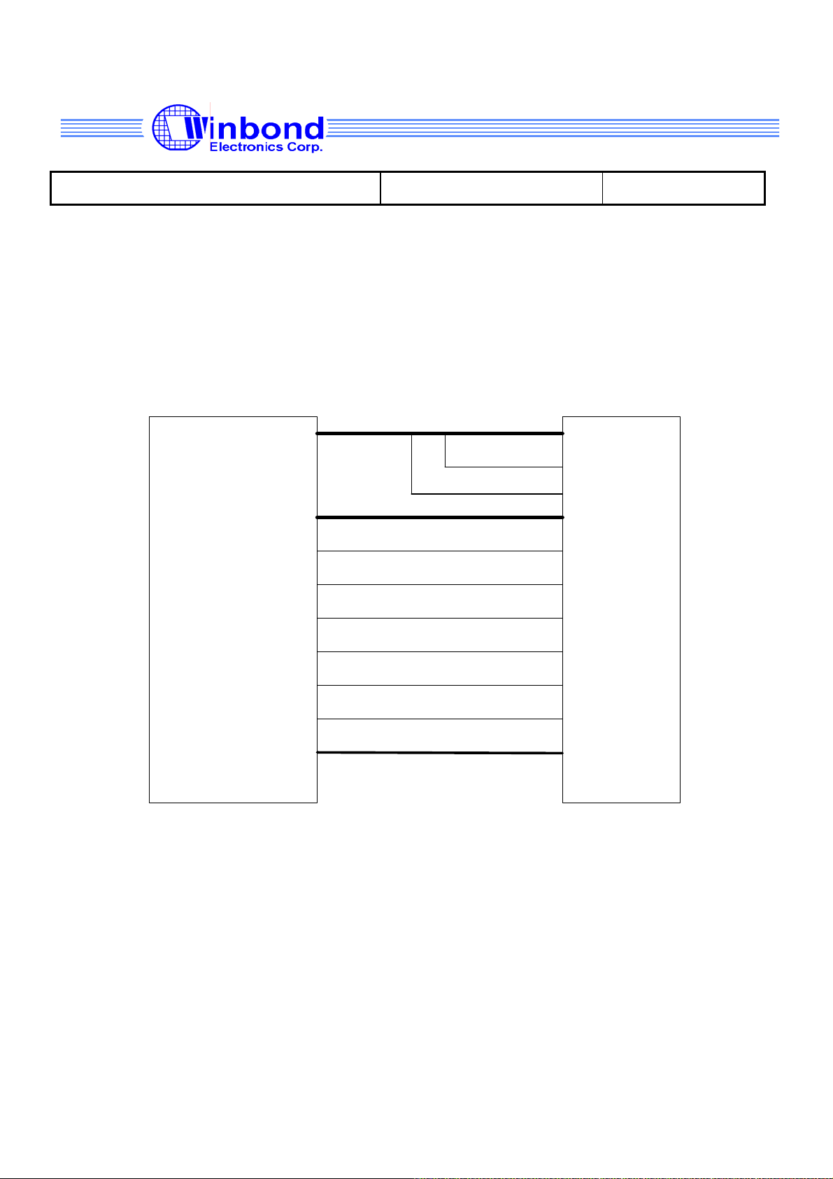
2.4.5 A system memory initialization example flow chart
Figure 2-2 System Memory Map Setting Flow
The above information is the exclusive intellectual property of Winbond Electronics and shall not be disclosed,
distributed or reproduced without permission from Winbond.
Table No.: 1200-0003-07-A
Page 31

NO: W90P710 Programming Guide VERSION: 2.1 PAGE: 31
Reset Go
Does the system have
been initialized?
Calculating the correct instruction fetch address
after remapping boot FLASH/ROM base addre ss
Calculating the correct instruction fetch address
after remapping boot FLASH/ROM base addre ss
Set the EBICON, ROMCON, SDCONF0,
SDCONF1, SDTIME0, and SDTIME1 at the sa me
time by store multiple instr u cti on.
Branch to the correct instructi on fet ch address
calculated before.
Execute boot software
Example:
EBICON = 0x000509C 1
ROMCON = 0xFFA00724 (base=0x7FD00000 size=256KB)
SDCONF0 = 0x000010ED (base=0x00000000 size=32MB )
SDCONF0 = 0x040010ED (base=0x02000000 size=32MB )
SDTIME0 = 0x000007FF
SDTIME0 = 0x000007FF
Boot FLASH/ROM 256KB
Before Initialization
0x7FFFFFFF
0x00040000
0x00000000
Boot FLASH/ROM 256KB
SDRAM BANK 1
SDRAM BANK 0
After Initialization
0x7FFFFFFF
0x7FD000000
0x04000000
0x02000000
0x00000000
Figure 2-4 is the boot flow of Boot Monitor with remapping. The flow chart shows that most of the
EBI control registers, EBICON, ROMCON, SDCONF, SDTIME should beware initialized as soon as
possible immediately after reset. Each value of these control register must be known before these
registers were configured. Because on doing of remapping, the control registers should be set by store
multiple instructions (STMIA). The store multiple instructions guarantee to complete the memory
initialization before next instruction execution. The system memory maps before initialization and after
initialization are shown as above, too. After system reset, the system can access the 256KB boot
FLASH/ROM. After the system initialization the memory map becomes the After Initialization of Figure
2-4.
The above information is the exclusive intellectual property of Winbond Electronics and shall not be disclosed,
distributed or reproduced without permission from Winbond.
Table No.: 1200-0003-07-A
Page 32

NO: W90P710 Programming Guide VERSION: 2.1 PAGE: 32
2.4.6 REMAPPING
RAM is normally with faster access speed and wider than ROM. For this reason, it is better to store
for the vector table and interrupt handlers if the memory on system address at 0x0 is of RAM. However,
if RAM is located at address 0x0 on power-up, there is not a valid instruction in the reset vector (0x0)
entry. Therefore, you must allow ROM to be located at 0x0 during normal execution. The changeover
remapping from the reset to the normal memory map is normally caused by writing to a memory-
mapped register.
In W90P710 the memory remapping can be achieved by setting EBI control registers. The following
example is a MACRO, which achieves performs the remapping when booting. The program flow of this
example is as Figure 2-4.
In general, the memory remapping only needs to be preformed once at reset. Thus the reset value
of SDCONF0 is used to check if the system has been initialized. If the system memory needs to do
remapping, the correct instructions to be fetched after remapping is important are critical. Therefore, the
MACRO will calculate the correct instruction fetch address after remapping. It does this by using labels
and program counter to know get the current execution position and execution position decided at link-
time. If the current execution position is different to from execution position decided at link-time, the
MACRO will calculate the correct instruction fetch address after remapping according to their address
relation. Finally, the value of PC will be update immediately after remapping. Because the memory
bases can be controlled by registers, what we called remapping means setting the EBI control registers.
The configuration values are predefined as rEBICON, rROMCON, rSDCONF0, rSDCONF1, rSDTIME0,
rSDTIME1, and are stored to relative control registers by store multiple instruction (STMIA). The source
code is listed as follows:
The above information is the exclusive intellectual property of Winbond Electronics and shall not be disclosed,
distributed or reproduced without permission from Winbond.
Table No.: 1200-0003-07-A
Page 33

NO: W90P710 Programming Guide VERSION: 2.1 PAGE: 33
; -----------------------------------------------------------------; UNMAPROM
; -------; Provide code to deal with mapping the reset ROM away from zero
MACRO
$label UNMAPROM $w1,$w2
; This macro needs to test if the system has already been init ialized
; The reset value of SDCONF0 is used to check if the system has been initialized
LDR $w1, =SDCONF0 ;SDCONF0=0xFFF01008
LDR $w1, [$w1]
LDR $w2, =0x800
CMP $w1, $w2
BNE %FT0
; Set mode to SVC, interrupts disabled (just paranoid)
MRS $w1, cpsr
BIC $w1, $w1, #0x1F
ORR $w1, $w1, #0xD3
MSR cpsr_fc, $w1
; Configure the EBI controller to remap the flash
; The EBI Control Registers must be set using store multiples
; Set up a stack in internal SRAM to preserve the original register contents
; Disable Cache and use the on-chip SRAM to be stack
LDR $w1, =CAHCNF ; CAHCNF=0xFFF02000
LDR $w2, =0x0 ; SetValue = 0x0
STR $w2, [$w1] ; Cache,WB disable
; W90P710 _SRAM_BASE = 0x7FE00000
; W90P710 _SRAM_SIZe = 10 Kbytes
MOV $w1, sp
LDR sp, =(W90P710 _SRAM_BASE+W90P710 _SRAM_SIZE)
STR $w1, [sp, #-4]! ; preserve previous sp on new stack
STMFD sp!, {r0 - r12,lr}
; The labels “$label.temp” and “$label.EndSysMapJump are absolute addresses
; calculated by linker according to the RO base.
LDR r2, =$label.temp
; The value of current pc is the run-time address of “$label.temp”
MOV r1, pc
LDR r3, =$label.EndSysMapJump
The above information is the exclusive intellectual property of Winbond Electronics and shall not be disclosed,
distributed or reproduced without permission from Winbond.
Table No.: 1200-0003-07-A
Page 34

NO: W90P710 Programming Guide VERSION: 2.1 PAGE: 34
$label.temp
MOV lr, #0
; If r2 > r1, the system needs to remapping.
; The RO_base is W90P710 _FLASH_BASE at link-time, thus we needs it to
; Calculate the correct instruction fetch address after remapping
CMP r2, r1
LDRGT lr, =W90P710 _FLASH_BASE
; Calculate the actual fetch address where is the location of
; the label “$label.EndSysMapJump” after remapping
SUB r3, r3, r2
ADD r1, r1, r3
ADD lr, lr, r1
; Load in the target values into the control registers
ADRL r0, $label.SystemInitData
LDMIA r0, {r1-r6}
LDR r0, =EBICON
; Now run critical jump code
STMIA r0, {r1-r6}
MOV pc, lr
$label.EndSysMapJump
; Now running from new PROM location, since code no long er exists in low memory
; Restore registers
LDMFD sp!, {r0 - r12,lr}
LDR $w1, [sp], #4
MOV sp, $w1
B %FT0
$label.SystemInitData
DCD rEBICON ; REFEN=1,REFMOD=0,CL KE N=1,R EFR AT=0 x13 8,WAI TV T=0
DCD rROMCON ; base=W90P710 _ FLA SH_B ASE ,siz e=2 56KB,B T SIZE=3 2bi t ,
; tPA=8MCLK,tACC=8MCLK
DCD rSDCONF0; base=0x0,size= 32M B,MR SET =1,AU TO PR=1,L A TENCY= 3MC L K,
; LENGTH=1Byte,COMPBK=2bank, DBW D=32 bit ,COLU M= 8bit
DCD rSDCONF1; base=0x2000000,size=32MB,MRSET=1,AUTO PR=1 ,LA TENC Y=3 MCLK,
; LENGTH=1Byte,COMPBK=2bank, DBW D=32 bit ,COLU M= 8bit
DCD rSDTIME0 ; tRCD=8MCLK,tRDL=4MCLK,t RP=8M CLK,tRAS =8MC LK
DCD rSDTIME1 ; tRCD=8MCLK,tRDL=4MCLK,t RP=8M CLK,tRAS =8MC LK
ALIGN
0
MEND
The above information is the exclusive intellectual property of Winbond Electronics and shall not be disclosed,
distributed or reproduced without permission from Winbond.
Table No.: 1200-0003-07-A
Page 35

NO: W90P710 Programming Guide VERSION: 2.1 PAGE: 35
3 Cache Controller
3.1 Overview
The W90P710 incorporates a 4KB Instruction cache, a 4KB Data cache, and 8 words write buffer
to improve the system performance. The caches consist of high-speed SRAM that provides quicker
access time than external memory. If cache is enabled, the CPU tries to fetch instructions from I-
cache instead of external memory. Similarly, the CPU tries to read data from D-cache instead of
external memory. But note that the CPU will write data into both D-cache and write buffer (write-
through mode). If I-Cache / D-Cache were disabled, these cache memories can be treated as On-
Chip SRAM.
To raise the cache-hit ratio, these two caches are configured as two-way set associative
addressing. Both I-cache and D-Cache organization is 256 sets, two lines per set. Each cache has four
words cache line size. When a miss occurs, four words must be fetched consecutively from external
memory. The replacement algorithm is a LRU (Least Recently Used).
The above information is the exclusive intellectual property of Winbond Electronics and shall not be disclosed,
distributed or reproduced without permission from Winbond.
Table No.: 1200-0003-07-A
Page 36

NO: W90P710 Programming Guide VERSION: 2.1 PAGE: 36
3.2 Block Diagram
Figure 3-1 Instruction Cac h e Organization Block Diagram
0123410113031
Tag(20)
WSINDEX(7)
xx
Non-cacheable
Control bit
LV Way1 Tag0
LV
LV
W3 W2 W1 W0
W3 W2 W1 W0
W3 W2 W1 W0
Way1 Tag1
Way1 Tag127
4 words cache line
:
:
:
:
Way Select
:
:
Way1
20-bit
:
:
32-bit
Word select
20-bit
VLWay0 Tag0
Way0 Tag1
VL
:
:
Way0 Tag127
VL
Way0
4 words cache line
W3 W2 W1 W0
W3 W2 W1 W0
:
:
:
:
:
:
:
:
W3 W2 W1 W0
32-bit
:
:
Set0
Set1
:
:
Set127
Set0
Set1
:
:
Set127
7-bit
7-bit
Bits
32-bit
The above information is the exclusive intellectual property of Winbond Electronics and shall not be disclosed,
distributed or reproduced without permission from Winbond.
Table No.: 1200-0003-07-A
Page 37

NO: W90P710 Programming Guide VERSION: 2.1 PAGE: 37
Figure 3-2 Data Cache Organization Block Diagram
Tag(20)
WSINDEX(7)
0123410113031
xx
Non-cacheable
Control bit
LV Way1 Tag0
LV
LV
4 words cache line
W3 W2 W1 W0
W3 W2 W1 W0
:
:
W3 W2 W1 W0
20-bit
Way1 Tag1
:
:
Way1 Tag127
Way1
:
:
:
:
32-bit
Word select
20-bit
VLWay0 Tag0
Way0 Tag1
VL
:
:
Way0 Tag127
VL
Way0
4 words cache line
W3 W2 W1 W0
W3 W2 W1 W0
:
:
:
:
W3 W2 W1 W0
32-bit
:
:
:
:
:
:
Set0
Set1
:
:
Set127
Set0
Set1
:
:
Set127
7-bit
7-bit
Bits
Way Select
32-bit
The above information is the exclusive intellectual property of Winbond Electronics and shall not be disclosed,
distributed or reproduced without permission from Winbond.
Table No.: 1200-0003-07-A
Page 38

NO: W90P710 Programming Guide VERSION: 2.1 PAGE: 38
3.3 Registers
R : read only, W : write only, R/W : both read and write, C : Only value 0 can be written
Register Address R/W Description Reset Value
CAHCNF
0xFFF0.2000
R/W Cache configuration register 0x0000.0000
CAHCON 0xFFF0.2004 R/W Cache control register 0x0000.0000
CAHADR 0xFFF0.2008 R/W Cache address register 0x0000.0000
3.4 Functional Descriptions
3.4.1 On-Chip RAM
If I-Cache or D-Cache is disabled, it can be used as On-Chip SRAM. The size of On-Chip RAM
depends on the I-Cache and D-Cache enable bits ICAEN, DCAEN in Cache Configuration Register
(CAHCNF). The details listed in Table 3-1.
Table 3-1 The size and start address of On-Chip RAM
ICAEN DCAEN On-Chip RAM
Size Start Address
0 0 8KB 0x7FE0.0000
0 1 4KB 0x7FE0.0000
1 0 4KB 0x7FE0.1000
1 1 Unavailable
The above information is the exclusive intellectual property of Winbond Electronics and shall not be disclosed,
distributed or reproduced without permission from Winbond.
Table No.: 1200-0003-07-A
Page 39

NO: W90P710 Programming Guide VERSION: 2.1 PAGE: 39
3.4.2 Non-Cacheable Area
The cache affects the first 2GB system memory. Sometimes it is necessary to define non-
cacheable areas when the consistency of data stored in memory and the cache can’t be ensured. To
support this feature, the W90P710 provides a non-cacheable area control bit in the address field, A
[31]. If A [31] in the ROM/FLASH, SDRAM, or external I/O bank’s access address is “0”, then the
accessed data is cacheable. If the A [31] value is “1”, the accessed data is non-cacheable.
Cache Control Register
The Cache controller supports one Control register (CAHCON) to control cache flushing,
lock/unlock and drain write buffer. All the command set bits of CAHCON register are auto-clear bit. At
the end of execution, the command set bit will be cleared to “0” automatically. The detail description of
each bit filed can be found in W90P710 specification.
3.4.3 Cache Flushing
To prevent unpredictable error, it’s better to flush cache before enable it. Both I-Cache and D-
Cache can be entirely flushed in one operation, or be flushed one line at a time. The bit FLHA and
FLHS of register CAHCON are used to flush entire cache and single line, respectively. Bit DCAH or
ICAH of register CAHCON is used to select D-Cache or I-Cache for the flush operation. The Cache
Address Register (CAHADR) must be set before flush a single cache line.
Due to W90P710 does not support external memory snooping; it is necessary to flush cache if the
force consistency of cache and memory is required. For example, The I-Cache should be flushed
after a self-modifying code is executed. Similarly, the D-Cache should be flushed before an external
device starts a DMA transfer with a cacheable memory region.
3.4.4 Cache Enable and Disable
After the cache was flushed, the cache can be enabled. Bit ICAEN and DCAEN of register CAHCNF
is used to enable D-Cache and I-Cache. The D-Cache and I-Cache can be enabled individually, or
The above information is the exclusive intellectual property of Winbond Electronics and shall not be disclosed,
distributed or reproduced without permission from Winbond.
Table No.: 1200-0003-07-A
Page 40

NO: W90P710 Programming Guide VERSION: 2.1 PAGE: 40
enabled at the same time. The write buffer can be enabled by setting the WRBEN. Most of the time,
ICAEN, DCAEN and WRBEN are enabled at the same time.
3.4.5 Cache Load and Lock
The W90P710 cache controller supports a cache-locking feature that locks critical sections of
code or data into I-Cache or D-Cache. This guarantees the quick access to these critical sections.
Lockdown operation can be performed with a granularity of one cache line (4 words). The smallest
size, which can be locked down, is 4 words. After a line is locked, it operates as a regular instruction
SRAM. Locked lines don’t be replaced either cache misses or flush per line command. Figure 3-5
shows the steps for locking instructions or data.
Figure 3-3 Cache Load and Lock
Increased th e ad dress
by 16
No
start
Set CAHADR
Set CAHCON
Desired data are all
locke d ?
Yes
end
Write the start add ress o f the d a ta
to be locked into CAHADR
register
1. Set LDLK.
2. Set ICAH for I-cache, DCAH
for D-cache
There are some limitations during the locking cache line into the I-Cache or D-Cache.
The above information is the exclusive intellectual property of Winbond Electronics and shall not be disclosed,
distributed or reproduced without permission from Winbond.
Table No.: 1200-0003-07-A
Page 41

NO: W90P710 Programming Guide VERSION: 2.1 PAGE: 41
z The code that executes load and lock operation should be held in a non-cacheable area of
memory.
z The cache should be enabled and interrupts should be disabled.
z Flushed the cache before execute load and lock to ensure that the data to be locked down is
not already in the cache.
3.4.6 Cache Unlock
The unlock operation is used to unlock previously locked cache lines. The cache controller
provides two unlock command, unlock line and unlock all.
The unlock line operation is performed on a cache line granularity. In case the line is found in the
cache, it is unlocked and starts to operate as a regular valid cache line. In case the line is not found in
the cache, no operation is done and the command terminates with no exception. To unlock one line,
write the address of the line to be unlocked into the CAHADR Register, and then set the ULKS and
ICAH bits in the CAHCON register for I-cache or set the ULKS and DCAH bits for D-cache.
The unlock all operation is performed on all cache lines of I-Cache or D-Cache. In case a line is
locked, it is unlocked and starts to operate as regular valid cache line. In case a line is not locked or if
it is invalid, no operation is performed. To unlock the whole instruction cache, set the ULKA and ICAH
bits. To unlock the whole data cache, set the ULKA and DCAH bits.
The above information is the exclusive intellectual property of Winbond Electronics and shall not be disclosed,
distributed or reproduced without permission from Winbond.
Table No.: 1200-0003-07-A
Page 42

NO: W90P710 Programming Guide VERSION: 2.1 PAGE: 42
4 EMC (Ethernet MAC Controller)
4.1 Overview
The W90P710 provides a Ethernet MAC Controller (EMC) for WAN/LAN application. This EMC
has its DMA controller, transmit FIFO, and receive FIFO.
The Ethernet MAC controller consists of IEEE 802.3/Ethernet protocol engine with internal CAM
function for Ethernet MAC address recognition, Transmit-FIFO, Receive-FIFO, TX/RX state machine
controller and status controller. The EMC only supports RMII (Reduced MII) interface to connect
with PHY operating on 50MHz REF_CLK.
Features :
• Supports IEEE Std. 802.3 CSMA/CD protocol.
• Supports both half and full duplex for 10M/100M bps operation.
• Supports RMII interface.
• Supports MII Management function.
• Supports pause and remote pause function for flow control.
• Supports long frame (more than 1518 bytes) and short frame (less than 64 bytes) reception.
• Supports 16 entries CAM function for Ethernet MAC address recognition.
• Supports internal loop back mode for diagnostic.
• Supports 256 bytes embedded transmit and receive FIFO.
• Supports DMA function.
The above information is the exclusive intellectual property of Winbond Electronics and shall not be disclosed,
distributed or reproduced without permission from Winbond.
Table No.: 1200-0003-07-A
Page 43

NO: W90P710 Programming Guide VERSION: 2.1 PAGE: 43
4.2 Block Diagram
Figure 4-1 EMC Block Diagram
AHB Bus Interfac e
HCLK
Domain
RxFIFO
RxDMA
State Mach ine
RxFIFO
Control
AHB Bus Master
Arbiter
Flow Control
TxDMA
State Machine
TxFIFO
Control
AHB Bus
Slave
Register
Files
TxFIFO
MAC
Address
Register
MDC
Domain
MII Management
State Machine
MDCMDIO
TX_CLK
Domain
CSMA/CD
(RxMAC, TxMAC)
RMII2MII
RMII Interface
Station Management Interface
The above information is the exclusive intellectual property of Winbond Electronics and shall not be disclosed,
distributed or reproduced without permission from Winbond.
Table No.: 1200-0003-07-A
Page 44

NO: W90P710 Programming Guide VERSION: 2.1 PAGE: 44
4.3 Registers
4.3.1 EMC Control registers
Register Address R/W Description Reset Value
CAMCMR
CAMEN
CAM0M
CAM0L
CAM1M
CAM1L
CAM2M
CAM2L
CAM3M
CAM3L
CAM4M
CAM4L
CAM5M
CAM5L
CAM6M
CAM6L
CAM7M 0xFFF0.3040 R/W CAM7 Most Significant Word Register 0x0000.0000
CAM7L
CAM8M
CAM8L
CAM9M
CAM9L
CAM10M
CAM10L
CAM11M
CAM11L
CAM12M
CAM12L
CAM13M
CAM13L
CAM14M
CAM14L
CAM15M
CAM15L
TXDLSA
RXDLSA
MCMDR
The above information is the exclusive intellectual property of Winbond Electronics and shall not be disclosed,
distributed or reproduced without permission from Winbond.
Table No.: 1200-0003-07-A
0xFFF0.3000 R/W CAM Command Register 0x0000.0000
0xFFF0.3004 R/W CAM Enable Register 0x0000.0000
0xFFF0.3008 R/W CAM0 Most Significant Word Register 0x0000.0000
0xFFF0.300C R/W CAM0 Least Significant Word Register 0x0000.0000
0xFFF0.3010 R/W CAM1 Most Significant Word Register 0x0000.0000
0xFFF0.3014 R/W CAM1 Least Significant Word Register 0x0000.0000
0xFFF0.3018 R/W CAM2 Most Significant Word Register 0x0000.0000
0xFFF0.301C R/W CAM2 Least Significant Word Register 0x0000.0000
0xFFF0.3020 R/W CAM3 Most Significant Word Register 0x0000.0000
0xFFF0.3024 R/W CAM3 Least Significant Word Register 0x0000.0000
0xFFF0.3028 R/W CAM4 Most Significant Word Register 0x0000.0000
0xFFF0.302C R/W CAM4 Least Significant Word Register 0x0000.0000
0xFFF0.3030 R/W CAM5 Most Significant Word Register 0x0000.0000
0xFFF0.3034 R/W CAM5 Least Significant Word Register 0x0000.0000
0xFFF0.3038 R/W CAM6 Most Significant Word Register 0x0000.0000
0xFFF0.303C R/W CAM6 Least Significant Word Register 0x0000.0000
0xFFF0.3044 R/W CAM7 Least Significant Word Register 0x0000.0000
0xFFF0.3048 R/W CAM8 Most Significant Word Register 0x0000.0000
0xFFF0.304C R/W CAM8 Least Significant Word Register 0x0000.0000
0xFFF0.3050 R/W CAM9 Most Significant Word Register 0x0000.0000
0xFFF0.3054 R/W CAM9 Least Significant Word Register 0x0000.0000
0xFFF0.3058 R/W CAM10 Most Significant Word Register 0x0000.0000
0xFFF0.305C R/W CAM10 Least Significant Word Register 0x0000.0000
0xFFF0.3060 R/W CAM11 Most Significant Word Register 0x0000.0000
0xFFF0.3064 R/W CAM11 Least Significant Word Register 0x0000.0000
0xFFF0.3068 R/W CAM12 Most Significant Word Register 0x0000.0000
0xFFF0.306C R/W CAM12 Least Significant Word Register 0x0000.0000
0xFFF0.3070 R/W CAM13 Most Significant Word Register 0x0000.0000
0xFFF0.3074 R/W CAM13 Least Significant Word Register 0x0000.0000
0xFFF0.3078 R/W CAM14 Most Significant Word Register 0x0000.0000
0xFFF0.307C R/W CAM14 Least Significant Word Register 0x0000.0000
0xFFF0.3080 R/W CAM15 Most Significant Word Register 0x0000.0000
0xFFF0.3084 R/W CAM15 Least Significant Word Register 0x0000.0000
0xFFF0.3088 R/W Transmit Descriptor Link List Start Address
Register
0xFFF0.308C R/W Receive Descriptor Link List Start Address
Register
0xFFF0.3090 R/W MAC Command Register 0x0000.0000
0xFFFF.FFFC
0xFFFF.FFFC
Page 45

NO: W90P710 Programming Guide VERSION: 2.1 PAGE: 45
MIID
MIIDA
FFTCR
TSDR
RSDR
DMARFC
MIEN
0xFFF0.3094 R/W MII Management Data Register 0x0000.0000
0xFFF0.3098 R/W MII Management Control and Address
Register
0xFFF0.309C R/W FIFO Threshold Control Register 0x0000.0101
0xFFF0.30A0 W Transmit Start Demand Register Undefined
0xFFF0.30A4 W Receive Start Demand Register Undefined
0xFFF0.30A8 R/W Maximum Receive Frame Control Register 0x0000.0800
0xFFF0.30AC R/W MAC Interrupt Enable Register 0x0000.0000
0x0090.0000
4.3.2 EMC Status Registers
Register Address R/W Description Reset Value
MISTA
MGSTA
MPCNT
MRPC
MRPCC
MREPC
DMARFS
CTXDSA
CTXBSA
CRXDSA
CRXBSA
0xFFF0.30B0 R/W MAC Interrupt Status Register 0x0000.0000
0xFFF0.30B4 R/W MAC General Status Register 0x0000.0000
0xFFF0.30B8 R/W Missed Packet Count Register 0x0000.7FFF
0xFFF0.30BC R MAC Receive Pause Count Register 0x0000.0000
0xFFF0.30C0 R MAC Receive Pause Current Count Register 0x0000.0000
0xFFF0.30C4 R MAC Remote Pause Count Register 0x0000.0000
0xFFF0.30C8 R/W DMA Receive Frame Status Register 0x0000.0000
0xFFF0.30CC R Current Transmit Descriptor Start Address
Register
0xFFF0.30D0 R Current Transmit Buffer Start Address Register 0x0000.0000
0xFFF0.30D4 R Current Receive Descriptor Start Address
Register
0xFFF0.30D8 R Current Receive Buffer Start Address Register 0x0000.0000
0x0000.0000
0x0000.0000
4.4 Functional Descriptions
4.4.1 Initialize Rx Buffer Descriptors
(1) Allocate memory for Rx descriptors.
(2) Write start address of (1) to RXDLSA register and let Rx software pointer point to this
address.
(3) Set ownership bits of each descriptor to DMA.
(4) Allocate memory as data buffer and write the address to data buffer start address field of Rx
descriptor.
(5) Set start address of next descriptor, this field of the last descriptor should set to the address
of the first descriptor.
The above information is the exclusive intellectual property of Winbond Electronics and shall not be disclosed,
distributed or reproduced without permission from Winbond.
Table No.: 1200-0003-07-A
Page 46

NO: W90P710 Programming Guide VERSION: 2.1 PAGE: 46
(6) The start address of descriptor and data buffer are suggested to be aligned to 16 bytes
address boundary.
Figure 4-2 lists the Rx Descriptor initialization flow.
The above information is the exclusive intellectual property of Winbond Electronics and shall not be disclosed,
distributed or reproduced without permission from Winbond.
Table No.: 1200-0003-07-A
Page 47

NO: W90P710 Programming Guide VERSION: 2.1 PAGE: 47
Figure 4-2 Rx Descriptor Initialization
Start
Allocate memory (16 bytes boundary) for Rx
Buffer Descriptors
Write the start address of allocated Rx Buffer
Descriptors to RXDLS A, also initialized Rx
software pointer
Set ownership bits of each descriptor to DMA
Allocate memory for Rx data buffers( 4-Bytes
boundary), and write the address of data buffer to
Data Buffer Start Address field of each Rx Buffer
Descriptor
Get the start address of next descriptor, set it to
Start Address of Next Descriptor field of current
descriptor until the last one, the last descriptor
should link to the first one to form a descriptor ring
End
The above information is the exclusive intellectual property of Winbond Electronics and shall not be disclosed,
distributed or reproduced without permission from Winbond.
Table No.: 1200-0003-07-A
Page 48

NO: W90P710 Programming Guide VERSION: 2.1 PAGE: 48
4.4.2 Initialize Tx Buffer Descriptors
(1) Allocate memory for Tx descriptors.
(2) Write start address of (1) to TXDLSA register and let Tx software pointer point to this
address.
(3) Set ownership bits of each descriptor to CPU.
(4) Allocate memory to save frame data and write the address to data buffer start address field of
Tx descriptor.
(5) Set start address of next descriptor, this field of the last descriptor should set to the address
of the first descriptor.
(6) Set I,C,P bits of each descriptor(The bits can also be set before transmitting packets).
(7) The start address of descriptor and data buffer are suggested to be 16 bytes alignment.
Figure 4-3 lists the Tx Descriptor initialization flow.
The above information is the exclusive intellectual property of Winbond Electronics and shall not be disclosed,
distributed or reproduced without permission from Winbond.
Table No.: 1200-0003-07-A
Page 49

NO: W90P710 Programming Guide VERSION: 2.1 PAGE: 49
Figure 4-3 Tx Descriptor Initialization
Start
Allocate memory (16 bytes boundary) for Tx
Buffer Descriptors
Write the start address of allocated Tx Buffer
Descriptors to TXDLSA, also initialized Tx
software pointer
Set ownership bits of each descriptor to CPU
Allocate memory for Tx data buffers( 4-Bytes
boundary), and write the address of data buffer to
Data Buffer Start Address field of each Tx Buffer
Descriptor
Get the start address of next descriptor, set it to
Start Address of Next Descriptor field of current
descriptor until the last one, the last descriptor
should link to the first one to form a descriptor ring
Set I, C, P bits of each descriptor(These bits also
can be set before transmit packets)
End
The above information is the exclusive intellectual property of Winbond Electronics and shall not be disclosed,
distributed or reproduced without permission from Winbond.
Table No.: 1200-0003-07-A
Page 50

NO: W90P710 Programming Guide VERSION: 2.1 PAGE: 50
4.4.3 MII
4.4.3.1 MII Management Function Configure Sequence
Read Write
1. Set appropriate MDCCR.
2. Set PHYAD and PHYRAD.
3. Set Write to 1’b0
4. Set bit BUSY to 1’b1 to send a MII
management frame out.
5. Wait BUSY to become 1’b0.
6. Read data from MIID register.
7. Finish the read command.
4.4.3.2 PHY Registers Programming
1. Write data to MIID register
2. Set appropriate MDCCR.
3. Set PHYAD and PHYRAD.
4. Set Write to 1’b1
5. Set bit BUSY to 1’b1 to send a MII
management frame out.
6. Wait BUSY to become 1’b0.
7. Finish the write command.
Control Register(0x00).
Bit Function
15 Reset
14 Loopback
13 Speed (1=100MB, 0=10MB)
12 Auto-negotiation Enable
11 Power-Down
10 Isolate
09 Restart auto-negotiation
08 Duplex Mode (1=Full, 0=Half)
07 Collision test
Status Register #1(0x01)
Bit Function
15 100BASE-T4 capable
14 100BASE-TX full duplex capable
13 100BASE-TX half duplex capable
12 10BASE-T full duplex capable
The above information is the exclusive intellectual property of Winbond Electronics and shall not be disclosed,
distributed or reproduced without permission from Winbond.
Table No.: 1200-0003-07-A
Page 51

NO: W90P710 Programming Guide VERSION: 2.1 PAGE: 51
11 10BASE-T half duplex capable
06 Accept management frames with
preamble suppressed
05 Auto-negotiation complete
04 Remote fault
03 Auto-negotiation capable
02 Link status(1=Up, 0=Down)
01 Jabber condition detected
00 Extended register capable
Auto-negotiation Advertisement Register(0x04)
Protocol selection (00001-IEEE802.3)
Bit Function
15 Next page available
13 Remote fault
10 Flow control support
09 100BASE-T4 support
08 100BASE-TX full duplex support
07 100BASE-TX half duplex support
06 10BASE-T full duplex support
05 10BASE-T half duplex support
04 ~ 00 Protocol selection (00001-IEEE802.3)
Status Register #2(0x11)
Current speed(10M/100M) and operation(full/half duplex) can read from this register, the
exact bit position should refer to the PHY datasheet.
Example for auto-negotiation
(1) Set “auto-negotiation enable” and “restart auto-negotiation”(bits 12 and 9) of control
register
(2) Wait auto-negotiation complete by reading “auto-negotiation complete”(bit 5) of status
register #1 until it is set
(3) Read status register #2 to get speed and operation mode that is the result of auto-
negotiation.
(4) Set speed and operation mode of MAC
The above information is the exclusive intellectual property of Winbond Electronics and shall not be disclosed,
distributed or reproduced without permission from Winbond.
Table No.: 1200-0003-07-A
Page 52

NO: W90P710 Programming Guide VERSION: 2.1 PAGE: 52
4.4.4 Control Frames
4.4.4.1 Receive Control Pause Frame
1. sdklfn
2.
3. Set ACP bit in MCMDR
4. The Multicast address “01-80-c2-00-00-01” should fill to CAM if AMP not set
5. Set EnCFR in MIEN if want to handle control frame receive interrupt
4.4.4.2 Send Control Pause Frame
1. Fill the destination MAC address to CAM#13
2. Fill the source MAC address to CAM#14
3. Fill length/type(0x8808), opcode(0x0001) and operand(timeslot) to CAM#15
4. Set SDPZ bit in MCMDR
5. Wait control pause frame transmission complete by reading SDPZ bit until it is 0
4.4.5 Packet Processing
4.4.5.1 Packet Transmission
(1) Get Tx buffer descriptor from Tx software pointer.
(2) Check ownership of (1), do nothing if ownership is DMA.
(3) Allocate data buffer and set start address to data buffer starting address field of (1).
(4) Copy packet data to data buffer.
(5) Set I,C,P bits if need.
(6) Set packet length to frame length field of (1).
(7) Set ownership to DMA.
(8) Set TXON bit of MCMDR register if it is not set.
(9) Write TSDR register.
The above information is the exclusive intellectual property of Winbond Electronics and shall not be disclosed,
distributed or reproduced without permission from Winbond.
Table No.: 1200-0003-07-A
Page 53

NO: W90P710 Programming Guide VERSION: 2.1 PAGE: 53
Figure 4-4 Packet Transmission Flow
Ready to Transmit Packet
Get a Tx Buffer Descriptor from Tx Software Buffer
Descriptor Pointer
Check ownership bits, CPU ?
Y
Allocate data buffer for storing transmitting packets, set
the start address of data buffer to Data Buffer Starting
Address field of buffer descriptor
Copy Transmitting packet data to allocated buffer
Set I, C, P bits if needed
Set length of the packet to Frame Length field of
descriptor
Set ownership bits to DMA
N
Run out of Descriptors,
Exception Handling
Set TXON bit of MCMDR register if it didn't be set
Write TSDR register
MAC Processing
The above information is the exclusive intellectual property of Winbond Electronics and shall not be disclosed,
distributed or reproduced without permission from Winbond.
Table No.: 1200-0003-07-A
Page 54

NO: W90P710 Programming Guide VERSION: 2.1 PAGE: 54
4.4.5.2 Tx Interrupt Service Routine
(1) Get and check status in MISTA.
(2) Set software reset bit in FIFOTHD and re-initialize MAC if bus error occur. Do the following
step if no error occur.
(3) Get status from the descriptor of Tx software pointer. Do the following steps if TXCP bit is set.
(4) Free data buffer allocated to this descriptor.
(5) Set the next descriptor to Tx software pointer.
(6) Transmit the next packet if there is packet available in device queue.
The above information is the exclusive intellectual property of Winbond Electronics and shall not be disclosed,
distributed or reproduced without permission from Winbond.
Table No.: 1200-0003-07-A
Page 55

NO: W90P710 Programming Guide VERSION: 2.1 PAGE: 55
Figure 4-5 Tx Interrup t Service Routine Flow
Enter Tx ISR
Check status of MISTA
Set Software Reset
Bus Error ?
N
Get Status from Tx Buffer
Descriptor pointed by Tx S/W
pointer
Y
bit in FIFOTHD to
reset MAC
TXCP bit set ?
Y
Free data buffer allocated for
the transmitted packet
Update the Tx S/W descriptor
pointer to next Tx Buffer
Descriptor
Transmit the next packet if
there is any packet available in
the device queue
End of Tx ISR
N
Error Handling for
other interrupt cause.
The above information is the exclusive intellectual property of Winbond Electronics and shall not be disclosed,
distributed or reproduced without permission from Winbond.
Table No.: 1200-0003-07-A
Page 56

NO: W90P710 Programming Guide VERSION: 2.1 PAGE: 56
4.4.5.3 Rx Interrupt Service Routine
(1) Get and check status in MISTA.
(2) Set software reset bit in FIFOTHD and re-initialize MAC if bus error occur. Do the following
step if no error occur.
(3) Get ownership from the descriptor of Rx software pointer. Do the following step if ownership is
CPU.
(4) Get status from the descriptor of Rx software pointer. Do the following steps if RXGD bit is set.
(5) Change ownership to DMA.
(6) Set the next descriptor to Rx software pointer.
(7) Re-start from step (3) if descriptor of Rx software pointer is not the same as the one of
CRXDSA register.
(8) Write RSDR register.
The above information is the exclusive intellectual property of Winbond Electronics and shall not be disclosed,
distributed or reproduced without permission from Winbond.
Table No.: 1200-0003-07-A
Page 57

NO: W90P710 Programming Guide VERSION: 2.1 PAGE: 57
Figure 4-6 Rx Interrupt Service Routine
Check MISTA
Bus Error ?
Check the ownership bits on the Rx Buffer Descriptor pointer by S/W pointer.
CPU ?
Y
Get Rx Status from the status field of Rx Buffer Descriptor.
N
Copy the received data to buffer
provided by upper protocol layer
Change ownership bits to DMA
Update the Rx S/W descriptor pointer to next descriptor
RXGD ?
Y
Y
Run out of Rx Buffer Descriptor,
N
Error Handling for Receive Frame
N
MAC Software Reset
by FIFOTHD
Exception Hadling
Error
Rx S/W Descriptor pointer the
same as CRXDSA
Y
Write RSDR
Exit Rx ISR
The above information is the exclusive intellectual property of Winbond Electronics and shall not be disclosed,
distributed or reproduced without permission from Winbond.
Table No.: 1200-0003-07-A
Page 58

NO: W90P710 Programming Guide VERSION: 2.1 PAGE: 58
5 GDMA
5.1 Overview
The W90P710 GDMA controller provides a data transfer mechanism without the need of CPU
intervention. It can move data between two memory regions, or between memory and external
devices. The GDMA has two independent channels that support single and block mode transfer.
When GDMA is programmed to single mode, it requires a request (nXDREQ) for each data transfer
that may be one byte, one half-word or one word. When GDMA is programmed to block mode, a
single GDMA request will make all of the data to be transferred.
The data transfer can be started after write the control register or receive an external DMA
request (nXDREQ). The GDMA will try to finish the data transfer according to the transfer mode,
source address, destination address and transfer count. The device driver can recognize the
completion of a GDMA operation by polling control register or when it receives a GDMA interrupt.
The W90P710 GDMA controller implements many flexible features to support the data transfers.
It can increment or decrement source or destination address during the data transfer, and conduct
with 8-bit (byte), 16-bit (half-word), or 32-bit (word) size data transfers. The source or destination
address of the GDMA can be fixed also. Furthermore, the GDMA supports 4-data burst mode to boost
performance and supports demand mode to speed up external GDMA operations.
The above information is the exclusive intellectual property of Winbond Electronics and shall not be disclosed,
distributed or reproduced without permission from Winbond.
Table No.: 1200-0003-07-A
Page 59

NO: W90P710 Programming Guide VERSION: 2.1 PAGE: 59
5.2 Block Diagram
Figure 5-1 GDMA Bloc k D ia g ra m
AHB Bus Interface
GDMA Channel 0
nDREQ
GDMA block
GDMA Channel 1
nDACK
nDREQ
SWREQ 0 SWREQ 1
nDACK
External
GDMA
Interface
nXDACK
nXDREQ
The above information is the exclusive intellectual property of Winbond Electronics and shall not be disclosed,
distributed or reproduced without permission from Winbond.
Table No.: 1200-0003-07-A
Page 60

NO: W90P710 Programming Guide VERSION: 2.1 PAGE: 60
5.3 Registers
R : read only, W : write only, R/W : both read and write, C : Only value 0 can be written
Register Address R/W Description Reset Value
GDMA_CTL0
GDMA_SRCB0
GDMA_DSTB0
GDMA_TCNT0
GDMA_CSRC0
GDMA_CDST0
GDMA_CTCNT0
GDMA_CTL1
GDMA_SRCB1
GDMA_DSTB1
GDMA_TCNT1
GDMA_CSRC1
GDMA_CDST1
GDMA_CTCNT1
0xFFF0.4000 R/W Channel 0 Control Register 0x0000.0000
0xFFF0.4004 R/W Channel 0 Source Base Address Register 0x0000.0000
0xFFF0.4008 R/W Channel 0 Destination Base Address Register 0x0000.0000
0xFFF0.400C R/W Channel 0 Transfer Count Register 0x0000.0000
0xFFF0.4010 R Channel 0 Current Source Address Register 0x0000.0000
0xFFF0.4014 R Channel 0 Current Destination Address Register 0x0000.0000
0xFFF0.4018 R Channel 0 Current Transfer Count Register 0x0000.0000
0xFFF0.4020 R/W Channel 1 Control Register 0x0000.0000
0xFFF0.4024 R/W Channel 1 Source Base Address Register 0x0000.0000
0xFFF0.4028 R/W Channel 1 Destination Base Address Register 0x0000.0000
0xFFF0.402C R/W Channel 1 Transfer Count Register 0x0000.0000
0xFFF0.4030 R Channel 1 Current Source Address Register 0x0000.0000
0xFFF0.4034 R Channel 1 Current Destination Address Register 0x0000.0000
0xFFF0.4038 R Channel 1 Current Transfer Count Register 0x0000.0000
5.4 Functional Descriptions
5.4.1 GDMA Configuration
Each GDMA channel has one control register, two base address registers and one transfer count
register. These registers should be correctly programmed before the data transfer starts. The most
important one is the control register (GDMA_CTL). It is used to control the transfer behavior of the
GDMA operation, such as the transfer mode, transfer count, transfer width and interrupt mask. Figure
5-2 lists the content of GDMA_CTL. The detail description of each bit-field can be found in W90P710
data sheet.
The above information is the exclusive intellectual property of Winbond Electronics and shall not be disclosed,
distributed or reproduced without permission from Winbond.
Table No.: 1200-0003-07-A
Page 61

NO: W90P710 Programming Guide VERSION: 2.1 PAGE: 61
Figure 5-2 The bit-fields of the GDMA control register.
31 30 29 28 27 26 25 24
RESERVED
23 22 21 20 19 18 17 16
RESERVED SABNDERR DABNDERR GDMAERR AUTOIEN TC BLOCK SOFTREQ
15 14 13 12 11 10 9 8
DM RESERVED TWS SBMS RESERVED BME SIEN
7 6 5 4 3 2 1 0
SAFIX DAFIX SADIR DADIR GDMAMS RESERVED GDMAEN
The source base address register (GDMA_SRCB) is used to set the base address of source data.
The destination base address register (GDMA_DSTB) is used to set the starting address where the
source data to be stored. The number of the GDMA transfer is set by programming the transfer count
register (GDMA_TCNT). The GDMA operation is continued until the transfer count register is counted
down to zero. Figure 5-3 shows the programming flow for GDMA operation.
The above information is the exclusive intellectual property of Winbond Electronics and shall not be disclosed,
distributed or reproduced without permission from Winbond.
Table No.: 1200-0003-07-A
Page 62

NO: W90P710 Programming Guide VERSION: 2.1 PAGE: 62
Figure 5-3 GDMA operations
Start
If the SOFTREQ was not self-clean in the
Clean co ntrol register
previo us G DMA t ra nsfer, it shou ld be clean ed
before next GDMA transfer req uest.
The mode, direction, fixing, bust,
bus lock, transfer width, block
mode, interrupt are set here.
5.4.2 Transfer Count
Set source add r ess
Set destination address
Set tra ns fe r c o un t
Set con trol r egist er
No
Transfer complete ?
Clear [TC]
Should be at the natu re boundar y of T WS
Should be at the na tur e b o un d a r y of TWS
24-bit (maximum is 16M-1), each count represents:
i. 8 bits w h en 8-bit transfer.
ii. 16 b its w h en 1 6-bit trans fer .
iii. 32 b its w h en 3 2 -b it tr ansfer.
iv. 8*4, 16*4, or 32*4 bits when burst mode enabled.
Yes
End
The value in register GDMA_TCNT is the transfer count, not the byte count. Normally, the
number of final transferred bytes is calculated by the following equation.
Transferred bytes = [GDMA_TCNT] * Transfer width /* burst mode is disabled */
For example, supposes that [GDMA_TCNT] = 16 and the transfer width is half-word (16-bit). The
number of transferred bytes should be 16 * 2 = 32. But if the burst mode is enabled, the above
equation will be changed as below.
The above information is the exclusive intellectual property of Winbond Electronics and shall not be disclosed,
distributed or reproduced without permission from Winbond.
Table No.: 1200-0003-07-A
Page 63

NO: W90P710 Programming Guide VERSION: 2.1 PAGE: 63
Transferred bytes = [GDMA_TCNT] * Transfer width * 4 /* burst mode is enabled */
In case of burst mode is enabled, the transferred bytes of the above example should be 16 * 2 * 4
= 128
5.4.3 Transfer Termination
When GDMA finishes the transfer, it will set the bit [TC] of register GDMA_CTRL and generate an
interrupt request if the interrupt is enabled. The device driver can either poll the bit [TC] or wait the
GDMA interrupt occurs to know the transfer is completed. Note that the device driver must clear bit
[TC] to clear this interrupt request to let the next GDMA operation to continue.
5.4.4 GDMA operation started by software
The GDMA can be configured as software mode to perform memory-to-memory transfer. In this
mode, the transfer operation starts as soon as the setting of the GDMA control registers are set, the
setting of source address, destination address, and transfer count should be programmed in
advanced. The programming method of software mode is listed below:
(1) Set the GDMA to software mode (GDMAMS=00b).
(2) Set the GDMA to Block Mode.
(3) After all configuration of the GDMA, set [SOFTREQ] = 1 and [GDMAEN] = 1 to start
the GDMA operation.
(4) Single mode is invalid.
(5) Demand mode is invalid.
In software mode, bit SOFTREQ and GDMAEN are self-cleared. The GDMA controller
automatically clears these 2 bits after transfer completed. However, GDMAEN won’t be self-clear if
AUTOIEN bit is set. Hence, the driver only needs to set bit SOFTREQ to start next data transfer. If the
GDMA didn’t complete this transfer, it will cause the GDMA transfer error bit to be set, and the
The above information is the exclusive intellectual property of Winbond Electronics and shall not be disclosed,
distributed or reproduced without permission from Winbond.
Table No.: 1200-0003-07-A
Page 64

NO: W90P710 Programming Guide VERSION: 2.1 PAGE: 64
SOFTREQ won’t be self-cleared. In this case, the SOFTREQ bit should be cleared before next
software GDMA request.
It should be note that the source and destination base address must be in the right alignment
according to its transfer width. For example, if the transfer width is 32-bit, the source and destination
base address should be word-alignment. If each one is not aligned, the GDMA will read from and
write to wrong addresses and the alignment error flags, SABNDERR and DABNDERR, will be set.
Figure 5-4 shows an example code for software GDMA transfer.
Figure 5-4 Software GDMA Transfer
#define BA SE0xc0000000
#define G D M A _SRCB0 (B A SE+0xFF04004)
#define G D M A _D ST B0 (B ASE +0xFF04008)
#define G D M A _TC NT0 (B A SE+0xFF0400C)
#define G D M A _C SRC 0 (B ASE +0xFF04010)
#define G D M A _C D ST0 (B ASE +0xFF04014)
#define G D M A _C TC N T0 (B ASE +0xFF04018)
void m ain(void)
{
*((volatile U IN T *)G D M A _C TL0)=0x0;
*((volatile U IN T *)G D M A _SRCB 0)=0xc2000000;
*((volatile U IN T *)G D M A _D ST B0)=0xc2001000;
*((volatile U IN T *)G D M A _T CN T0)=0x10;
*((volatile U IN T *)G D M A _C TL0)=0x12801;
w hile( !(*((volatile U IN T *)G D M A _CTL0) & 0x40000) )
;
}
The above information is the exclusive intellectual property of Winbond Electronics and shall not be disclosed,
distributed or reproduced without permission from Winbond.
Table No.: 1200-0003-07-A
Page 65

NO: W90P710 Programming Guide VERSION: 2.1 PAGE: 65
In this example, source base address is set as 0xC2000000 and destination base address is
0xC2001000. The transfer count is 0x10. The burst mode is not turned on in this example.
Both source and destination base addresses are increment. The transfer width is 32-bit. The
program waits GDMA transfer completed by polling TC flag. The first line of main routine that clears
the GDMA control register is used to avoid that the SOFTREQ did not be self-cleared in the previous
GDMA transfer. Once these code executed, the GDMA will copy 0x10*4 bytes data from 0xC2000000
to 0xC2001000.
After the transfer completed, the current source, destination, and transfer count status can be
read from current status registers. These current status registers are GDMA_CSRC, GDMA_CDST,
and GDMA_CTNT respectively. However, if the AUTOIEN is 1, the current status registers will be
updated to the value stored in GDMA_SRCB, GDMA_DSTB, and GDMA_TCNT. The GDMAEN did
not be self-cleared if AUTOIEN is 1. Therefore, it only needs to set SOFTREQ to request the GDMA
transfer next time if the AUTOIEN is 1 by the same source address, destination address, and transfer
count.
5.4.5 GDMA operation started by nXDREQ
The GDMA can accept the request from external device. The external device requests the GDMA
transfer by asserting signal nXDREQ. When nXDREQ is used to request the GDMA transfer, it is
called external nXDREQ mode. The programming method of external nXDREQ mode is the same as
software mode except for the followings.
• The GDMA transfer is requested by nXDREQ pin.
• The GDMA is operated in external nXDREQ mode (GDMANS=01b).
• Single mode is valid.
• Demand mode is valid.
The above information is the exclusive intellectual property of Winbond Electronics and shall not be disclosed,
distributed or reproduced without permission from Winbond.
Table No.: 1200-0003-07-A
Page 66

NO: W90P710 Programming Guide VERSION: 2.1 PAGE: 66
5.4.6 Fixed Address
Generally the GDMA continually increase or decrease the source and destination address during
data transfer. The W90P710 GDMA controller provides another feature to support the fixed
source/destination address to perform data transfer between system memory and external device. To
do a Memory-to-I/O transfer, the bit DAFIX in register GDMA_CTL should be set. In case of I/O-toMemory transfer, the bit SAFIX in register GDMA_CTL should be set.
5.4.7 Block Mode Transfer
When GDMA is programmed to block mode ([SBMS] = 1), it needs only one request to transfer
all the data. When receiving nXDREQ request or the bit SOFTREQ is set, the GDMA begins to
transfer data. After the numbers of data specified on register GDMA_TCNT have been transferred,
the GDMA set the bit TC and generates an interrupt if it is enabled. Then the GDMA stops until next
request is received.
5.4.8 Single Mode Transfer
The single mode transfer ([SBMS] = 0) is different to block mode. It can’t be started via setting bit
SOFTREQ. Besides, Single Mode Transfer requires an nXDREQ request for each data transfer that
may be one byte, one-halftword, or one word. When receiving nXDREQ request, GDMA performs a
single data transfer and then wait for next nXDREQ. After the numbers of data specified by register
GDMA_TCNT have been transferred, the GDMA set the bit TC and generates an interrupt if it is
enabled.
5.4.9 Demand Mode Transfer
The GDMA controller supports the demand mode feature to speed up external DMA transfer.
When bit DM of register GDML_CTL is set to 1, GDMA controller transfers data as long as the signal
nXDREQ is active. The amount of data transferred depends on how long the nXDREQ is active.
The above information is the exclusive intellectual property of Winbond Electronics and shall not be disclosed,
distributed or reproduced without permission from Winbond.
Table No.: 1200-0003-07-A
Page 67

NO: W90P710 Programming Guide VERSION: 2.1 PAGE: 67
When nXDREQ is active and GDMA gets the bus in Demand mode, GDMA controller holds the
system bus until the nXDREQ signal becomes non-active. Therefore, the period of the active
nXDREQ signal should be carefully tuned such that the entire operation does not exceed an
acceptable interval (for example, in a DRAM refresh operation).
The above information is the exclusive intellectual property of Winbond Electronics and shall not be disclosed,
distributed or reproduced without permission from Winbond.
Table No.: 1200-0003-07-A
Page 68

NO: W90P710 Programming Guide VERSION: 2.1 PAGE: 68
6 USB Host Controller
6.1 Overview
The Universal Serial Bus (USB) is a low-cost, low-to mid-speed peripheral interface standard
intended for modem, scanners, PDAs, keyboards, mice, and other devices that do not require a high-
bandwidth parallel interface. The USB is a 4-wire serial cable bus that supports serial data exchange
between a Host Controller and a network of peripheral devices. The attached peripherals share USB
bandwidth through a host-scheduled, token-based protocol. Peripherals may be attached, configured,
used, and detached, while the host and other peripherals continue operation (i.e. hot plug and unplug
is supported).
The W90P710 USB Host Controller has the following features :
• Open Host Controller Interface (OHCI) Revision 1.0 compatible.
• USB Revision 1.1 compatible
• Supports both low-speed (1.5 Mbps) and full-speed (12Mbps) USB devices.
• Handles all the USB 1.1 protocol.
• Built-in DMA for real-time data transfer
• Multiple low power modes for efficient power management
The Host Controller Driver has the following responsibilities :
• Host Controller Management
• Bandwidth Allocation
• List Management
• Root Hub Management
• Multiple low power modes for efficient power management
The above information is the exclusive intellectual property of Winbond Electronics and shall not be disclosed,
distributed or reproduced without permission from Winbond.
Table No.: 1200-0003-07-A
Page 69

NO: W90P710 Programming Guide VERSION: 2.1 PAGE: 69
6.2 Registers Map
Register Address R/W Description Reset Value
OpenHCI Registers
HcRevision 0xFFF0.5000 R Host Controller Revision Register 0x0000.0010
HcControl 0xFFF0.5004 R/W Host Controller Control Register 0x0000.0000
HcCommandStatus 0xFFF0.5008 R/W Host Controller Command Status Register 0x0000.0000
HcInterruptStatus 0xFFF0.500C R/W Host Controller Interrupt Status Register 0x0000.0000
HcInterruptEnable 0xFFF0.5010 R/W Host Controller Interrupt Enable Register 0x0000.0000
HcInterruptDisable 0xFFF0.5014 R/W Host Controller Interrupt Disable Register 0x0000.0000
HcHCCA 0xFFF0.5018 R/W Host Controller Communication Area Register 0x0000.0000
HcPeriodCurrentED 0xFFF0.501C R/W Host Controller Period Current ED Register 0x0000.0000
HcControlHeadED 0xFFF0.5020 R/W Host Controller Control Head ED Register 0x0000.0000
HcControlCurrentED 0xFFF0.5024 R/W Host Controller Control Current ED Register 0x0000.0000
HcBulkHeadED 0xFFF0.5028 R/W Host Controller Bulk Head ED Register 0x0000.0000
HcBulkCurrentED 0xFFF0.502C R/W Host Controller Bulk Current ED Register 0x0000.0000
HcDoneHead 0xFFF0.5030 R/W Host Controller Done Head Register 0x0000.0000
HcFmInterval 0xFFF0.5034 R/W Host Controller Frame Interval Register 0x0000.2EDF
HcFrameRemaining 0xFFF0.5038 R Host Controller Frame Remaining Register 0x0000.0000
HcFmNumber 0xFFF0.503C R Host Controller Frame Number Register 0x0000.0000
HcPeriodicStart 0xFFF0.5040 R/W Host Controller Periodic Start Register 0x0000.0000
HcLSThreshold 0xFFF0.5044 R/W Host Controller Low Speed Threshold Register 0x0000.0628
HcRhDescriptorA 0xFFF0.5048 R/W Host Controller Root Hub Descriptor A Register 0x0100.0002
HcRhDescriptorB 0xFFF0.504C R/W Host Controller Root Hub Descriptor B Register 0x0000.0000
HcRhStatus 0xFFF0.5050 R/W Host Controller Root Hub Status Register 0x0000.0000
HcRhPortStatus [1] 0xFFF0.5054 R/W Host Controller Root Hub Port Status [1] 0x0000.0000
HcRhPortStatus [2] 0xFFF0.5058 R/W Host Controller Root Hub Port Status [2] 0x0000.0000
USB Configuration Registers
TestModeEnable 0xFFF0.5200 R/W USB Test Mode Enable Register 0x0XXX.XXXX
OperationalModeEna
ble
0xFFF0.5204 R/W USB Operational Mode Enable Register 0x0000.0000
According to the function of these registers, they are divided into four partitions, specifically for
Control and Status, Memory Pointer, Frame Counter and Root Hub. All of the registers should be read
and written as Dwords.
The above information is the exclusive intellectual property of Winbond Electronics and shall not be disclosed,
distributed or reproduced without permission from Winbond.
Table No.: 1200-0003-07-A
Page 70

NO: W90P710 Programming Guide VERSION: 2.1 PAGE: 70
6.3 Block Diagram
AHB
USB Host Controller
AHB Interface
AHB Slave AHB Master
Host Controller
I/O
Frame
Management
Interrupts
USB Interface
Root
Hub
Control
List Processor
SIE
Port1 Port2
Bus
Master
Data Buffer
Clock
Gen.
AHB Master
The above information is the exclusive intellectual property of Winbond Electronics and shall not be disclosed,
distributed or reproduced without permission from Winbond.
Table No.: 1200-0003-07-A
Page 71

NO: W90P710 Programming Guide VERSION: 2.1 PAGE: 71
The master issues the address and data onto the bus when granted.
AHB Slave
The configuration of the Host Controller is through the slave interface.
List Processing
The List Processor manages the data structures from the Host Controller Driver and
coordinates all activities within the Host Controller.
Frame Management
Frame Management is responsible for managing the frame specific tasks required by the USB
specification and the OpenHCI specification.
Interrupt Processing
Interrupts are the communication method for HC-initiated communication with the Host
Controller Driver. There are several events that may trigger an interrupt from the Host
Controller. Each specific event sets a specific bit in the HcInterruptStatus register.
Host Controller Bus Master
The Host Controller Bus Master is the central block in the data path. The Host Controller Bus
Master coordinates all access to the AHB Interface. There are two sources of bus mastering
within Host Controller : the List Processor and the Data Buffer Engine.
Data Buffer
The Data Buffer serves as the data interface between the Bus Master and the SIE. It is a
combination of a 64-byte latched based bi-directional asynchronous FIFO and a single Dword
AHB Holding Register.
6.4 Data Structures
Except direct access to Host Controller by registers, Host Controller Driver must maintain the
following memory blocks to communicate with Host Controller :
• Endpoint Descriptor Lists
The above information is the exclusive intellectual property of Winbond Electronics and shall not be disclosed,
distributed or reproduced without permission from Winbond.
Table No.: 1200-0003-07-A
Page 72

NO: W90P710 Programming Guide VERSION: 2.1 PAGE: 72
• Transfer Descriptor Lists
• Host Controller Communication Area (HCCA)
Note1 : All these data structures are located in system memory. The Host Controller will
access these memory blocks by DMA trans fer. All Endpoint Descriptors, Transfer Descriptors,
HCCA, and transfer buffers must be set to non-cacheable region.
Note2 : Endpoint Descriptors and Transfer Descriptors must be aligned with 32 bytes address
boundary. Host Controller Communication Area must be aligned with 256 bytes address
boundary.
6.4.1 Endpoint Descriptor (ED) Lists
The OpenHCI Host Controller fulfills USB transfers by classifying Endpoints into four types of
Endpoint Descriptor lists. The Control ED list is pointed by HcControlHeadED register, the Bulk ED
list is pointed by HcBulkHeadED register, the Interrupt ED lists are pointed by InterruptTable of
HCCA, and the Isochronous ED list is linked behind the last 1m interval Interrupt ED. HCD must
create and maintain an ED for each endpoint of a USB device.
For all transfer types, they have the same Endpoint Descriptor format. The common format is
listed below:
Figure 6-1 Endpoint Descriptor Format
3 2 1 1 1 1 1 1 1 0 0 0 0 0 0 0 0
1 6 6 5 4 3 2 1 0 7 6 5 4 3 2 1 0
Dword 0 — MPS F K S D EN FA
Dword 1 TD Queue Tail Pointer (TailP) —
Dword 2 TD Queue Head Pointer (HeadP) 0 C H
Dword 3 Next Endpoint Descriptor (NextED) —
The Endpoint Descriptor format of W90P710 USB Host Controller is compliant to OpenHCI
Specification 1.0a. In this document, you can find detail descriptions about each field in Endpoint
Descriptor.
The above information is the exclusive intellectual property of Winbond Electronics and shall not be disclosed,
distributed or reproduced without permission from Winbond.
Table No.: 1200-0003-07-A
Page 73

NO: W90P710 Programming Guide VERSION: 2.1 PAGE: 73
The Control ED list is created by Host Controller Driver (HCD), which should add any new EDs to
the end of the Control ED list. HCD must write the physical address of the first ED of Control ED list to
HcControlHeadED register. Thus, the HC can find the Control ED list and process all Control EDs.
Similarly, all Bulk EDs are placed in the Bulk ED list, which must be pointed by the
HcBulkHeadED register. And it’s the responsibility of HCD to maintain Bulk ED list and link
HcBulkHeadED.
The Interrupt ED lists are not directly pointed by any Host Controller operation registers, instead,
they are pointed by the InterruptTable of HCCA (Host Controller Communication Area), which is a
memory area created by HCD. In the HCCA, there are 32 entries InterruptTable with each entry
points to an Interrupt ED list. The structure of Interrupt ED lists will be explained in the HCCA section.
The end of each Interrupt ED list must be linked to the identical 1ms-polling interval Interrupt ED
list, which is also a part of each Interrupt ED list. You may have no any 1ms-polling interval Interrupt
EDs in some of the real scenes. If it was the case, then you will have a placeholder on the node a
1ms interval Interrupt ED should be inserted. It is also true for 2m, 4m, 8m, 16ms, and 32ms polling
interval Interrupt ED lists. In fact, an Interrupt ED list is composed of these various polling interval
Interrupt ED lists.
The Isochronous ED list must be linked to the end of the 1ms-polling interval Interrupt ED list, that
is, the end of any one Interrupt ED list. Host Controller Driver must maintain the Interrupt ED lists and
Isochronous ED list, including the maintenance of HCCA and InterruptTable. The HCCA is pointed by
HcHCCA register. Of course, HCD is responsible for creating HCCA and writing the physical address
of HCCA to HcHCCA register.
6.4.2 Transfer Descriptor
ED is used to describe the characteristics of a specific endpoint. ED itself does not make HC to
start any data transfer on USB bus. OpenHCI employs Transfer Descriptors (TDs) to describe the
details of a USB data transfer. A Transfer Descriptor (TD) is a system memory data structure that is
used by the Host Controller to define a buffer of data that will be moved to or from an endpoint.
Transfer Descriptors are linked to queues attached to EDs. The ED provides the endpoint address
The above information is the exclusive intellectual property of Winbond Electronics and shall not be disclosed,
distributed or reproduced without permission from Winbond.
Table No.: 1200-0003-07-A
Page 74

NO: W90P710 Programming Guide VERSION: 2.1 PAGE: 74
to/from where the TD data is to be transferred. Host Controller Driver adds TDs to the queue and
Host Controller removes TDs from the queue. Once the transfer of a TD was completed, Host
Controller removed it from TD queue to the Done Queue. There are two TD types in OpenHCI,
General TD and Isochronous TD. The TD formats are listed below:
Figure 6-2 General Transfer Descriptor Format
3 2 2 2 2 2 2 2 2 1 1 0 0
1 8 7 6 5 4 3 1 0 9 8 3 0
Dword 0 CC EC T DI DP R —
Dword 1 Current Buffer Pointer (CBP)
Dword 2 Next TD (NextTD) 0
Dword 3 Buffer End (BE)
Figure 6-3 Isochronous Transfer Descriptor Format
3 2 2 2 2 2 2 2 1 1 1 1 0 0 0
1 8 7 6 4 3 1 0 6 5 2 1 5 4 0
Dword 0 CC – FC DI — SF
Dword 1 Buffer Page 0 (BP0) —
Dword 2 NextTD 0
Dword 3 Buffer End (BE)
Dword 4 Offset1/PSW1 Offset0/PSW0
Dword 5 Offset3/PSW3 Offset2/PSW2
Dword 6 Offset5/PSW5 Offset4/PSW4
Dword 7 Offset7/PSW7 Offset6/PSW6
The General and Isochronous Transfer Descriptor formats of W90P710 USB Host Controller are
compliant to OpenHCI Specification 1.0a. You can find detail descriptions about each field in a
General/Isochronous Transfer Descriptor in this document.
Transfer Descriptors are created and filled by HCD. After receiving an IRP (I/O Request Packet)
from USB Driver (refer to USB 1.1 Specification), according to the pipe, HCD must create appropriate
number of TDs to describe the data transfer. For example, for a control pipe IRP, HCD may create
three TDs for the SETUP stage, DATA stage, and STATUS stage transfers. The TDs must be linked
The above information is the exclusive intellectual property of Winbond Electronics and shall not be disclosed,
distributed or reproduced without permission from Winbond.
Table No.: 1200-0003-07-A
Page 75

NO: W90P710 Programming Guide VERSION: 2.1 PAGE: 75
to TD list of the corresponding ED of the pipe specified in the original IRP. The TD list of an ED is
maintained by the HeadP and TailP fields of the ED itself.
6.4.3 Host Controller Communi cation Area
The Host Controller Communications Area (HCCA) is a 256-byte structure of system memory,
which is used by HCD to communicate with HC. HCCA must be aligned to 256 bytes address
boundary. This memory block must be set to non-cacheable memory region, because HC accesses
this memory block by DMA transfer. HCD must claim the physical address of HCCA by writing the
physical address to HcHCCA register to notify HC the address of HCCA.
Table 6-1 HCCA (Host Controller Communication Area)
Offset
0 128 HccaInterrruptTable These 32 Dwords are pointers to interrupt EDs.
0x80 2 HccaFrameNumber Contains the current frame number. This value
0x82 2 HccaPad1 When the HC updates HccaFrameNumber, it
0x84 4 HccaDoneHead
0x88 116 reserved Reserved for use by HC
Size
(bytes)
Name
Description
is updated by the HC before it begins
processing the periodic lists for the frame.
sets this word to 0.
When the HC reaches the end of a frame and
its deferred interrupt register is 0, it writes the
current value of its
location and generates an interrupt if interrupts
are enabled. This location is not written by the
HC again until software clears the WD bit in
the
HcInterruptStatus register.
The LSb of this entry is set to 1 to indicate
whether an unmasked
set when
HccaDoneHead was written.
HcDoneHead to this
HcInterruptStatus was
The Host Controller Communication Area format of W90P710 USB Host Controller is compliant
to OpenHCI Specification 1.0a. Detail descriptions about each field in HCCA can be found in this
document.
The above information is the exclusive intellectual property of Winbond Electronics and shall not be disclosed,
distributed or reproduced without permission from Winbond.
Table No.: 1200-0003-07-A
Page 76

NO: W90P710 Programming Guide VERSION: 2.1 PAGE: 76
6.5 Programming Note
This section will demonstrate how to write a Host Controller Driver, including
• Initialization,
• Lists management,
• Interrupt processing, and
• Root hub management.
6.5.1 Initialization
The initialization of Host Controller contain the following steps :
1. Disable Host Controller interrupts by setting MasterInterruptEnable bit of
HcInterruptDisable register.
2. Issue a software reset command by setting HostControllerReset bit of
HcCommandStatus register and waiting for 10ms until the read value of
HostControllerReset become 0.
3. Allocate and create all necessary list structures and memory blocks, including HCCA, and
initialize all driver-maintained lists, including InterruptTable of HCCA (Note that HCCA
must be aligned with 256-bytes address boundary, while EDs and TDs must be aligned
with 32-bytes address boundary).
4. Clear HcControlHeadED and HcBulkHeadED register
5. Program the physical address of software allocated HCCA to HcHCCA register
6. Programe frame interval value (11,999 ± 6) to HcFmInterval register and 90% of this
value (recommended) to HcPeriodicStart register
7. Programe 0x628 to HcThreshold register (0x628 is the reset default value of
HcThreshold register)
8. Enable all transfer list by setting PeriodicListEnable, IsochronousEnable,
ControlListEnable, and BulkListEnable bits of HcControl register
9. Let Host Controller transit to USBOPERATIONAL state by writing 10b to
HostControllerFunctionalState field of HcControl register
The above information is the exclusive intellectual property of Winbond Electronics and shall not be disclosed,
distributed or reproduced without permission from Winbond.
Table No.: 1200-0003-07-A
Page 77

NO: W90P710 Programming Guide VERSION: 2.1 PAGE: 77
10. Enable desired interrupts by programming corresponding bits to HcInterruptEnable
register and clear interrupt status of these interrupts by programming corresponding bits to
HcInterruptStatus register
11. Turn on the Root Hub port power by issuing SetGlobalPower command (writing
0x10000 to HcRhStatus register) (Note that W90P710 USB Root Hub uses global power
switching mode)
12. Enable W90P710 AIC (Advanced Interrupt Controller) USB interrupt, which is IRQ9
13. Connect Hub device driver
6.5.2 USB States
The Host Controller has four USB states visible to the Host Controller Driver via the Operational
Registers : U
SBOPERATIONAL, USBRESET, USBSUSPEND, and USBRESUME. These USB states are
stored in the HostControllerFunctionalState field of the HcControl register. The Host Controller
Driver can perform some state transitions by modifying the HostControllerFunctionalState field of
HcControl register. The meanings of two bits HostControllerFunctionalState field is listed in Table
6-2.
Table 6-2 HostControllerFunctionalState
HostControllerFunctionalState
00b USBRESET
01b USBRESUME
10b USBOPERATIONAL
11b USBSUSPEND
You can find possible transitions of USB states in Table 6-3. The followings are some notes about
the USB state transitions :
The above information is the exclusive intellectual property of Winbond Electronics and shall not be disclosed,
distributed or reproduced without permission from Winbond.
Table No.: 1200-0003-07-A
Page 78

NO: W90P710 Programming Guide VERSION: 2.1 PAGE: 78
• After hardware reset, the Host Controller will enter U
SBRESET state.
• In any state, programming one to the HostControllerReset bit of HcCommandStatus
register, will force the Host Controller to perform software reset. After software reset, the
HC will enter U
• If HC is in U
SBSUSPEND state, instead of USBRESET state.
SBSUSPEND state, it will enter USBRESUME state either by HCD writing 0x1 to
HostControllerFunctionalState or by remote wakeup. To enable HC resume by remote
wakeup, HCD must enable the DeviceRemoteWakeupEnable bit of HcRhStatus
register. HCD can enable ResumeDetected interrupt to sense the case.
Table 6-3 USB state transitio n tab le
From state Convert to state Conditions
USBRESET
USBRESET USBOPERATIONAL
USBOPERATIONAL USBSUSPEND
USBSUSPEND USBRESUME
USBRESUME USBOPERATIONAL
USBSUSPEND
USBRESET
USBOPERATIONAL
USBRESET
USBRESET
Hardware Reset
Writing 0x2 to HostControllerFunctionalState
1. Writing 0x3 to HostControllerFunctionalState
2. Issue a Software Reset command
1.
2. Issue a Software Reset command
Writing 0 to HostControllerFunctionalState
1. Writing 0x3 to HostControllerFunctionalState
2. Resumed by device
Writing 0x2 to HostControllerFunctionalState
Writing 0 to HostControllerFunctionalState
Writing 0x2 to HostControllerFunctionalState
Writing 0 to HostControllerFunctionalState
Writing 0x3 to HostControllerFunctionalState
6.5.3 Add/Remove Endpoint Descriptors
In Host Controller architecture, a device endpoint is described by an ED (Endpoint Descriptor).
Host Controller has Control, Bulk, Interrupt, and Isochronous Endpoint Descriptor lists. The Control
and Bulk ED lists are referred to by HcControlHeadED register and HcBulkHeadED register
respectively. The Interrupt endpoints are organized into 32 Interrupt ED lists with each list pointed by
The above information is the exclusive intellectual property of Winbond Electronics and shall not be disclosed,
distributed or reproduced without permission from Winbond.
Table No.: 1200-0003-07-A
Page 79

NO: W90P710 Programming Guide VERSION: 2.1 PAGE: 79
one of the HCCA InterruptTable entries. The Isochronous ED list is linked to the last ED of the
Interrupt ED list.
While receiving an IRP from USB Driver, HCD must identify the target endpoint of this IRP and try
to find out the ED corresponding to the endpoint. If the ED does not exist, HCD must create a new ED
and link it to the appropriate ED list. The Endpoint Descriptors in an ED list are linked together by the
NextED field of each ED. Each NextED links to the very next ED in an ED list. The NextED of the last
Endpoint Descriptor must points to zero to signify the end of an ED list.
To add an Endpoint Descriptor to an ED list, HCD should write physical address of the new ED to
the NextED of the last ED and write zero to the NextED of the new ED.
To remove an Endpoint Descriptor, HCD should find the previous ED of the ED to be removed.
HCD modified the NextED of the previous ED to point to the next ED of the ED to be removed, or
clear it if the ED to be removed is the last ED. However, before removing an ED, HCD must make
sure that
Host Controller is not processing this ED and there’s no any TD waiting for service. HCD
can temporarily disable the processing of target ED list by configuring HcControl register and enable
the SOF interrupt. In the next the SOF interrupt, HCD can guarantee that the ED list is not processed
by Host Controller.
Figure 6-4 Remove an Endpoint Descriptor
The above information is the exclusive intellectual property of Winbond Electronics and shall not be disclosed,
distributed or reproduced without permission from Winbond.
Table No.: 1200-0003-07-A
Page 80

NO: W90P710 Programming Guide VERSION: 2.1 PAGE: 80
6.5.4 Add/Remove Transfer Descriptors
The diagram of Endpoint Descriptor list linked with Transfer Descriptor queue is shown inFigure
10-1. The Transfer Descriptor queue of an ED is linked by its HeadP and TailP field.
According to OpenHCI specification, if HeadP is equal to TailP, then the TD queue is configured
as empty. In Figure 10-2, the HeadP and TailP pointer of last ED has pointed to the same Transfer
Descriptor, that is, the TD queue of this ED is empty. The TD there under the ED is a dummy TD.
While creating a new ED, HCD must also create a dummy TD for it, and let both HeadP and TailP
pointer point to this dummy TD.
To add a new TD into the TD queue, HCD can use the dummy TD. HCD writes information and
data buffer link to the dummy TD, and creates a new dummy TD. This can be accomplished by the
following steps :
1. Writing TD information and data buffer link to the current dummy TD
2. Creating a new dummy TD
3. Let the NextTD of the current TD point to the new dummy TD
4. Let TailP of ED point to the new dummy TD
Figure 6-5 ED list and TD queue
The above information is the exclusive intellectual property of Winbond Electronics and shall not be disclosed,
distributed or reproduced without permission from Winbond.
Table No.: 1200-0003-07-A
Page 81

NO: W90P710 Programming Guide VERSION: 2.1 PAGE: 81
Once the Host Controller has accomplished the processing of a TD, in spite of success or failure,
Host Controller will remove the TD from TD queue and put it into the Done Queue. Host Controller will
follow the following steps to remove a TD :
1. Modify the HeadP pointer of the Endpoint Descriptor (HC always service the first TD of the
TD queue) to link to the next TD, HC can obtain the link of the next TD by reading the
NextTD pointer of the first TD
2. Now the TD has been unlinked from TD queue, HC moves the TD to the head of Done
Queue, which is pointed by HcDoneHead register
3. HC moves the retired TD to the Done Queue by writing the contains of HcDoneHead to the
NextTD field of the retired TD, and then have the HcDoneHead point to the retired TD
In some situation, the client software may cancel an IRP before the IRP was completed. This
The above information is the exclusive intellectual property of Winbond Electronics and shall not be disclosed,
distributed or reproduced without permission from Winbond.
Table No.: 1200-0003-07-A
Page 82

NO: W90P710 Programming Guide VERSION: 2.1 PAGE: 82
would result in canceling the TDs, which has been created for the IRP. To canceling TDs, HCD must
ensure that the TDs are not being processed by HC. To achieve this, HCD can set the skip bit of the
Endpoint Descriptor and wait for the next SOF by enabling SOF interrupt. If HCD can ensure the
target endpoint is temporary skipped by HC, it can safely remove any TDs of the endpoint. After
removing the TDs, HCD can clear the sKip bit and enable processing on the endpoint again.
In some other situation, transfer errors or endpoint stall may make an endpoint being halted, then
HCD must remove the residual TDs. Under these situations, Host Controller will stop processing on
this endpoint, because the Halted bit has been set. Thus, HCD can safely remove the TDs. After
removing the TDs and overcoming the error conditions, HCD can clear Halted bit and enable
processing on the endpoint again.
6.5.5 IRP Processing
The data structure of IRP is operation system dependent. Host Controller driver should be able to
interpret the content of any IRP. The processing on IRPs are different for each transfer type.
6.5.5.1
specific request command. For a request command without DATA stage, HCD will create two TDs for
it. The first TD is created for SETUP stage, which has DATA0 toggle setting. It must have an eight
bytes data buffer to accommodate the request command. The second TD is created for STATUS
stage, which has DATA1 toggle setting. It must contain a zero bytes buffer.
for SETUP stage, which has DATA0 toggle setting and has an eight bytes buffer to accommodate the
request command. The second TD is created for DATA stage, which has DATA1 toggle setting and
has a data buffer to accommodate the transferred data for this command. The third TD is created for
STATUS stage, which has DATA1 toggle setting. It must contain a zero bytes buffer.
Control Transfer
For Control Transfer, HCD may create two or three TDs for a Control Transfer, depend on
For a request command with DATA stage, HCD will create three TDs for it. The first TD is created
The following is an example code of Control Transfer :
The above information is the exclusive intellectual property of Winbond Electronics and shall not be disclosed,
distributed or reproduced without permission from Winbond.
Table No.: 1200-0003-07-A
Page 83

NO: W90P710 Programming Guide VERSION: 2.1 PAGE: 83
info = TD_CC | TD_DP_SETUP | TD_T_DATA0;
td_fill(info, ctrl, 8, urb, cnt++);
if (data_len > 0)
{
info = usb_pipeout(urb->pipe)? (TD_CC | TD_R | TD_DP_OUT | TD_T_DATA1) :
(TD_CC | TD_R | TD_DP_IN | TD_T_DATA1);
td_fill(info, data, data_len, urb, cnt++);
}
info = usb_pipeout(urb->pipe)? (TD_CC | TD_DP_IN | TD_T_DATA1) :
(TD_CC | TD_DP_OUT | TD_T_DATA1);
td_fill(info, NULL, 0, urb, cnt++);
writel(OHCI_CLF, &ohci->regs->HcCommandStatus); /* start Control list */
6.5.5.2 Bulk Transfer
The maximum buffer size for a bulk Transfer Descriptor is 4096 bytes. Thus, for a Bulk Transfer,
HCD simply generates a TD for each 4096 bytes data length. For example, if the transfer buffer length
of an IRP is 9KB, then HCD will generate three TDs for this IRP.
Because OHCI handles the data toggles by itself, it just deed to set the toggle bits for the first TD.
The data toggle setting of the subsequent TDs were processed by OHCI controller. OHCI controller
can get the toggle value from the DataToggle bit of Endpoint Descriptor.
The following is an example code of Bulk Transfer :
info = usb_pipeout(urb->pipe)? (TD_CC | TD_DP_OUT) : (TD_CC | TD_DP_IN);
while(data_len > 4096)
{
td_fill(info | (cnt? TD_T_TOGGLE : toggle), data, 4096, urb, cnt);
data = (VOID *)((UINT32)data + 4096);
data_len -= 4096;
cnt++;
}
info = usb_pipeout(urb->pipe)? (TD_CC | TD_DP_OUT) : (TD_CC | TD_R | TD_DP_IN);
td_fill(info | (cnt? TD_T_TOGGLE : toggle), data, data_len, urb, cnt);
cnt++;
writel (OHCI_BLF, &ohci->regs->HcCommandStatus); /* start bulk list */
6.5.5.3
Interrupt Transfer
The maximum buffer size for an Interrupt Transfer Descriptor is 64 bytes. The USB Client
Software should not deliver an IRP with transfer length exceeding 64 bytes. HCD makes only one TD
for an Interrupt Transfer, which is one-shot. On completion of the TD, HCD may re-submit the
The above information is the exclusive intellectual property of Winbond Electronics and shall not be disclosed,
distributed or reproduced without permission from Winbond.
Table No.: 1200-0003-07-A
Page 84

NO: W90P710 Programming Guide VERSION: 2.1 PAGE: 84
identical TD to implement the next Interrupt Transfer. Thus it can fulfill the periodic polling of an
Interrupt Endpoint.
The following is an example code of Interrupt Transfer :
info = usb_pipeout (urb->pipe)? (TD_CC | TD_DP_OUT | toggle) :
(TD_CC | TD_R | TD_DP_IN | toggle);
td_fill(info, data, data_len, urb, cnt++);
6.5.5.4 Isochronous Transfer
An Isochronous TD may contain one to eight consecutive packets with specified starting frame
number. Depending on implementation of operating system, several isochronous packets to be
transferred may be carried in a single IRP. HCD must prepare appropriate Isochronous TDs for these
isochronous packets. For example, in Linux’s implementation, HCD will generate a single Isochronous
TD for each isochronous packet. According to the starting frame specified in the IRP, HCD will
increase the starting frame of each consecutive Isochronous TD. The transfer length of each
isochronous packet is specified by Client Software and should not be larger than 1023 bytes.
The following is an example code of Isochronous Transfer :
for (cnt = 0; cnt < urb->number_of_packets / ISO_FRAME_COUNT; cnt++)
{
iso_td_fill(TD_CC | ((ISO_FRAME_COUNT - 1) << 24) | TD_ISO |
((urb->start_frame + cnt * ISO_FRAME_COUNT) & 0xffff ),
(UINT8 *) data, urb, cnt);
}
6.5.6 Interrupt Processing
W90P710 USB Host Controller may raise the following interrupts :
• SchedulingOverrun
• WritebackDoneHead
• StartOfFrame
• ResumeDetected
The above information is the exclusive intellectual property of Winbond Electronics and shall not be disclosed,
distributed or reproduced without permission from Winbond.
Table No.: 1200-0003-07-A
Page 85

NO: W90P710 Programming Guide VERSION: 2.1 PAGE: 85
• UnrecoverableError
• FrameNumberOverflow
• RootHubStatusChange
• OwnershipChange
6.5.6.1
SchedulingOverrun Interrupt
This interrupt is set when the USB schedule for the current frame overruns. The presence of this
interrupt means that HCD has scheduled too many transfers. HCD may temporarily stop one or more
endpoints to reduce bandwidth.
6.5.6.2
WritebackDoneHead Interrupt
This interrupt is set after Host Controller has written HcDoneHead to HccaDoneHead. On this
interrupt, HCD can obtain the TD done queue by reading HccaDoneHead. HCD may first reverse the
done queue by traveling the done queue, because the TDs were retired in stack order. Then HCD can
start processing on each TD. More detailed description is introduced in the next section.
6.5.6.3 StartOfFrame Interrupt
This interrupt is set on each start of a frame. Generally, HCD will not enable this interrupt. This
interrupt is generally used to identify the starting of a next frame. For example, if you are going to
remove a TD, you must ensure that the endpoint is not currently processed by Host Controller. To
accomplish this, HCD can temporarily set the sKip bit of its ED and enable StartOfFrame interrupt. In
the next coming StartOfFrame interrupt, HCD can ensure that the endpoint is not currently processed
by Host Controller, and it can remove the TD.
The above information is the exclusive intellectual property of Winbond Electronics and shall not be disclosed,
distributed or reproduced without permission from Winbond.
Table No.: 1200-0003-07-A
Page 86

NO: W90P710 Programming Guide VERSION: 2.1 PAGE: 86
6.5.6.4 ResumeDetected Interrupt
This interrupt is set when Host Controller detects that a device on the USB bus is asserting a
resume signal. If Host Controller is in U
automatically enter U
SBRESUME state. Note that if you want to make ConnectStatusChange event
SBSUSPEND state, the resume signal will make Host Controller
being treated as a resume event, you must have written a SetRemoteWakeupEnable command to
HcRhStatus register.
6.5.6.5 UnrecoverableError Interrupt
The Host Controller will raise this interrupt when it detects a system error not related to USB or an
error that cannot be reported in any other way. HCD may try to reset Host Controller in this case.
6.5.6.6 FrameNumberOverflow Interrupt
The Host Controller will raise this interrupt when the MSB bit of FrameNumber (bit 15) of
HcFmNumber register toggles value from 0 to 1 or 1 to 0, and after HccaFrameNumber has been
updated. Because the Host Controller has only 16-bits frame counter, the HCD may want to maintain
a wider range frame counter. If the HCD want to maintain a 32-bits frame counter, it can increase the
upper 16-bits value by each two FrameNumberOverflow interrupt.
6.5.6.7
RootHubStatusChange Interrupt
When the OverCurrentIndicatorChange bit of HcRhStatus register, or the
ConnectStatusChange, PortEnableStatusChange, PortSuspendStatusChange, or
PortResetStatusChange bit of HcRhPortStatus[1/2] set, the Host Controller would raise the
RootHubStatusChange interrupt.
The above information is the exclusive intellectual property of Winbond Electronics and shall not be disclosed,
distributed or reproduced without permission from Winbond.
Table No.: 1200-0003-07-A
Page 87

NO: W90P710 Programming Guide VERSION: 2.1 PAGE: 87
6.5.6.8 OwnershipChange Interrupt
This Host Controller would raise this interrupt when HCD set the OwnershipChangeRequest
field of HcCommandStatus register. Due to the characteristics of embedded system, almost all
applications would not have a SMM driver, the OwnershipChange interrupt would not be used.
The following is an example implementation of Host Controller interrupt service routine :
VOID hc_interrupt(int vector)
{
OHCI_T *ohci = _W90P710 _OHCI;
OHCI_REGS_T *regs = ohci->regs;
INT ints;
_InUsbInterrupt = 1;
ints = ohci->regs->HcInterruptStatus;
if ((ohci->hcca->done_head != 0) &&
!((UINT32)(ohci->hcca->done_head) & 0x01))
{
ints = OHCI_INTR_WDH;
}
else if ((ints = (readl(®s->HcInterruptStatus) &
readl(®s->HcInterruptEnable))) == 0)
{
USB_printf("Not the wanted interrupts : %x\n", ints);
}
if (ints & OHCI_INTR_UE)
{
ohci->disabled++;
USB_printf("Error! - OHCI Unrecoverable Error, cont roll er disable d\n");
hc_reset (ohci);
}
if (ints & OHCI_INTR_WDH)
{
writel(OHCI_INTR_WDH, ®s->HcInterruptDisable);
dl_done_list(ohci, dl_reverse_done_list (ohci));
writel(OHCI_INTR_WDH, ®s->HcInterruptEnable);
}
if (ints & OHCI_INTR_SO)
{
USB_printf("Error! - USB Schedule overrun, count : %d\n",
The above information is the exclusive intellectual property of Winbond Electronics and shall not be disclosed,
distributed or reproduced without permission from Winbond.
Table No.: 1200-0003-07-A
Page 88

NO: W90P710 Programming Guide VERSION: 2.1 PAGE: 88
(readl(&ohci->regs->HcCommandStatus) >> 16) & 0x3);
writel(OHCI_INTR_SO, ®s->HcInterruptEnable);
}
if (ints & OHCI_INTR_SF)
{
UINT32 frame = ohci->hcca->frame_no & 1;
writel(OHCI_INTR_SF, ®s->HcInterruptDisable);
if (ohci->ed_rm_list[!frame] != NULL)
{
dl_del_list(ohci, !frame);
}
if (ohci->ed_rm_list[frame] != NULL)
writel(OHCI_INTR_SF, ®s->HcInterruptEnable);
}
writel(ints, ®s->HcInterruptStatus);
writel(OHCI_INTR_MIE, ®s->HcInterruptEnable);
_InUsbInterrupt = 0;
}
6.5.7 Done Queue Processing
The Done Queue is built by the Host Controller and referred to by the HcDoneHead register. No
matter successful or failed, the retired Transfer Descriptors must be put into the Done Queue by Host
Controller. When Host Controller reaches the end of a frame (1ms) and its internal deferred interrupt
register is 0, it writes the location of Done Queue to HccaDoneHead and raises a
WritebackDoneHead interrupt. HCD can take the Done Queue by servicing the
WritebackDoneHead interrupt.
6.5.7.1
at the head of the Done Queue, while the earliest queued TD is linked at the end of the Done Queue.
HCD must reverse the Done Queue before it can start to process the retired TDs. The following is an
example routine of reversing Done Queue :
Reverse Done Queue
Note that the TDs are queued into the Done Queue in stack order. The latest queued TD is linked
static TD_T *dl_reverse_done_list(OHCI_T * ohci)
{
The above information is the exclusive intellectual property of Winbond Electronics and shall not be disclosed,
distributed or reproduced without permission from Winbond.
Table No.: 1200-0003-07-A
Page 89

NO: W90P710 Programming Guide VERSION: 2.1 PAGE: 89
UINT32 td_list_hc;
TD_T *td_rev = NULL;
TD_T *td_list = NULL;
URB_PRIV_T *urb_priv = NULL;
td_list_hc = (UINT32)(ohci->hcca->done_head) & 0xfffffff0;
ohci->hcca->done_head = 0;
while (td_list_hc)
{
td_list = (TD_T *)td_list_hc;
if (TD_CC_GET((UINT32)td_list->hwINFO))
{
urb_priv = (URB_PRIV_T *)td_list->urb->hcpriv;
TD_CompletionCode(TD_CC_GET((UINT32)(td_list->hwINFO)));
if (td_list->ed->hwHeadP & 0x1)
{
if (urb_priv && ((td_list->index + 1) < urb_priv->length))
{
td_list->ed->hwHeadP =
(urb_priv->td[urb_priv->length - 1]->hwNextTD & 0xfffffff0) |
(td_list->ed->hwHeadP & 0x2);
urb_priv->td_cnt += urb_priv->length - td_list->index - 1;
}
else
td_list->ed->hwHeadP &= 0xfffffff2;
}
}
if ((td_list->ed->type == PIPE_ISOCHRONOUS) &&
(td_list->hwPSW[0] >> 12) &&
((td_list->hwPSW[0] >> 12) != TD_DATAUNDERRUN))
{
/* PSW error */
TD_CompletionCode(td_list->hwPSW[0] >> 12);
}
td_list->next_dl_td = td_rev;
td_rev = td_list;
td_list_hc = (UINT32)(td_list->hwNextTD) & 0xfffffff0;
} /* end of while */
return td_list;
}
The above information is the exclusive intellectual property of Winbond Electronics and shall not be disclosed,
distributed or reproduced without permission from Winbond.
Table No.: 1200-0003-07-A
Page 90

NO: W90P710 Programming Guide VERSION: 2.1 PAGE: 90
6.5.7.2 Processing Done Queue
Now that the Done Queue is inversed into its original order, HCD can start to process the TDs
one by one. For each TD, HCD checks whether the TD was completed with any errors. While
processing each TD, the HCD must determine whether an IRP was completed. HCD recorded the
TDs linked to a specific IRP and would know whether all TDs belong to the same IRP had been
completed. In the example code, once all TDs of an IRP had been completed, HCD would invoke
sochi_return_urb( ) to reclaim the IRP.
In the sochi_return_urb( ) routine, HCD would invoke the complete routine of the IRP. The
complete routine is a callback routine provided by Client Software or USB Driver and used to notify
the completion of an IRP. The Client Software or USB Driver may collect data received by Host
Controller or do nothing, it depends on the implementation. In addition to invoke complete routine,
HCD may release the IRP or re-submit the IRP if it is the Interrupt Transfer type.
6.5.8 Root Hub
The Root Hub is integrated into Host Controller and the control of Root Hub is done by accessing
register files. W90P710 Host Controller has provided several Root Hub related registers. The
HcRhDescriptorA and HcRhDescriptorB registers are informative registers, which are used to
describe the characteristics and capabilities of Root Hub. The HcRhStatus register presents the
current status and reflects the change of status of Root Hub. The HcRhPortStatus register presents
the current status and reflects the change of status of a Root Hub port. W90P710 Root Hub has two
hub ports, the HcRhPortStatus[1] and HcRhPortStatus[2] are respectively dedicated to port 0 and
port 1.
6.5.8.1 HcRhDescriptorA and HcRhDescriptorB
The HcRhDescriptorA and HcRhDescriptorB registers are informative registers, which are
used to describe the characteristics and capabilities of Root Hub. The characteristics and capabilities
of W90P710 Root Hub are listed in the followings :
• Two downstream ports
The above information is the exclusive intellectual property of Winbond Electronics and shall not be disclosed,
distributed or reproduced without permission from Winbond.
Table No.: 1200-0003-07-A
Page 91

NO: W90P710 Programming Guide VERSION: 2.1 PAGE: 91
• Ports are power switched
• Power switching mode is global power switch
• Is not a compound device
• Over-current status is reported collectively for all downstream ports
• Power-on-to-power-good-time is 2ms
• Devices attached to any ports are removable
6.5.8.2
HcRhStatus
The HcRhStatus register is used to control and monitor the Root Hub status. The Root Hub can
be controlled by the following actions :
• ClearGlobalPower – write ‘1’ to bit 0 to turn off power to all ports
• SetRemoteWakeupEnable – write ‘1’ to bit 15 to enable device remote wakeup
• SetGlobalPower – write ‘1’ to bit 16 to turn off power to all ports
• ClearRemoteWakeupEnable – write ‘1’ to bit 31 to disable device remote wakeup
In addition, the HcRhStatus register also indicates the following status :
• OverCurrentIndicator – bit 2 indicates the over-current status
• DeviceRemoteWakeupEnable – bit 15 indicates the remote wakeup status. If this bit
was set, the ConnectStatusChange is determined as a remote wakeup event
• OverCurrentIndicatorChange – This bit was set when the OverCurrentIndicator bit
changed
6.5.8.3 HcRhPortStatus[1] and HcRhPortStatus[2]
The HcRhPortStatus[1] and HcRhPortStatus[1] register is used to control and monitor the Root
Hub port status. HcRhPortStatus[1] is dedicated to port 0 and HcRhPortStatus[2] dedicated to port
1 respectively. The lower word is used to reflect the port status, whereas the upper word is used to
reflect the changing of lower word status bits. Some status bits are implemented with special write
behavior. You can do the following actions to control the Root Hub port :
The above information is the exclusive intellectual property of Winbond Electronics and shall not be disclosed,
distributed or reproduced without permission from Winbond.
Table No.: 1200-0003-07-A
Page 92

NO: W90P710 Programming Guide VERSION: 2.1 PAGE: 92
• ClearPortEnable – write ‘1’ to bit 0 to clear the PortEnableStatus bit
• SetPortEnable – write ‘1’ to bit 1 to set the PortEnableStatus bit
• SetPortSuspend – write ‘1’ to bit 2 to clear the PortSuspendStatus bit
• ClearSuspendStatus – write ‘1’ to bit 3 to clear the PortSuspendStatus bit
• SetPortReset – write ‘1’ to bit 4 to set port reset signaling
• SetPortPower – write ‘1’ to bit 8 to set the PortPowerStatus bit
• ClearPortPower – write ‘1’ to bit 9 to clear the PortPowerStatus bit
You can get the current status of the Root Hub port by reading the following bits :
• CurrentConnectStatus – bit 0, reflect the current connect status of the Root Hub port
• PortEnableStatus – bit 1, indicate whether the port is enabled or disabled
• PortSuspendStatus – bit 2, indicate the port is suspended or not
• PortResetStatus – bit 4, indicate the Root Hub is asserting reset signal on this port
• PortPowerStatus – bit 8, reflect the port’s power status
• LowSpeedDeviceAttached – bit 9, indicate the speed of the device attached to this port
The following bits indicate the change of status bits. Write ‘1’ to these bits will clear the events :
• ConnectStatusChange – bit 16, indicate the connect or disconnect events
• PortEnableStatusChange – bit 17, set when hardware event clear the
PortEnableStatus bit
• PortSuspendStatusChange – bit 18, set when the full resume sequence has been
completed
• PortResetStatusChange – bit 20, set at the end of the 10-ms port reset signal
6.5.8.4 Virtual Root Hub
Obviously, the Root Hub control is quite different from a hub device. The hardware dependent
parts of Root Hub will increase the complexity of implementing the USB Driver. Thus, to make the
Root Hub appear as a normal hub device seems be a better solution. To accomplish this, HCD must
The above information is the exclusive intellectual property of Winbond Electronics and shall not be disclosed,
distributed or reproduced without permission from Winbond.
Table No.: 1200-0003-07-A
Page 93

NO: W90P710 Programming Guide VERSION: 2.1 PAGE: 93
be able to determine the standard request to Root Hub and reply the request to make the upper layer
software feel like that they are communicating with a real hub device.
First, the standard request to the Root Hub must be intercepted. Refer to the following code :
static INT sohci_submit_urb(URB_T * urb)
{
/* some code assertted here */
... ... ...
... ... ...
/* handle a request to the virtual root hub */
if (usb_pipedevice(pipe) == ohci->rh.devnum)
return rh_submit_urb(urb);
/* some code assertted here */
... ... ...
... ... ...
}
As it illustrated, all IRPs are forwarded to HCD’s sohci_submit_urb( ) routine. This routine will
further translate IRPs into Transfer Descriptors, which finally make Host Controller issue transactions
on USB bus. But Root Hub is not a real device on USB bus, it’s embedded in Host Controller itself.
So, in the previous program segment, the requests to the Root Hub must be intercepted and
forwarded them to the dedicated routine rh_submit_urb( ).
The above information is the exclusive intellectual property of Winbond Electronics and shall not be disclosed,
distributed or reproduced without permission from Winbond.
Table No.: 1200-0003-07-A
Page 94

NO: W90P710 Programming Guide VERSION: 2.1 PAGE: 94
7 USB Device Controller
7.1 Overview
The USBD controller interfaces the AHB bus and the USB bus. The USB controller contains both
the AHB master interface and AHB slave interface. CPU programs the USB controller through the AHB
slave interface. For IN or OUT transfer, the USBD controller needs to write data to memory or read data
from memory through the AHB master interface. The USBD controller also contains the USB
transceiver to interface the USB.
It consists of four endpoints, designated EP0, EPA, EPB and EPC. Each is intended for a particular
use as described below:
z EP0: the default endpoint uses control transfer (In/Out) to handle configuration and control
functions required by the USB specification. Maximum packed size is 16 bytes.
z EPA: designed as a general endpoint. This endpoint could be programmed to be an Interrupt
IN endpoint or an Isochronous IN endpoint or a Bulk In endpoint or Bulk OUT endpoint.
z EPB: designed as a general endpoint. This endpoint could be programmed to be an Interrupt
IN endpoint or an Isochronous IN endpoint or a Bulk In endpoint or Bulk OUT endpoint.
z EPC: designed as a general endpoint. This endpoint could be programmed to be an Interrupt
IN endpoint or an Isochronous IN endpoint or a Bulk In endpoint or Bulk OUT endpoint.
The USB controller has built-in hard-wired state machine to automatically respond to USB standard
device request. It also supports to detect the class and vendor requests. For GetDescriptor request and
Class or Vendor command, the firmware will control these procedures.
The above information is the exclusive intellectual property of Winbond Electronics and shall not be disclosed,
distributed or reproduced without permission from Winbond.
Table No.: 1200-0003-07-A
Page 95

NO: W90P710 Programming Guide VERSION: 2.1 PAGE: 95
7.2 Block Diagram
Figure 7-1 USBD Controller Block Diagram
D+
D-
USB
SIE
XTR
UCTL
UREG
UEPA
AHB
AHB
IF
UCOM
UEPBMUX
UEPC
7.3 Register Map
Register Address R/W Description Reset Value
USB_CTL 0xFFF0.6000 R/W USB control register 0x0000.0000
USB_VCMD 0xFFF0.6004 R/W USB class or vendor command register 0x0000.0000
USB_IE 0xFFF0.6008 R/W USB interrupt enable register 0x0000.0000
USB_IS 0xFFF0.600C R USB interrupt status register 0x0000.0000
USB_IC 0xFFF0.6010 R/W USB interrupt status clear register 0x0000.0000
USB_IFSTR 0xFFF0.6014 R/W USB interface and string register 0x0000.0000
USB_ODATA0 0xFFF0.6018 R USB control transfer-out port 0 register 0x0000.0000
USB_ODATA1 0xFFF0.601C R USB control transfer-out port 1 register 0x0000.0000
USB_ODATA2 0xFFF0.6020 R USB control transfer-out port 2 register 0x0000.0000
USB_ODATA3 0xFFF0.6024 R USB control transfer-out port 3 register 0x0000.0000
The above information is the exclusive intellectual property of Winbond Electronics and shall not be disclosed,
distributed or reproduced without permission from Winbond.
Table No.: 1200-0003-07-A
Page 96

NO: W90P710 Programming Guide VERSION: 2.1 PAGE: 96
USB_IDATA0 0xFFF0.6028 R/W USB transfer-in data port0 register 0x0000.0000
USB_IDATA1 0xFFF0.602C R/W USB control transfer-in data port 1 0x0000.0000
USB_IDATA2 0xFFF0.6030 R/W USB control transfer-in data port 2 0x0000.0000
USB_IDATA3 0xFFF0.6034 R/W USB control transfer-in data port 3 0x0000.0000
USB_SIE 0xFFF0.6038 R USB SIE status Register 0x0000.0000
USB_ENG 0xFFF0.603C R/W USB Engine Register 0x0000.0000
USB_CTLS 0xFFF0.6040 R USB control transfer status register 0x0000.0000
USB_CONFD 0xFFF0.6044 R/W USB Configured Value register 0x0000.0000
EPA_INFO 0xFFF0.6048 R/W USB endpoint A information register 0x0000.0000
EPA_CTL 0xFFF0.604C R/W USB endpoint A control register 0x0000.0000
EPA_IE 0xFFF0.6050 R/W USB endpoint A Interrupt Enable register 0x0000.0000
EPA_IC 0xFFF0.6054 W USB endpoint A interrupt clear register 0x0000.0000
EPA_IS 0xFFF0.6058 R USB endpoint A interrupt status register 0x0000.0000
EPA_ADDR 0xFFF0.605C R/W USB endpoint A address register 0x0000.0000
EPA_LENTH 0xFFF0.6060 R/W USB endpoint A transfer length register 0x0000.0000
EPB_INFO 0xFFF0.6064 R/W USB endpoint B information register 0x0000.0000
EPB_CTL 0xFFF0.6068 R/W USB endpoint B control register 0x0000.0000
EPB_IE 0xFFF0.606C R/W USB endpoint B Interrupt Enable register 0x0000.0000
EPB_IC 0xFFF0.6070 W USB endpoint B interrupt clear register 0x0000.0000
EPB_IS 0xFFF0.6074 R USB endpoint B interrupt status register 0x0000.0000
EPB_ADDR 0xFFF0.6078 R/W USB endpoint B address register 0x0000.0000
EPB_LENTH 0xFFF0.607C R/W USB endpoint B transfer length register 0x0000.0000
EPC_INFO 0xFFF0.6080 R/W USB endpoint C information register 0x0000.0000
EPC_CTL 0xFFF0.6084 R/W USB endpoint C control register 0x0000.0000
EPC_IE 0xFFF0.6088 R/W USB endpoint C Interrupt Enable register 0x0000.0000
EPC_IC 0xFFF0.608C W USB endpoint C interrupt clear register 0x0000.0000
EPC_IS 0xFFF0.6090 R USB endpoint C interrupt status register 0x0000.0000
EPC_ADDR 0xFFF0.6094 R/W USB endpoint C address register 0x0000.0000
EPC_LENTH 0xFFF0.6098 R/W USB endpoint C transfer length register 0x0000.0000
EPA_XFER 0xFFF0.609C R/W USB endpoint A remain transfer length register 0x0000.0000
EPA_PKT 0xFFF0.60A0 R/W USB endpoint A remain packet length register 0x0000.0000
EPB_XFER 0xFFF0.60A4 R/W USB endpoint B remain transfer length register 0x0000.0000
EPB_PKT 0xFFF0.60A8 R/W USB endpoint B remain packet length register 0x0000.0000
EPC_XFER 0xFFF0.60AC R/W USB endpoint C remain transfer length register 0x0000.0000
EPC_PKT 0xFFF0.60B0 R/W USB endpoint C remain packet length register 0x0000.0000
The above information is the exclusive intellectual property of Winbond Electronics and shall not be disclosed,
distributed or reproduced without permission from Winbond.
Table No.: 1200-0003-07-A
Page 97

NO: W90P710 Programming Guide VERSION: 2.1 PAGE: 97
7.4 Functional descriptions
Please refer to Universal Serial Bus Specification and Class Specification Documents for detailed
USB protocol.
7.4.1 Initialization
The initialization of USBD controller contains the following steps:
1. Set SIE_RCV bit of register USB_CTL to set the RCV source generated by the USB
transceiver,
2. Set SUSP bit of register USB_CTL to enable suspend detect.
3. Set CCMD bit of register USB_CTL to enable the class command decode control.
4. Set VCMD bit of register USB_CTL to enable the vendor command decode.
5. Set bits RST_ENDI and RSTI of USB_IE register to enable the reset interrupt.
6. Set bits CDII and CDOI of USB_IE register to enable the control data in and control data out
interrupt.
7. Set bits VENI and CLAI of USB_IE register to enable the vendor and class command
interrupt of control pipe.
8. Set bits GSTRI, GCFGI and GDEVI of USB_IE register to enable the get string,
configuration, and device descriptor command interrupt.
9. Set bits RUM and SUSI of USB_IE register to enable the USB suspend and resume detect
interrupt.
10. Set USB_IFSTR register to enable the interface and string descriptors control. If didn’t fill this
register, USBD only enable the interface 0 and string descriptor 0 control.
11. Configure CONFD in register USB_CONFD to the configuration wishes to be enabled.
Note: USBD won’t work if this value is not consist with CONF in register USB_CTLS.
12. After finished the above steps, set the USB_EN bit of USB_CTL to enable USB engine. The
The above information is the exclusive intellectual property of Winbond Electronics and shall not be disclosed,
distributed or reproduced without permission from Winbond.
Table No.: 1200-0003-07-A
Page 98

NO: W90P710 Programming Guide VERSION: 2.1 PAGE: 98
host will detect a device attached.
7.4.2 Endpoint Configuration
Configure the endpoint of USBD controller contains the following steps:
1. Configure registers EPx_INFO according to the application.
Using mass storage device as an example, programmer could configure endpoint A to bulk
out endpoint 1, belongs to configuration 1 and interface 0, with maximum packet size 64
bytes by writing 0x20400011 to register EPA_INFO, and configure endpoint B to bulk in
endpoint 2, belongs to configuration 1 and interface 0, with maximum packet size 64 bytes by
writing 0x20400012 to register EPB_INFO.
Note: This configuration must be consistent with configuration, interface and endpoint
descriptors
2. Enable endpoint interrupts by configure register EPx_IE according to application. Such as
EPx_DMA_IE bit to enable the endpoint DMA interrupt.
3. If the endpoint was configuring to be Isochronous IN, the programmer could set the
EPx_THRE bit of EPx_CTL register to control the available space in FIFO when DMA
accesses memory.
4. Set the EPx_RST bit of EPx_CTL register to reset the endpoint.
5. Set the EPx_EN bit of EPx_CTL register to active the endpoint.
6. If USB host select an alternative setting for a specified interface, configure register
EPx_INFO accordingly.
7.4.3 Interrupt Service Routine
The interrupt service routine should check 4 registers USB_IS and EPx_IS, if any interrupt in
USB_IE or EPx_IE register is enabled. After service an interrupt, ISR has to set the relative bit of that
interrupt in register USB_IC or EPx_IC to clear the interrupt status.
The above information is the exclusive intellectual property of Winbond Electronics and shall not be disclosed,
distributed or reproduced without permission from Winbond.
Table No.: 1200-0003-07-A
Page 99

NO: W90P710 Programming Guide VERSION: 2.1 PAGE: 99
}
void USBD_Handler()
{
UINT32 volatile Irq,
Irq = inpw(REG_USB_IS);
if (Irq & USB_RSTI)
USB_ISR_Reset_Start();
else if (Irq & USB_GDEVI)
USB_ISR_Device_Descriptor();
else if ,,,
Irq = inpw(REG_USB_EPA_IS);
if (Irq & USB_EPA_DMA)
USB_ISR_EPA_DMA_Complete();
else if ,,,
Irq = inpw(REG_USB_EPB_IS);
if (Irq & USB_EPB_DMA)
USB_ISR_EPB_DMA_Complete();
else if ,,,
Irq = inpw(REG_USB_EPC_IS);
if (Irq & USB_EPC_DMA)
USB_ISR_EPC_DMA_Complete();
else if ,,,
Note: If Reset End interrupt is generated, ISR must clear relative control register status if needed,
such as DMA control of each endpoint. Because the reset signal only reset the engine, it wouldn’t
clear the control register.
7.4.4 Endpoint 0 Operation
The operation of endpoint 0 (control pipe) should base on register USB_IS. Figure 10-2 is the
flowchart for the ISR handling endpoint 0 operations. The next section will describe how to respond
the Get Device Descriptor standard request.
Figure 10-2 USBD Controller Block Diagram
The above information is the exclusive intellectual property of Winbond Electronics and shall not be disclosed,
distributed or reproduced without permission from Winbond.
Table No.: 1200-0003-07-A
Page 100

NO: W90P710 Programming Guide VERSION: 2.1 PAGE: 100
Enter
ISR
Decide
Interrupt type
CDIS
1. Put data to USB_IDATAx
according to the flag set in
previous interrput
2. Set length in USB_CVCMD
3. Set bit CV_DAT of
USB_ENG
CDOS VENS CLAS GSTRS
1. Get data from
USB_ODATAx according to
the command get in previous
interrupt
2. Parse data of class or
vendor command
3.Set bit SDO_RD of
USB_ENG
1. Get command from
USB_ODATAx
2. Parse vendor command
3. Set flag according to the
command
4.Set bit SDO_RD of USB_ENG
1. Get command from
USB_ODATAx
2. Parse class command
3. Set flag according to the
command
4.Set bit SDO_RD of USB_ENG
Clear Interrupt
Flag in USB_IC
GCFGS
1. Get request from
USB_ODATAx
2. Parse request for the ID host
is asking for (e.x. Language,
Vendor...)
3. Set flag according to the
command
4.Set bit SDO_RD of
USB_ENG
1. Get request from
USB_ODATAx
2. Set flag according to the
request
3.Set bit SDO_RD of USB_ENG
GEVS
1. Get request from
USB_ODATAx
2. Set flag according to the
request
3.Set bit SDO_RD of USB_ENG
Exit
ISR
7.4.5 Get Descriptor
If the host sends the standard request to get Device descriptor, the programmer could follow the
steps below.
The above information is the exclusive intellectual property of Winbond Electronics and shall not be disclosed,
distributed or reproduced without permission from Winbond.
Table No.: 1200-0003-07-A
 Loading...