

Winbond W83L351 Service manual

Winbond
ExpressCard™
Power Interface Switch
W83L351 Series
W83L351 Series
W83L351 Series
Data Sheet Revision History
NO PAGES DATES VERSION
1. All Apr. /07 1.0 N.A
2 28 July 5, 2007 1.1
3
4
5
6
7
VERSION
ON WEB
MAIN CONTENTS
All versions before 1.0 are preliminary
versions.
Update the ordering information and add
the taping spec.
Publication Date: July 5, 2007
-I- Revision 1.10

W83L351 Series
Table of Contents-
1.
FEATURES ................................................................................................................................. 1
2. PIN CONFIGURATION AND DESCRIPTION ............................................................................ 2
APPLICATION CIRCUIT.............................................................................................................5
3.
4.
INTERNAL BLOCK DIAGRAM ................................................................................................... 6
5. ABSOLUTE MAXIMUM RATINGS ............................................................................................. 7
6. RECOMMENDED OPERATING CONDITIONS ......................................................................... 8
7. ELECTRICAL CHARACTERISTICS........................................................................................... 9
8. SWITCHING CHARACTERISTICS .......................................................................................... 12
9. FUNCTIONAL TRUTH TABLES ............................................................................................... 13
10. TYPICAL OPERATING WAVEFORMS .................................................................................... 15
11. EXPRESSCARD TIMING DIAGRAMS ..................................................................................... 20
12. PACKAGE DIMENSION ........................................................................................................... 24
13. ORDERING INFORMATION .................................................................................................... 28
14. TOP MARKING SPECIFICATION ............................................................................................ 29
-II-

W83L351 Series
1. FEATURES
•
Meets the ExpressCard™ Standard (ExpressCard|34 or ExpressCard|54)
•
Compliant with the ExpressCard™ Compliance Checklists
•
ExpressCard Compliance ID: EC100098 (W83L351G), EC100115 (W83L351YG/YCG)
•
Fully Satisfies the ExpressCard™ Implementation Guidelines
•
Supports System with WAKE Function
•
TTL-Logic Compatible Inputs
•
Short Circuit and Thermal Protection
•
0℃ to 70℃ Ambient Operating Temperature Range
•
Available in a 20-pin TSSOP or a 20-pin QFN
Publication Date: July 5, 2007
-1- Revision 1.10
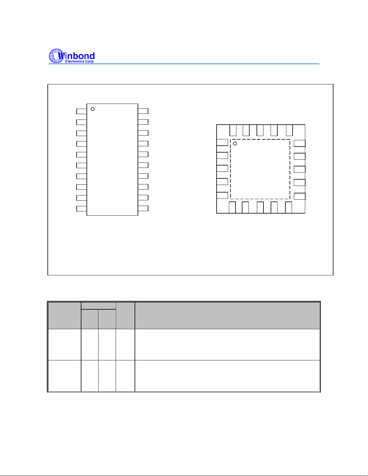
2. PIN CONFIGURATION AND DESCRIPTION
(Top
W83L351 Series
SYSRST#
SHDN#
STBY#
3.3VIN
3.3VIN
3.3VOUT
3.3VOUT
PERST#
NC
GND
1
2
3
4
5
6
7
8
9
10
W83L351G
(Top View)
20
19
18
17
16
15
14
13
12
11
OC#
RCLKEN
AUXIN
AUXOUT
1.5VIN
1.5VIN
1.5VOUT
1.5VOUT
CPPE#
CPUSB#
STBY#
3.3VOUT
3.3VIN
NC
NC
SHDN#
20
1
2
3
4
5
6
SYSRST#
RCLKEN
OC#
19
7
GND
AUXIN
NC
18
8
PERST#
16
17
15
AUXOUT
NC
14
13
NC
12
1.5VIN
11
10
9
CPPE#
CPUSB#
1.5VOUT
W83L351YG
W83L351YCG
View)
PIN
SYMBOL
G
YG
YCG
SYSRST# 1 6 I
SHDN# 2 20 I
I/O FUNCTION
System Reset input – active low, logic level signal. Internally pulled
up to AUXIN. This input is driven by the host system and directly
(*)
affects PERST#. Asserting SYSRST# (logic low) forces PERST# to
assert. RCLKEN is not affected by the assertion of SYSRST#.
Shutdown input – active low, logic level signal. Internally pulled up
to AUXIN. When asserted (logic low), this input instructs the power
(*)
switch to turn off all voltage outputs and the discharge FETs are
activated.
-2-
Continued
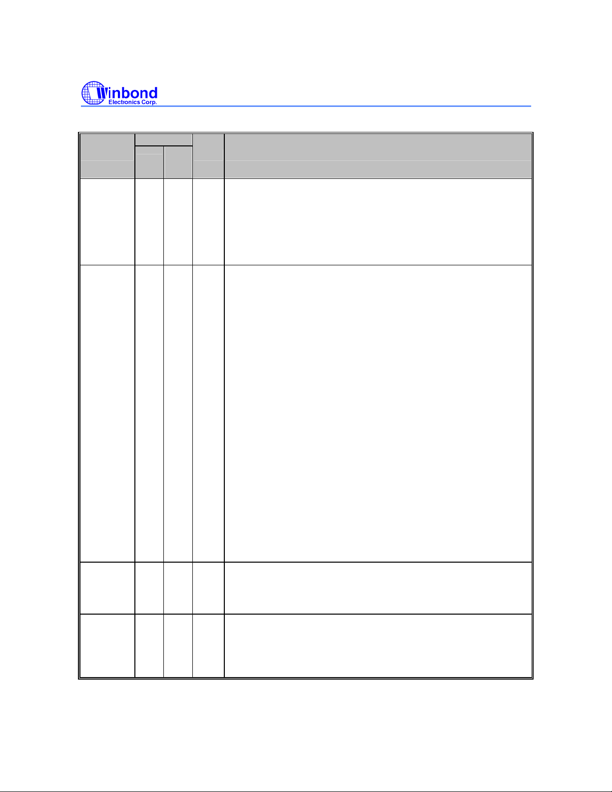
PIN
SYMBOL
STBY# 3 1 I
PERST# 8 8 O
G
YG
YCG
I/O FUNCTION
(*)
W83L351 Series
Standby input – active low, logic level signal. Internally pulled up to
AUXIN. When asserted (logic low) after the card is inserted, this
input places the power switch in standby mode by turning off the
3.3V and 1.5V power switches and keeping the AUX switch on. If
the signal is asserted prior to the card being present, STBY#
places the power switch in OFF Mode by turning off the AUX, 3.3V,
and 1.5V power switches.
A logic level power good (with delay). When powered up, this
output remains asserted (logic level low) until all power rails are
within the tolerance. Once all power rails are within the tolerance
and RCLKEN has been released (logic high), PERST# is deasserted (logic high) after a time delay, as shown in the parametric
table. When powered down, this output is asserted whenever any
of the power rails drops below their voltage tolerance.
The PERST# signal is an output from the host system and an input
to the ExpressCard module. This signal is only used by PCI
Express-based modules and its function is to place the
ExpressCard module in a reset state.
During power up, power down, or whenever power to the
ExpressCard module is not stable or not within voltage tolerance
limits, the ExpressCard standard requires that PERST# be
asserted. As a result, this signal also serves as a power-good
indicator to the ExpressCard module, and the relationship between
the power rails and PERST# are explicitly defined in the
ExpressCard standard.
The host can also place the ExpressCard module in a reset state
by asserting a system reset SYSRST#. This system reset
generates a PERST# signal to the ExpressCard module without
disrupting the voltage rails. This is normally called a warm reset.
However, in a cold start situation, the system reset can also be
used to prolong the assertion time of PERST#.
CPUSB# 11 9 I
CPPE# 12 10 I
-3- Revision 1.10
Card Present input for USB cards. Internally pulled up to AUXIN. A
logic low level on this input indicates that the card present supports
(*)
the USB functions. When a card is inserted, CPUSB# is physically
connected to ground if the card supports USB functions.
Card Present input for PCI Express cards. Internally pulled up to
AUXIN. A logic low level on this input indicates that the card
(*)
present supports the PCI Express functions. When a card is
inserted, CPPE# is physically connected to ground if the card
supports PCI Express functions.
Publication Date: July 5, 2007
W83L351 Series
Continued
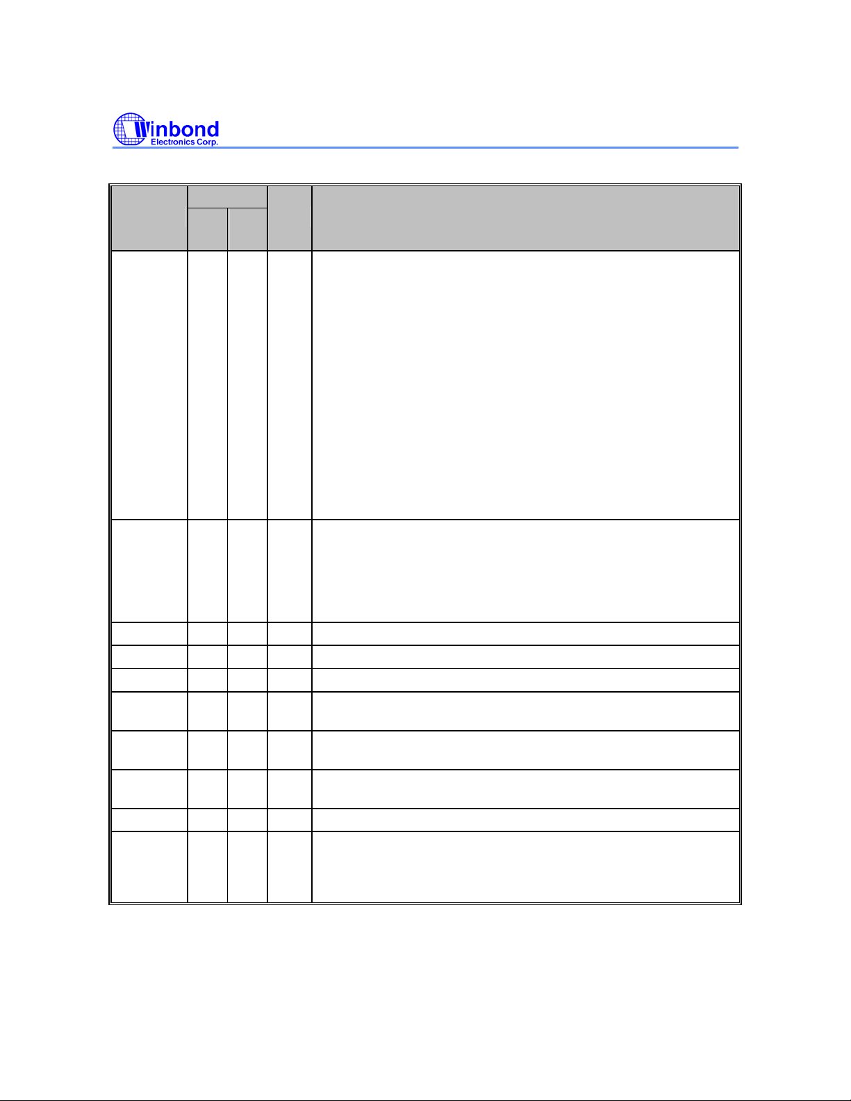
PIN
SYMBOL
RCLKEN 19 18 I
OC# 20 19 OD
3.3VIN 4, 5 2 I Primary voltage source, 3.3V input for 3.3VOUT
1.5VIN 15,16 12 I Secondary voltage source, 1.5V input for 1.5VOUT
AUXIN 18 17 I Auxiliary voltage source, AUX input for AUXOUT and chip power.
3.3VOUT 6, 7 3 O
1.5VOUT
AUXOUT 17 15 O
GND 10 7 Ground
NC 9
Notice:
(*)
Be aware that no input pins can be driven HIGH before the Auxiliary voltage is VALID.
G
13,
14
YG
YCG
4, 5,
13,
14,
I/O FUNCTION
Reference Clock Enable signal. As an output, it is a logic level
power good to the host (no delay – open drain). As an input, if the
signal is kept inactive (low) by the host, PERST# will be prevented
from being de-asserted. Internally pulled up to AUXIN. This pin
serves both as an input and an output. When powered up, a
discharge FET keeps this signal at a low state as long as any of the
output power rails is out of their tolerance range. Once all output
power rails are within the tolerance, the switch releases RCLKEN,
(*)
/O
allowing it to transit to a high state (internally pulled up to AUXIN).
The transition of RCLKEN from a low to a high state starts an
internal timer for the purpose of de-asserting PERST#. As an input,
RCLKEN can be kept low to delay the start of the PERST# internal
timer. Because RCLKEN is internally connected to a discharge
FET, this pin can only be driven low and should never be driven
high as a logic input. When an external circuit drives this pin low,
RCLKEN becomes an input; otherwise, this pin is an output.
Over current status output (open drain). This pin is an open-drain
output. When any of the three power switches (AUX, 3.3V, and
1.5V) is in an over current condition, OC# is asserted (logic low) by
an internal discharge FET with a deglitch delay. Otherwise, the
discharge FET is open, and the pin can be pulled up to a power
supply through an external resistor.
Switched output that delivers 0V, 3.3V or high impedance to the
card.
11 O
16
Switched output that delivers 0V, 1.5V or high impedance to the
card.
Switched output that delivers 0V, AUX or high impedance to the
card.
No connection
-4-
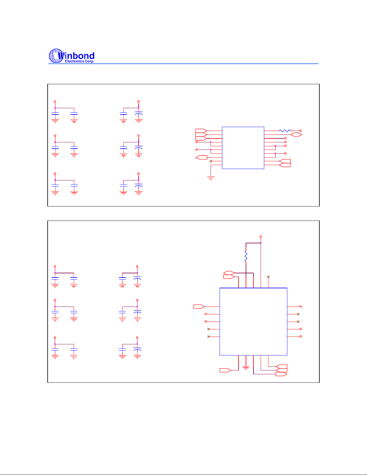
3. APPLICATION CIRCUIT
AUXIN
AUXOUT
W83L351 Series
3.3VIN
1.5VIN
AUXIN
3.3VIN
C1
0.1U
C5
0.1U
C9
0.1U
C1
0.1U
C5
0.1U
C2
4.7U
C6
4.7U
C10
4.7U
C2
4.7U
C6
4.7U
C3
0.1U
3.3VOUT
C7
0.1U
1.5VOUT
C11
0.1U
AUXOUT
C3
0.1U
3.3VOUT
C7
0.1U
1.5VOUT1.5VIN
C4
22U
C8
22U
C12
22U
C4
22U
C8
22U
SY SRST#
SHDN #
STBY#
3.3VIN
3.3VOUT
PERST#
STBY#
3.3VIN
3.3VOUT
1
2
3
4
5
6
7
8
9
10
RCLKEN
SHDN#
1
2
3
4
5
U1
SYSR ST#
SHDN#
STBY#
3.3VIN
3.3VIN
3.3VOUT
3.3VOUT
PERST#
NC
GND
U1
STBY#
3.3VI N
3.3VOUT
NC
NC
20
OC#
AUXIN
1.5VI N
1.5VI N
CPPE#
AUXIN
RCLKEN
19
18
17
16
15
14
13
12
11
AUXI N
RCLKEN
AUXOUT
1.5VOU T
1.5VOU T
CPUSB#
W83L351G
R1
2K
2019181716
OC#
SHDN#
W83L351YG/YCG
NC
AUXOUT
1.5VI N
1.5VOUT
NC
NC
R1
2K
AUXIN
AUXOUT
1.5VIN
1.5VOUT
CPPE#
CPUSB#
15
14
13
12
11
AUXIN
RCLKEN
AUXOUT
1.5VIN
1.5VOUT
C9
0.1U
C10
4.7U
C11
0.1U
C12
22U
SYSR ST#
SYSRST#
GND
PERST#
CPUSB#
CPPE#
6
7
8
9
10
CPPE#
CPUSB#
PERST#
Publication Date: July 5, 2007
-5- Revision 1.10
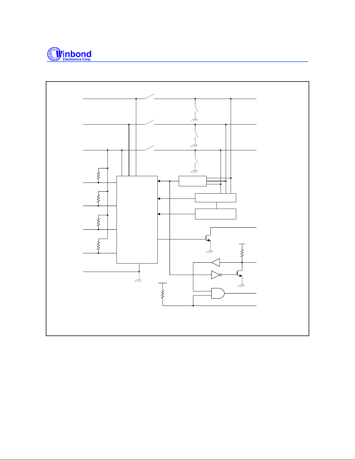
4. INTERNAL BLOCK DIAGRAM
W83L351 Series
1.5VI N
3.3VIN
AUXIN
CPUSB #
CPPE #
STBY #
SHDN #
GND
SW1
SW2
SW3
Control Logic
1.5VOUT
SW4
3.3VOUT
SW5
AUXOUT
SW6
Detctor
Current Limit
Thermal protection
OC #
AUXIN
RCLKEN
POWER_GOOD_ALL
AUXIN
PERST #
SYSRST #
-6-

5. ABSOLUTE MAXIMUM RATINGS
ITEM SYMBOL RATING UNIT
W83L351 Series
Input Voltage
V
V
V
-0.3 to 6 V
I(3.3VIN)
-0.3 to 6 V
I(1.5VIN)
-0.3 to 6 V
I(AUXIN)
Logic Input/Output Voltage -0.3 to 6 V
V
O(3.3VOUT)
Output Voltage
Output Current
V
O(1.5VOUT)
V
O(AUXOUT)
I
O(3.3OUT)
I
O(1.5OUT)
I
O(AUXOUT)
Operating Temperature Range T
Human Body Mode
Electrostatic discharge protection
Machine Mode
Latch-Up
-0.3 to 6 V
-0.3 to 6 V
-0.3 to 6 V
Internally limited
Internally limited
Internally limited
0 to 70
opt
±2
℃
kV
±200
±100
mA
V
Publication Date: July 5, 2007
-7- Revision 1.10
 Loading...