winbond W83697HF Technical data

WINBOND
LPC I/O
W83697HF
Revision: 2.0 Date: April 14, 2005

W83697HF
Table of Contents-
1. GENERAL DESCRIPTION ......................................................................................................... 2
2. FEATURES ................................................................................................................................. 2
3. BLOCK DIAGRAM ...................................................................................................................... 5
4. PIN CONFIGURATION............................................................................................................... 6
5. PIN DESCRIPTION..................................................................................................................... 7
5.1 LPC Interface.................................................................................................................. 8
5.2 FDC Interface ................................................................................................................. 9
5.3 Multi-Mode Parallel Port ............................................................................................... 10
5.4 Serial Port Interface ...................................................................................................... 15
5.5 Infrared Port.................................................................................................................. 16
5.6 Flash ROM Interface..................................................................................................... 16
5.7 Hardware Monitor Interface .......................................................................................... 17
5.8 Game Port & MIDI Port................................................................................................. 18
5.9 Power Pins.................................................................................................................... 19
6. HARDWARE MONITOR ........................................................................................................... 19
6.1 General Description...................................................................................................... 19
6.2 Access Interface ........................................................................................................... 19
6.3 Analog Inputs................................................................................................................ 21
6.4 FAN Speed Count and FAN Speed Control ................................................................. 24
6.5 SMI# Interrupt Mode ..................................................................................................... 27
6.6 OVT# Interrupt Mode .................................................................................................... 29
6.7 REGISTERS AND RAM ............................................................................................... 30
7. CONFIGURATION REGISTER ................................................................................................ 59
7.1 Plug and Play Configuration ......................................................................................... 59
7.2 Compatible PnP............................................................................................................ 59
7.3 Configuration Sequence ............................................................................................... 60
7.4 Chip (Global) Control Register ..................................................................................... 62
7.5 Logical Device 0 (FDC)................................................................................................. 66
7.6 Logical Device 1 (Parallel Port) .................................................................................... 69
7.7 Logical Device 2 (UART A)........................................................................................... 70
7.8 Logical Device 3 (UART B)........................................................................................... 71
7.9 Logical Device 6 (CIR).................................................................................................. 72
7.10 Logical Device 7 (Game Port GPIO Port 1).................................................................. 73
7.11 Logical Device 8 (MIDI Port and GPIO Port 5)............................................................. 73
7.12 Logical Device 9 (GPIO Port 2 ~ GPIO Port 4 ) ........................................................... 75
7.13 Logical Device A (ACPI) ............................................................................................... 76
Publication Release Date: April 14, 2005
- I - Revision 2.0

W83697HF
7.14 Logical Device B (Hardware Monitor)........................................................................... 80
8. ELECTRICAL CHARACTERISTICS......................................................................................... 81
8.1 Absolute Maximum Ratings.......................................................................................... 81
8.2 DC Characteristics........................................................................................................ 81
9. APPLICATION CIRCUITS ........................................................................................................ 89
9.1 Parallel Port Extension FDD......................................................................................... 89
9.2 Parallel Port Extension 2FDD....................................................................................... 90
9.3 Four FDD Mode ............................................................................................................ 90
10. ORDERING INSTRUNCTION .................................................................................................. 91
11. HOW TO READ THE TOP MARKING...................................................................................... 91
12. PACKAGE DIMENSIONS......................................................................................................... 92
13. APPENDIX A: DEMO CIRCUIT ................................................................................................ 93
- II -

W83697HF
1. GENERAL DESCRIPTION
The W83697HF is evolving product from Winbond's most popular I/O family. They feature a whole
new interface, namely LPC (Low Pin Count) interface, which will be supported in the new generation
chip-set. This interface as its name suggests is to provide an economical implementation of I/O's
interface with lower pin count and still maintains equivalent performance as its ISA interface
counterpart. Approximately 40 pin counts are saved in LPC I/O comparing to ISA implementation.
With this additional freedom, we can implement more devices on a single chip as demonstrated in
W83697HF's integration of Game Port and MIDI Port. It is fully transparent in terms of software which
means no BIOS or device driver update is needed except chip-specific configuration.
The disk drive adapter functions of W83697HF include a floppy disk drive controller compatible with
the industry standard 82077/ 765, data separator, write pre-compensation circuit, decode logic, data
rate selection, clock generator, drive interface control logic, and interrupt and DMA logic. The wide
range of functions integrated onto the W83697HF greatly reduces the number of components required
for interfacing with floppy disk drives. The W83697HF supports four 360K, 720K, 1.2M, 1.44M, or
2.88M disk drives and data transfer rates of 250 Kb/s, 300 Kb/s, 500 Kb/s, 1 Mb/s, and 2 Mb/s.
The W83697HF provides two high-speed serial communication ports (UARTs), one of which supports
serial Infrared communication. Each UART includes a 16-byte send/receive FIFO, a programmable
baud rate generator, complete modem control capability, and a processor interrupt system. Both
UARTs provide legacy speed with baud rate up to 115.2k bps and also advanced speed with baud
rates of 230k, 460k, or 921k bps which support higher speed modems. In addition, the W83697HF
provides IR functions: IrDA 1.0 (SIR for 1.152K bps) and TV remote IR (Consumer IR, supporting
NEC, RC-5, extended RC-5, and RECS-80 protocols).
The W83697HF supports one PC-compatible printer port (SPP), Bi-directional Printer port (BPP) and
also Enhanced Parallel Port (EPP) and Extended Capabilities Port (ECP). Through the printer port
interface pins, also available are: Extension FDD Mode and Extension 2FDD Mode allowing one or
two external floppy disk drives to be connected.
The configuration registers support mode selection, function enable/disable, and power down function
selection. Furthermore, the configurable PnP features are compatible with the plug-and-play feature
demand of Windows 95/98TM, which makes system resource allocation more efficient than ever.
The W83697HF provides a set of flexible I/O control functions to the system designer through a set of
General Purpose I/O ports. These GPIO ports may serve as simple I/O or may be individually
configured to provide a predefined alternate function. General Purpose Port 1 is designed to be
functional even in power down mode (VCC is off).
©
The W83697HF is made to fully comply with Microsoft
meet the requirements of ACPI.
The W83697HF contains a game port and a MIDI port. The game port is designed to support 2
joysticks and can be applied to all standard PC game control devices, They are very important for a
entertainment or consumer computer.
The W83697HF provides Flash ROM interface. That can support up to 4M legacy flash ROM.
The W83697HF support hardware status monitoring for personal computers. It can be used to monitor
several critical hardware parameters of the system, including power supply voltages, fan speeds, and
temperatures, which are very important for a high-end computer system to work stably and properly.
Moreover, W83697HF support the Smart Fan control system, including the thermal Cruise
speed Cruise
TM
” functions. Smart Fan can make system more stable and user friendly.
PC98 and PC99 Hardware Design Guide, and
TM
” and
- 2 -

2. FEATURES
General
• Meet LPC Spec. 1.01
• Support LDRQ#(LPC DMA), SERIRQ (serial IRQ)
• Include all the features of Winbond I/O W83877TF
• Integrate Hardware Monitor functions
• Compliant with Microsoft PC98/PC99 Hardware Design Guide
• Support DPM (Device Power Management), ACPI
• Programmable configuration settings
• Single 24 or 48 MHz clock input
FDC
• Compatible with IBM PC AT disk drive systems
• Variable write pre-compensation with track selectable capability
• Support vertical recording format
W83697HF
• DMA enable logic
• 16-byte data FIFOs
• Support floppy disk drives and tape drives
• Detects all overrun and under run conditions
• Built-in address mark detection circuit to simplify the read electronics
• FDD anti-virus functions with software write protect and FDD write enable signal (write data signal
was forced to be inactive)
• Support up to four 3.5-inch or 5.25-inch floppy disk drives
• Completely compatible with industry standard 82077
• 360K/720K/1.2M/1.44M/2.88M format; 250K, 300K, 500K, 1M, 2M bps data transfer rate
• Support 3-mode FDD, and its Win95/98 driver
UART
• Two high-speed 16550 compatible UARTs with 16-byte send/receive FIFOs
• MIDI compatible
• Fully programmable serial-interface characteristics:
--- 5, 6, 7 or 8-bit characters
--- Even, odd or no parity bit generation/detection
--- 1, 1.5 or 2 stop bits generation
• Internal diagnostic capabilities:
--- Loop-back controls for communications link fault isolation
- 2 -

W83697HF
--- Break, parity, overrun, framing error simulation
16
• Programmable baud generator allows division of 1.8461 MHz and 24 MHz by 1 to (2
• Maximum baud rate up to 921k bps for 14.769 MHz and 1.5M bps for 24 MHz
Infrared
• Support IrDA version 1.0 SIR protocol with maximum baud rate up to 115.2K bps
• Support SHARP ASK-IR protocol with maximum baud rate up to 57,600 bps
• Support Consumer IR with Wake-Up function.
Parallel Port
• Compatible with IBM parallel port
• Support PS/2 compatible bi-directional parallel port
• Support Enhanced Parallel Port (EPP) − Compatible with IEEE 1284 specification
• Support Extended Capabilities Port (ECP) − Compatible with IEEE 1284 specification
• Extension FDD mode supports disk drive B; and Extension 2FDD mode supports disk drives A
and B through parallel port
-1)
• Enhanced printer port back-drive current protection
Game Port
• Support two separate Joysticks
• Support every Joystick two axes (X, Y) and two buttons (S1,S2) controllers
MIDI Port
• The baud rate is 31.25 K baud rate
• 16-byte input FIFO
• 16-byte output FIFO
Flash ROM Interface
• Support up to 4M flash ROM
General Purpose I/O Ports
• 48 programmable general purpose I/O ports
• General purpose I/O ports can serve as simple I/O ports, watch dog timer output, power LED
output, infrared I/O pins, suspend LED output, Beep output
• Functional in power down mode
Publication Release Date: April 14, 2005
- 3 - Revision2.0

W83697HF
Hardware Monitor Functions
• Smart fan control system, support thermal CruiseTM” and speed CruiseTM”
• 2 thermal inputs from optionally remote thermistors or 2N3904 transistors or Pentium
thermal diode output
• 6 positive voltage inputs (typical for +12V, -12V, +5V, -5V, +3.3V, Vcore)
• 2 intrinsic voltage monitoring (typical for Vbat, +5VSB)
• 2 fan speed monitoring inputs
• 2 fan speed control
• Build in Case open detection circuit
• WATCHDOG comparison of all monitored values
• Programmable hysteresis and setting points for all monitored items
• Over temperature indicate output
• Automatic Power On voltage detection Beep
• Issue SMI#, IRQ, OVT# to activate system protection
TM
• Winbond Hardware Doctor
• Intel LDCM
TM
/ Acer ADMTM compatible
Package
• 128-pin PQFP
Support
TM
II/III
- 4 -
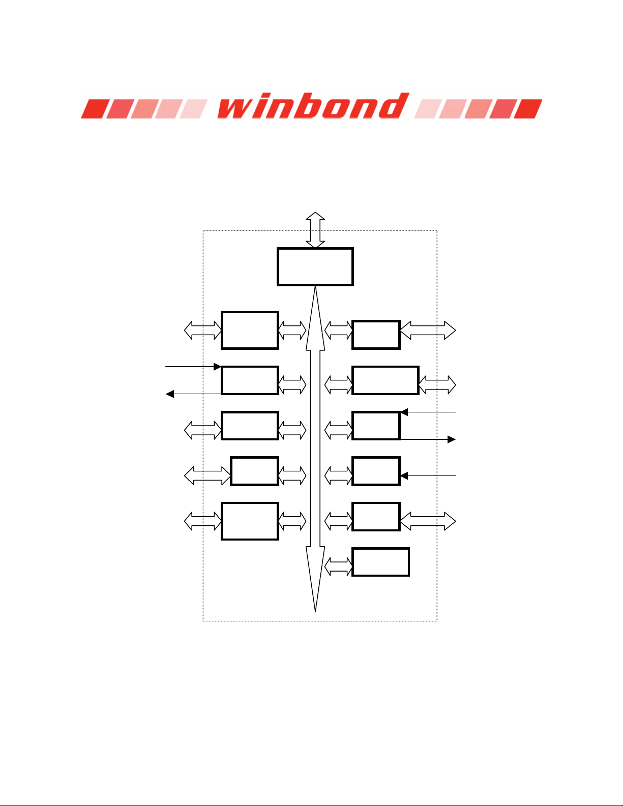
3. BLOCK DIAGRAM
W83697HF
Joystick interface
signals
MSO
General-purpose
I/O pins
Hardware monitor
channel and Vref
LRESET#, LCLK, LFRAME#, LAD[3:0], LDRQ#, SERIRQ
LPC
Interface
Game
Port
FDC
MSI
MIDI
URA, B
GPIO IR
HM CIR
Floppy drive
interface signals
Serial port A, B
interface signals
IRRX
IRTX
CIRRX#
Flash ROM
interface signals
Flash
ROM
PRT
Printer port
interface signals
ACPI
Publication Release Date: April 14, 2005
- 5 - Revision2.0
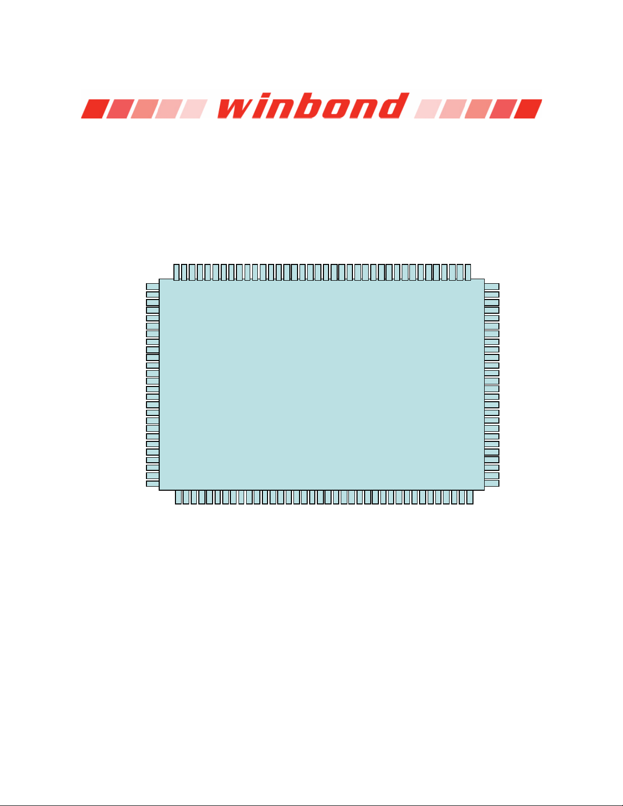
4. PIN CONFIGURATION
VBAT
CASEOPEN#
VSB
PME#
CASEOPEN#
VSB
PME#
CASEOPEN#
VSB
PME#
CASEOPEN#
VSB
PME#
CIRRX
ME MW# /GP 52
CIRRX
ME MW# /GP 52
CIRRX
ME MW# /GP 52
CIRRX
ME MW# /GP 52
999897
999897
999897
999897
999897
101
101
101
101
101
100
100
100
100
100
1
1
1
1
2
345
345
345
345
6789101112
6789101112
6789101112
6789101112
2
2
2
VTIN2
VTIN2
VTIN2
VTIN2
VTIN1
VTIN1
VTIN1
VTIN1
AVCC
AVCC
AVCC
AVCC
VREF
VREF
VREF
VREF
VCORE
VCORE
VCORE
VCORE
+3.3VI N
+3.3VI N
+3.3VI N
+3.3VI N
+12VI N
+12VI N
+12VI N
+12VI N
-12VIN
-12VIN
-12VIN
-12VIN
-5VIN
-5VIN
-5VIN
-5VIN
AGND
AGND
AGND
AGND
FANIO2
FANIO2
FANIO2
FANIO2
FANIO1
FANIO1
FANIO1
FANIO1
FANPWM2
FANPWM2
FANPWM2
FANPWM2
FANPWM1
FANPWM1
FANPWM1
FANPWM1
OVT#/SMI#
OVT#/SMI#
OVT#/SMI#
OVT#/SMI#
BEEP
BEEP
BEEP
MSI /G P51/ WD TO#
MSI /G P51/ WD TO#
MSO/GP50/PLED
MSO/GP50/PLED
MSO/GP50/PLED
MSO/GP50/PLED
BEEP
GPAS2/GP17
GPAS2/GP17
GPAS2/GP17
GPAS2/GP17
GPBS2/GP16
GPBS2/GP16
GPBS2/GP16
GPBS2/GP16
GPAY/GP15
GPAY/GP15
GPAY/GP15
GPAY/GP15
GPBY/GP14
GPBY/GP14
GPBY/GP14
GPBY/GP14
GPBX/GP13
GPBX/GP13
GPBX/GP13
GPBX/GP13
GPAX/GP12
GPAX/GP12
GPAX/GP12
GPAX/GP12
GPBS1/GP11
GPBS1/GP11
GPBS1/GP11
GPBS1/GP11
GPAS1/GP10
GPAS1/GP10
GPAS1/GP10
GPAS1/GP10
103
103
103
103
103
104
104
104
104
104
105
105
105
105
105
106
106
106
106
106
107
107
107
107
107
108
108
108
108
108
109
109
109
109
109
110
110
110
110
110
111
111
111
111
111
112
112
112
112
112
113
113
113
113
113
114
114
114
114
114
115
115
115
115
115
116
116
116
116
116
117
117
117
117
117
118
118
118
118
118
119
119
119
119
119
120
120
120
120
120
121
121
121
121
121
122
122
122
122
122
123
123
123
123
123
124
124
124
124
124
125
125
125
125
125
126
126
126
126
126
127
127
127
127
127
128
128
128
128
128
VBAT
VBAT
VBAT
102
102
102
102
102
ME MR#G P53
ROMCS#/GP54
ME MR#G P53
ROMCS#/GP54
ME MR#G P53
ROMCS#/GP54
ME MR#G P53
ROMCS#/GP54
969594
969594
969594
969594
969594
XD O/ G P 2 0
XD 1/ G P 21
XD 2/ G P 22
XD 3/ G P 23
GND
XD 4/ G P 24
XD 5/ G P 25
XD 6/ G P 26
XD O/ G P 2 0
XD 1/ G P 21
XD 2/ G P 22
XD 3/ G P 23
XD O/ G P 2 0
XD O/ G P 2 0
GND
XD 1/ G P 21
XD 2/ G P 22
XD 3/ G P 23
GND
XD 1/ G P 21
XD 2/ G P 22
XD 3/ G P 23
GND
939291
908988
939291
908988
939291
908988
939291
908988
939291
908988
W83697HF
W83697HF
W83697HF
W83697HF
XD 4/ G P 24
XD 5/ G P 25
XD 4/ G P 24
XD 5/ G P 25
XD 4/ G P 24
XD 5/ G P 25
131415
131415
131415
131415
XD 7/ G P 27
XD 6/ G P 26
XD 7/ G P 27
XD 6/ G P 26
XD 7/ G P 27
XD 6/ G P 26
XD 7/ G P 27
878685
878685
878685
878685
878685
161718
161718
161718
161718
XA0/G P30
XA1/G P31
XA2/G P32
XA3/G P33
XA4/G P34
XA5/G P35
XA6/G P36
XA7/G P37
XA8/G P40
XA9/G P41
XA 1 0/ G P 42
XA 1 2/ G P 44
XA 1 3/ G P 45
XA0/G P30
XA1/G P31
XA2/G P32
XA3/G P33
XA4/G P34
XA5/G P35
XA6/G P36
XA7/G P37
XA8/G P40
XA9/G P41
XA0/G P30
XA1/G P31
XA2/G P32
XA3/G P33
XA4/G P34
XA5/G P35
XA6/G P36
XA0/G P30
XA1/G P31
XA2/G P32
XA3/G P33
848382
848382
848382
848382
848382
19202122232425262728293031323334353637
19202122232425262728293031323334353637
19202122232425262728293031323334353637
19202122232425262728293031323334353637
XA4/G P34
XA5/G P35
818079
818079
818079
818079
818079
XA7/G P37
XA6/G P36
XA7/G P37
787776
787776
787776
787776
787776
XA8/G P40
XA8/G P40
XA9/G P41
XA9/G P41
VCC
VCC
VCC
VCC
757473
757473
757473
757473
757473
XA 1 0/ G P 42
XA 1 0/ G P 42
XA 1 0/ G P 42
XA 1 1 / G P4 3
XA 1 1 / G P4 3
XA 1 1 / G P4 3
XA 1 1 / G P4 3
XA 1 2/ G P 44
XA 1 3/ G P 45
XA 1 2/ G P 44
XA 1 3/ G P 45
XA 1 2/ G P 44
XA 1 3/ G P 45
727170
727170
727170
727170
727170
XA 1 5/ G P 47
XA 1 5/ G P 47
XA 1 5/ G P 47
XA 1 5/ G P 47
XA 1 4 / G P4 6
XA 1 4 / G P4 6
XA 1 4 / G P4 6
XA 1 4 / G P4 6
696867
696867
696867
696867
696867
W83697HF
XA 1 6/ G P 55
XA 1 8/ G P 57
IRTX
XA 1 6/ G P 55
XA 1 8/ G P 57
IRTX
XA 1 6/ G P 55
XA 1 8/ G P 57
IRTX
XA 1 6/ G P 55
XA 1 8/ G P 57
IRTX
XA 1 7 / G P5 6
XA 1 7 / G P5 6
XA 1 7 / G P5 6
XA 1 7 / G P5 6
66
66
66
66
66
65
65
65
65
65
64
64
64
64
64
IRRX
IRRX
IRRX
IRRX
63
63
63
63
63
RIB#
RIB#
RIB#
RIB#
62
62
62
62
62
DCDB#
DCDB#
DCDB#
DCDB#
61
61
61
61
61
SOUTB/PEN48
SOUTB/PEN48
SOUTB/PEN48
SOUTB/PEN48
60
60
60
60
60
GND
GND
GND
GND
59
59
59
59
59
SINB
SINB
SINB
SINB
58
58
58
58
58
DTRB#
DTRB#
DTRB#
DTRB#
57
57
57
57
57
RTSB#
RTSB#
RTSB#
RTSB#
56
56
56
56
56
DSRB#
DSRB#
DSRB#
DSRB#
55
55
55
55
55
CTSB#
CTSB#
CTSB#
CTSB#
54
54
54
54
54
RIA#
RIA#
RIA#
RIA#
53
53
53
53
53
DCDA#
DCDA#
DCDA#
DCDA#
52
52
52
52
52
SOUTA/PENROM#
SOUTA/PENROM#
SOUTA/PENROM#
SOUTA/PENROM#
51
51
51
51
51
SINA
SINA
SINA
SINA
50
50
50
50
50
DTRA#/PNPC SV#
DTRA#/PNPC SV#
DTRA#/PNPC SV#
DTRA#/PNPC SV#
49
49
49
49
49
RTSA#/HEFRAS
RTSA#/HEFRAS
RTSA#/HEFRAS
RTSA#/HEFRAS
48
48
48
48
48
DSRA#
DSRA#
DSRA#
DSRA#
47
47
47
47
47
CTSA#
CTSA#
CTSA#
CTSA#
46
46
46
46
46
STB#
STB#
STB#
STB#
45
45
45
45
45
VCC
VCC
VCC
VCC
44
44
44
44
44
AFD#
AFD#
AFD#
AFD#
43
43
43
43
43
INIT#
INIT#
INIT#
INIT#
42
42
42
42
42
PD0
PD0
PD0
PD0
41
41
41
41
41
PD1
PD1
PD1
PD1
40
40
40
40
40
PD2
PD2
PD2
PD2
39
39
39
39
39
PD3
PD3
PD3
PD3
38
38
38
38
PE
PE
PE
RVDEN0
RVDEN0
RVDEN0
RVDEN0
VCC
VCC
VCC
VCC
DIR#
WE#
DIR#
DIR#
DSA#
DSA#
DSA#
DSA#
DIR#
MOB #
MOB #
MOB #
MOB #
STEP#
STEP#
STEP#
STEP#
DSB#
DSB#
DSB#
DSB#
MOA#
MOA#
MOA#
MOA#
INDEX#
INDEX#
INDEX#
INDEX#
WP#
WE#
WP#
WE#
WP#
WE#
WP#
WD#
WD#
WD#
WD#
TRAK0#
TRAK0#
TRAK0#
TRAK0#
RDATA#
RDATA#
RDATA#
RDATA#
GND
GND
GND
GND
CLKIN
CLKIN
CLKIN
CLKIN
HEAD#
HEAD#
HEAD#
HEAD#
PCICLK
PCICLK
PCICLK
PCICLK
SKCHG#
SKCHG#
SKCHG#
SKCHG#
LAD3
LAD0
LAD3
LAD0
LAD3
LAD0
LAD3
LAD0
LAD2
LAD1
LAD2
LAD1
LAD2
LAD1
LAD2
LAD1
VCC3
VCC3
VCC3
VCC3
LDRQ#
LDRQ#
LDRQ#
LDRQ#
SERIRQ
SERIRQ
SERIRQ
SERIRQ
FRAME#
FRAME#
FRAME#
FRAME#
PE
SLCT
SLCT
SLCT
SLCT
BUSY
BUSY
BUSY
BUSY
LRESET#
LRESET#
LRESET#
LRESET#
ACK#
ACK#
ACK#
ACK#
PD7
PD6
PD5
PD4
PD7
PD6
PD5
PD4
PD7
PD6
PD5
PD4
PD7
PD6
PD5
ERR#
SLIN#
ERR#
SLIN#
ERR#
SLIN#
ERR#
SLIN#
PD4
- 6 -

5. PIN DESCRIPTION
Note: Please refer to Section 10.2 DC CHARACTERISTICS for details
PIN DESCRIPTION
I/O8t
I/O
12t
I/O
24t
I/O
I/O
I/O
I/O
I/OD
I/OD
I/OD
I/OD
I/OD
I/OD
I/OD
I/OD
I/OD
I/OD
I/OD
O4
O8
O12
O16
O24
O
O
OD8
OD12
OD24
OD
12tp3
12ts
24ts
24tsp3
12t
24t
24c
24a
12ts
24ts
12cs
16cs
24cs
12csd
12csu
12p3
24p3
12p3
TTL level bi-directional pin with 8mA source-sink capability
TTL level bi-directional pin with 12mA source-sink capability
TTL level bi-directional pin with 24 mA source-sink capability
3.3V TTL level bi-directional pin with 12mA source-sink capability
TTL level Schmitt-trigger bi-directional pin with 12mA source-sink capability
TTL level Schmitt-trigger bi-directional pin with 24mA source-sink capability
3.3V TTL level Schmitt-trigger bi-directional pin with 24mA source-sink capability
TTL level bi-directional pin and open-drain output with 12mA sink capability
TTL level bi-directional pin and open-drain output with 24mA sink capability
CMOS level bi-directional pin and open-drain output with 24mA sink capability
Bi-directional pin with analog input and open-drain output with 24mA sink capability
TTL level Schmitt-trigger bi-directional pin and open-drain output with 12mA sink capability
TTL level Schmitt-trigger bi-directional pin and open-drain output with 24mA sink capability
CMOS level Schmitt-trigger bi-directional pin and open-drain output with 12mA sink capability
CMOS level Schmitt-trigger bi-directional pin and open-drain output with 16mA sink capability
CMOS level Schmitt-trigger bi-directional pin and open-drain output with 24mA sink capability
CMOS level Schmitt-trigger bi-directional pin with internal pull down resistor and open-drain output with
12mA sink capability
CMOS level Schmitt-trigger bi-directional pin with internal pull up resistor and open-drain output with
12mA sink capability
Output pin with 4 mA source-sink capability
Output pin with 8 mA source-sink capability
Output pin with 12 mA source-sink capability
Output pin with 16 mA source-sink capability
Output pin with 24 mA source-sink capability
3.3V output pin with 12 mA source-sink capability
3.3V output pin with 24 mA source-sink capability
Open-drain output pin with 8 mA sink capability
Open-drain output pin with 12 mA sink capability
Open-drain output pin with 24 mA sink capability
3.3V open-drain output pin with 12 mA sink capability
W83697HF
Publication Release Date: April 14, 2005
- 7 - Revision2.0

INt
IN
tp3
INtd
INtu
INts
IN
tsp3
INc
INcu
INcd
INcs
IN
csu
W83697HF
PIN DESCRIPTION
TTL level input pin
3.3V TTL level input pin
TTL level input pin with internal pull down resistor
TTL level input pin with internal pull up resistor
TTL level Schmitt-trigger input pin
3.3V TTL level Schmitt-trigger input pin
CMOS level input pin
CMOS level input pin with internal pull up resistor
CMOS level input pin with internal pull down resistor
CMOS level Schmitt-trigger input pin
CMOS level Schmitt-trigger input pin with internal pull up resistor
5.1 LPC Interface
SYMBOL PIN I/O FUNCTION
CLKIN 17 IN
PME#
98 OD
PCICLK 19 IN
LDRQ# 20 O
SERIRQ 21 I/O12tp3 Serial IRQ input/Output.
LAD[3:0] 23-
26
LFRAME#
LRESET#
27 IN
28 IN
System clock input. According to the input frequency 24MHz or
tp3
48MHz, it is selectable through register. Default is 24MHz input.
Generated PME event.
12p3
PCI clock 33 MHz input.
tsp3
Encoded DMA Request signal.
12p3
I/O
These signal lines communicate address, control, and data
12tp3
information over the LPC bus between a host and a peripheral.
Indicates start of a new cycle or termination of a broken cycle.
tsp3
Reset signal. It can connect to PCIRST# signal on the host.
tsp3
- 8 -

5.2 FDC Interface
SYMBOL PIN I/O FUNCTION
OD
IN
OD
OD
OD
OD
OD
OD
OD
OD
IN
IN
IN
OD
IN
24
csu
24
24
24
24
24
24
24
24
csu
csu
csu
24
csu
Drive Density Select bit 0.
This Schmitt-triggered input from the disk drive is active low
when the head is positioned over the beginning of a track marked
by an index hole. This input pin is pulled up internally by a 1 KΩ
resistor. The resistor can be disabled by bit 7 of L0-CRF0
(FIPURDWN).
Motor A On. When set to 0, this pin enables disk drive 0. This is
an open drain output.
Drive Select B. When set to 0, this pin enables disk drive B. This
is an open drain output.
Drive Select A. When set to 0, this pin enables disk drive A. This
is an open drain output.
Motor B On. When set to 0, this pin enables disk drive 1. This is
an open drain output.
Direction of the head step motor. An open drain output.
Logic 1 = outward motion
Logic 0 = inward motion
Step output pulses. This active low open drain output produces a
pulse to move the head to another track.
Write data. This logic low open drain writes pre-compensation
serial data to the selected FDD. An open drain output.
Write enable. An open drain output.
Track 0. This Schmitt-triggered input from the disk drive is active
low when the head is positioned over the outermost track. This
input pin is pulled up internally by a 1 KΩ resistor. The resistor
can be disabled by bit 7 of L0-CRF0 (FIPURDWN).
Write protected. This active low Schmitt input from the disk drive
indicates that the diskette is write-protected. This input pin is
pulled up internally by a 1 KΩ resistor. The resistor can be
disabled by bit 7 of L0-CRF0 (FIPURDWN).
The read data input signal from the FDD. This input pin is pulled
up internally by a 1 KΩ resistor. The resistor can be disabled by
bit 7 of L0-CRF0 (FIPURDWN).
Head select. This open drain output determines which disk drive
head is active.
Logic 1 = side 0
Logic 0 = side 1
Diskette change. This signal is active low at power on and
whenever the diskette is removed. This input pin is pulled up
internally by a 1 KΩ resistor. The resistor can be disabled by bit 7
of L0-CRF0 (FIPURDWN).
DRVDEN0 1
INDEX#
MOA#
DSB#
DSA#
MOB#
DIR#
STEP#
WD#
WE#
TRAK0#
WP#
RDATA#
HEAD#
DSKCHG#
2
3
4
6
7
8
9
10
11
12
13
14
15
16
W83697HF
Publication Release Date: April 14, 2005
- 9 - Revision2.0

W83697HF
5.3 Multi-Mode Parallel Port
The following pins have alternate functions, which are controlled by CR28 and L3-CRF0.
SYMBOL PIN I/O FUNCTION
SLCT 29 INts PRINTER MODE:
An active high input on this pin indicates that the printer is
selected. This pin is pulled high internally. Refer to the
description of the parallel port for definition of this pin in ECP
and EPP mode.
WE2#
PE
30 INts PRINTER MODE:
WD2#
BUSY 31 INt
MOB2#
OD12
OD12
OD12
EXTENSION FDD MODE: WE2#
This pin is for Extension FDD B; its function is the same as the
pin of FDC.
WE#
EXTENSION 2FDD MODE: WE2#
This pin is for Extension FDD A and B; its function is the same
as the
pin of FDC.
WE#
An active high input on this pin indicates that the printer has
detected the end of the paper. This pin is pulled high internally.
Refer to the description of the parallel port for the definition of
this pin in ECP and EPP mode.
EXTENSION FDD MODE: WD2#
This pin is for Extension FDD B; its function is the same as the
pin of FDC.
WD#
EXTENSION 2FDD MODE: WD2#
This pin is for Extension FDD A and B; its function is the same
as the
pin of FDC.
WD#
PRINTER MODE:
An active high input indicates that the printer is not ready to
receive data. This pin is pulled high internally. Refer to the
description of the parallel port for definition of this pin in ECP
and EPP mode.
EXTENSION FDD MODE: MOB2#
This pin is for Extension FDD B; its function is the same as the
MOB# pin of FDC.
EXTENSION 2FDD MODE: MOB2#
This pin is for Extension FDD A and B; its function is the same
as the MOB# pin of FDC.
- 10 -

Multi-Mode Parallel Port, continued
SYMBOL PIN I/O FUNCTION
ACK#
DSB2#
32 IN
OD12
PRINTER MODE: ACK#
ts
An active low input on this pin indicates that the printer has
received data and is ready to accept more data. This pin is
pulled high internally. Refer to the description of the parallel port
for the definition of this pin in ECP and EPP mode.
EXTENSION FDD MODE: DSB2#
This pin is for the Extension FDD B; its functions is the same as
the DSB# pin of FDC.
EXTENSION 2FDD MODE: DSB2#
This pin is for Extension FDD A and B; its function is the same
as the DSB# pin of FDC.
W83697HF
ERR#
HEAD2#
SLIN#
STEP2#
33
IN
OD12
34 OD
OD12
PRINTER MODE: ERR#
ts
An active low input on this pin indicates that the printer has
encountered an error condition. This pin is pulled high
internally. Refer to the description of the parallel port for the
definition of this pin in ECP and EPP mode.
EXTENSION FDD MODE: HEAD2#
This pin is for Extension FDD B; its function is the same as the
HEAD#pin of FDC.
EXTENSION 2FDD MODE: HEAD2#
This pin is for Extension FDD A and B; its function is the same
as the HEAD# pin of FDC.
PRINTER MODE: SLIN#
12
Output line for detection of printer selection. This pin is pulled
high internally. Refer to the description of the parallel port for
the definition of this pin in ECP and EPP mode.
EXTENSION FDD MODE: STEP2#
This pin is for Extension FDD B; its function is the same as the
STEP# pin of FDC.
EXTENSION 2FDD MODE: STEP2#
This pin is for Extension FDD A and B; its function is the same
as the STEP# pin of FDC.
Publication Release Date: April 14, 2005
- 11 - Revision2.0

Multi-Mode Parallel Port, continued
SYMBOL PIN I/O FUNCTION
INIT#
DIR2#
43 OD
OD
PRINTER MODE: INIT#
12
Output line for the printer initialization. This pin is pulled high
internally. Refer to the description of the parallel port for the
definition of this pin in ECP and EPP mode.
EXTENSION FDD MODE: DIR2#
12
This pin is for Extension FDD B; its function is the same as the
DIR# pin of FDC.
EXTENSION 2FDD MODE: DIR2#
This pin is for Extension FDD A and B; its function is the same
as the DIR# pin of FDC.
W83697HF
AFD#
DRVDEN0
44 OD
12
OD12
PRINTER MODE: AFD#
An active low output from this pin causes the printer to auto feed
a line after a line is printed. This pin is pulled high internally.
Refer to the description of the parallel port for the definition of
this pin in ECP and EPP mode.
EXTENSION FDD MODE: DRVDEN0
This pin is for Extension FDD B; its function is the same as the
DRVDEN0 pin of FDC.
EXTENSION 2FDD MODE: DRVDEN0
This pin is for Extension FDD A and B; its function is the same
as the DRVDEN0 pin of FDC.
STB# 46 OD12 PRINTER MODE: STB#
An active low output is used to latch the parallel data into the
printer. This pin is pulled high internally. Refer to the description
of the parallel port for the definition of this pin in ECP and EPP
mode.
PD0
42 I/O
- EXTENSION FDD MODE: This pin is a tri-state output.
- EXTENSION 2FDD MODE: This pin is a tri-state output.
PRINTER MODE: PD0
12ts
Parallel port data bus bit 0. Refer to the description of the
parallel port for the definition of this pin in ECP and EPP mode.
INDEX2#
INts EXTENSION FDD MODE: INDEX2#
This pin is for Extension FDD B; its function is the same as the
INDEX# pin of FDC. It is pulled high internally.
EXTENSION 2FDD MODE: INDEX2#
This pin is for Extension FDD A and B; its function is the same
as the INDEX# pin of FDC. It is pulled high internally.
- 12 -

Multi-Mode Parallel Port, continued
SYMBOL PIN I/O FUNCTION
PD1
TRAK02#
I/O
12ts
41
INts
PRINTER MODE: PD1
Parallel port data bus bit 1. Refer to the description of the
parallel port for the definition of this pin in ECP and EPP mode.
EXTENSION FDD MODE: TRAK02#
This pin is for Extension FDD B; its function is the same as the
TRAK0# pin of FDC. It is pulled high internally.
EXTENSION. 2FDD MODE: TRAK02#
This pin is for Extension FDD A and B; its function is the same
as the TRAK0# pin of FDC. It is pulled high internally.
PD2
40
I/O
12ts
INts
PRINTER MODE: PD2
Parallel port data bus bit 2. Refer to the description of the
parallel port for the definition of this pin in ECP and EPP mode.
EXTENSION FDD MODE: WP2#
This pin is for Extension FDD B; its function is the same as the
WP# pin of FDC. It is pulled high internally.
EXTENSION. 2FDD MODE: WP2#
This pin is for Extension FDD A and B; its function is the same
as the WP# pin of FDC. It is pulled high internally.
PD3
RDATA2#
39
I/O
12ts
INts
PRINTER MODE: PD3
Parallel port data bus bit 3. Refer to the description of the
parallel port for the definition of this pin in ECP and EPP mode.
EXTENSION FDD MODE: RDATA2#
This pin is for Extension FDD B; its function is the same as the
RDATA# pin of FDC. It is pulled high internally.
EXTENSION 2FDD MODE: RDATA2#
This pin is for Extension FDD A and B; its function is the same
as the RDATA# pin of FDC. It is pulled high internally.
PD4
DSKCHG2#
I/O
12ts
Ints
38
PRINTER MODE: PD4
Parallel port data bus bit 4. Refer to the description of the
parallel port for the definition of this pin in ECP and EPP mode.
EXTENSION FDD MODE: DSKCHG2#
This pin is for Extension FDD B; the function of this pin is the
same as the DSKCHG# pin of FDC. It is pulled high internally.
EXTENSION 2FDD MODE: DSKCHG2#
This pin is for Extension FDD A and B; this function of this pin is
the same as the DSKCHG# pin of FDC. It is pulled high
internally.
W83697HF
Publication Release Date: April 14, 2005
- 13 - Revision2.0

Multi-Mode Parallel Port, continued
SYMBOL PIN I/O FUNCTION
PD5
37
I/O
12ts
-
-
PRINTER MODE: PD5
Parallel port data bus bit 5. Refer to the description of the
parallel port for the definition of this pin in ECP and EPP mode.
EXTENSION FDD MODE: This pin is a tri-state output.
EXTENSION 2FDD MODE: This pin is a tri-state output.
PD6
MOA2#
PD7
DSA2#
36
35
I/O
OD
I/O
OD
12ts
-
12
12ts
-
12
PRINTER MODE: PD6
Parallel port data bus bit 6. Refer to the description of the
parallel port for the definition of this pin in ECP and EPP mode.
EXTENSION FDD MODE: This pin is a tri-state output.
EXTENSION. 2FDD MODE: MOA2#
This pin is for Extension FDD A; its function is the same as the
MOA# pin of FDC.
PRINTER MODE: PD7
Parallel port data bus bit 7. Refer to the description of the
parallel port for the definition of this pin in ECP and EPP mode.
EXTENSION FDD MODE: This pin is a tri-state output.
EXTENSION 2FDD MODE: DSA2#
This pin is for Extension FDD A; its function is the same as the
DSA# pin of FDC.
W83697HF
- 14 -

5.4 Serial Port Interface
SYMBOL PIN I/O FUNCTION
CTSA#
CTSB#
DSRA#
DSRB#
RTSA#
47
55
48
56
49
HEFRAS
RTSB#
DTRA#
PNPCSV#
57
50
DTRB#
SINA
SINB
58
51
59
SOUTA
52
PENROM#
SOUTB
61
PEN48
DCDA#
DCDB#
RIA#
RIB#
53
62
54
63
IN
IN
O
cd
IN
O
O
INcd
O
IN
O
INcd
O
INcd
IN
IN
Clear To Send. It is the modem control input.
t
The function of these pins can be tested by reading bit 4 of the
handshake status register.
Data Set Ready. An active low signal indicates the modem or
data set is ready to establish a communication link and transfer
t
data to the UART.
UART A Request To Send. An active low signal informs the
8
modem or data set that the controller is ready to send data.
During power-on reset, this pin is pulled down internally and is
defined as HEFRAS, which provides the power-on value for CR26
bit 6 (HEFRAS). A 4.7 kΩ is recommended if intends to pull up.
(select 4EH as configuration I/O port′s address)
UART B Request To Send. An active low signal informs the
8
modem or data set that the controller is ready to send data.
UART A Data Terminal Ready. An active low signal informs the
modem or data set that the controller is ready to communicate.
8
During power-on reset, this pin is pulled down internally and is
defined as
CR24 bit 0 (
PNPCSV#
PNPCSV#
, which provides the power-on value for
). A 4.7 kΩ is recommended if intends to
pull up. (clear the default value of FDC, UARTs, and PRT)
UART B Data Terminal Ready. An active low signal informs the
8
modem or data set that controller is ready to communicate.
Serial Input. It is used to receive serial data through the
t
communication link.
UART A Serial Output. It is used to transmit serial data out to the
8
communication link.
During power on reset , this pin is pulled down internally and is
defined as PENROM#, which provides the power on value for
CR24 bit 1. A 4.7kΩ is recommended if intends to pull up .
UART B Serial Output. During power-on reset, this pin is pulled
8
down internally and is defined as PEN48, which provides the
power-on value for CR24 bit 6 (EN48). A 4.7 kΩ resistor is
recommended if intends to pull up.
Data Carrier Detect. An active low signal indicates the modem or
t
data set has detected a data carrier.
Ring Indicator. An active low signal indicates that a ring signal is
t
being received from the modem or data set.
W83697HF
Publication Release Date: April 14, 2005
- 15 - Revision2.0

5.5 Infrared Port
SYMBOL PIN I/O FUNCTION
ts
IRRX
64
IN
Alternate Function Input: Infrared Receiver input.
General purpose I/O port 3 bit 6.
W83697HF
IRTX
12
O
Alternate Function Output: Infrared Transmitter Output.
65
General purpose I/O port 3 bit 7.
IN
t
Consumer IR receiving input. This pin can Wake-Up system from
S5
cold.
CIRRX# 100
5.6 Flash ROM Interface
SYMBOL PIN I/O FUNCTION
12
XA18-XA16
GP57-GP55
XA15-XA10
GP47-GP42
XA9-XA8
GP41-GP40
XA7-XA0
GP37-GP30
XD7-XD4
GP27-GP24
66-68
69-74
76-77
78-85
86-89
O
I/OD
O
I/OD
O
I/OD
O
I/OD
I/O
I/OD
Flash ROM interface Address[18:16]
General purpose I/O port 5 bit7-5
12t
12
Flash ROM interface Address[15:10]
General purpose I/O port 4 bit7-2
12t
12
Flash ROM interface Address[9:8]
General purpose I/O port 4 bit1-0
12t
Flash ROM interface Address[7:0]
12
12t
General purpose I/O port 3 bit7-0
Flash ROM interface Data Bus[7:4]
12t
12t
General purpose I/O port 2 bit7-4
XD3-XD0
GP23-GP20
ROMCS#
GP54
MEMR#
GP53
MEMW#
GP52
91-94
95
96
97
I/O
I/OD
O
I/OD
O
I/OD
O
I/OD
12t
Flash ROM interface Data Bus [3:0]
General purpose I/O port 2 bit3-0
12t
Flash ROM interface Chip Select
12
12t
General purpose I/O port 5 bit4
Flash ROM interface Memory Read Enable
12
12t
General purpose I/O port 5 bit3
Flash ROM interface Memory Write Enable
12
12t
General purpose I/O port 5 bit2
- 16 -

5.7 Hardware Monitor Interface
SYMBOL PIN I/O FUNCTION
CASEOPEN#
101
IN
VBAT 102 Power Battery Voltage Input
CASE OPEN. An active low signal from an external device when
t
case is opened.
W83697HF
VTIN2 103 AIN
VTIN1 104 AIN
Temperature sensor 2 input. It is used for CPU temperature
detect.
Temperature sensor 1 input. It is used for system temperature
detect.
VREF 106 AOUT Reference Voltage Output.
VCORE 107 AIN 0V to 4.096V FSR Analog Inputs.
+3.3VIN 108 AIN 0V to 4.096V FSR Analog Inputs.
+12VIN 109 AIN 0V to 4.096V FSR Analog Inputs.
-12VIN 110 AIN 0V to 4.096V FSR Analog Inputs.
-5VIN 111 AIN 0V to 4.096V FSR Analog Inputs.
0V to +5V amplitude fan tachometer input.
FANIO[2:1]
113-
114
I/O
Alternate Function: Fan on-off control output.
12ts
These multifunctional pins can be programmable input or output.
FANPWM[2:1]
OVT# /
SMI#
115-
116
117
O
OD
OD24
Fan speed control. Use the Pulse Width Modulation (PWM)
12
knowledge to control the Fan's RPM.
24
Over temperature Shutdown Output. It indicated the VTIN1 or
VTIN2 is over temperature limit.
System Management Interrupt.
BEEP
118 OD8
Beep function for hardware monitor. This pin is low after system
reset.
Publication Release Date: April 14, 2005
- 17 - Revision2.0

5.8 Game Port & MIDI Port
SYMBOL PIN I/O FUNCTION
MSI
GP51
WDTO#
MSO
GP50
PLED
GPAS2
GP17
GPBS2
GP16
GPAY
GP15
GPBY
GP14
GPBX
GP13
GPAX
GP12
GPBS1
GP11
GPAS1
GP10
119 INt
I/OD
12t
O12
120 O
I/OD
12
12t
O12
121 INcsu
I/OD
12csu
122 INcsu
I/OD
123 I/OD
12csu
12cs
I/OD12cs
124 I/OD
12cs
I/OD12cs
125 I/OD
12cs
I/OD12cs
126 I/OD
12cs
I/OD12cs
127 INcsu
I/OD
12csu
128 INcsu
I/OD
12csu
MIDI serial data input .
General purpose I/O port 5 bit 1.
Alternate Function :
Watch dog timer output.
MIDI serial data output.
General purpose I/O port 5 bit 0.
Alternate Function Output(Default)
Power LED output, this signal is low after system reset.
Active-low, Joystick I switch input 2. This pin has an internal
pull-up resistor. (Default)
General purpose I/O port 1 bit 7.
Active-low, Joystick II switch input 2. This pin has an internal
pull-up resistor. (Default)
General purpose I/O port 1 bit 6.
Joystick I timer pin. this pin connect to Y positioning variable
resistors for the Joystick. (Default)
General purpose I/O port 1 bit 5.
Joystick II timer pin. this pin connect to Y positioning variable
resistors for the Joystick. (Default)
General purpose I/O port 1 bit 4.
Joystick II timer pin. this pin connect to X positioning variable
resistors for the Joystick. (Default)
General purpose I/O port 1 bit 3.
Joystick I timer pin. this pin connect to X positioning variable
resistors for the Joystick. (Default)
General purpose I/O port 1 bit 2.
Active-low, Joystick II switch input 1. This pin has an internal
pull-up resistor. (Default)
General purpose I/O port 1 bit 1.
Active-low, Joystick I switch input 1. This pin has an internal
pull-up resistor. (Default)
General purpose I/O port 1 bit 0.
W83697HF
- 18 -
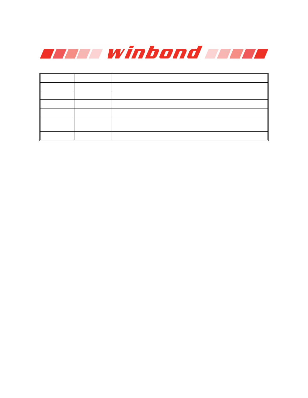
W83697HF
5.9 Power Pins
SYMBOL PIN FUNCTION
VCC 5, 45, 75, +5V power supply for the digital circuitry.
VSB 99 +5V stand-by power supply for the digital circuitry.
VCC3V 22 +3.3V power supply for driving 3V on host interface.
AVCC 105 Analog VCC input. Internally supplier to all analog circuitry.
AGND 112 Internally connected to all analog circuitry. The ground reference for
all analog inputs.
GND 18, 60, 90, Ground.
6. HARDWARE MONITOR
6.1 General Description
The W83697HF can be used to monitor several critical hardware parameters of the system, including
power supply voltages, fan speeds, and temperatures, which are very important for a high-end
computer system to work stable and properly. W83697HF provides LPC interface to access
hardware .An 8-bit analog-to-digital converter (ADC) was built inside W83697HF. The W83697HF can
simultaneously monitor 7 analog voltage inputs, 2 fan tachometer inputs, 2 remote temperature, one
case-open detection signal. The remote temperature sensing can be performed by thermistors, or
2N3904 NPN-type transistors, or directly from Intel
W83697HF provides: 2 PWM (pulse width modulation) outputs for the fan speed control; beep tone
output for warning; SMI#(through serial IRQ), OVT#, GPO# signals for system protection events.
TM
Deschutes CPU thermal diode output. Also the
Through the application software or BIOS, the users can read all the monitored parameters of system
from time to time. And a pop-up warning can be also activated when the monitored item was out of
the proper/preset range. The application software could be Winbond's Hardware Doctor
LDCM (LanDesk Client Management), or other management application software. Also the users can
set up the upper and lower limits (alarm thresholds) of these monitored parameters and to activate
one programmable and maskable interrupts. An optional beep tone could be used as warning signal
when the monitored parameters is out of the preset range.
TM
, or IntelTM
6.2 Access Interface
The W83697HF provides two interface for microprocessor to read/write hardware monitor internal
registers.
6.2.1 LPC interface
The first interface uses LPC Bus to access which the ports of low byte (bit2~bit0) are defined in the
port 5h and 6h. The other higher bits of these ports is set by W83697HF itself. The general decoded
address is set to port 295h and port 296h. These two ports are described as following:
Port 295h: Index port.
Publication Release Date: April 14, 2005
- 19 - Revision2.0
Port 296h: Data port.
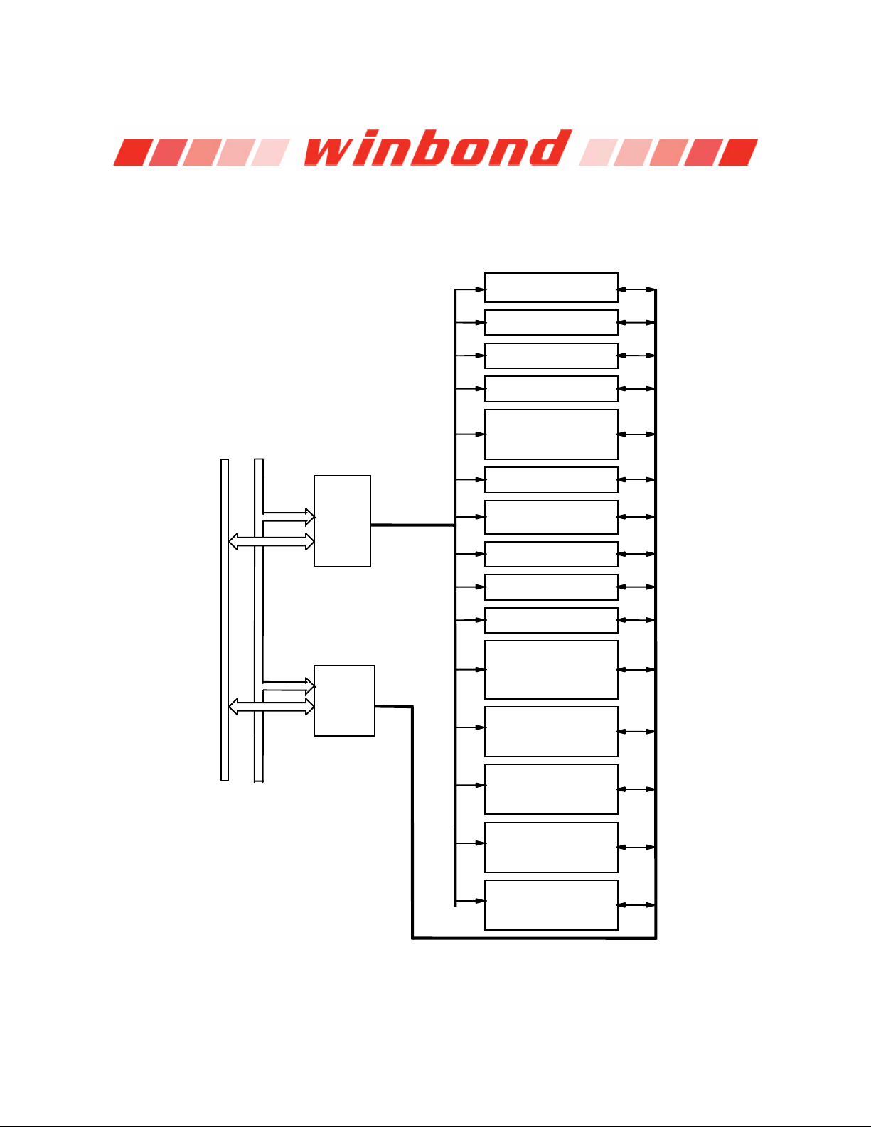
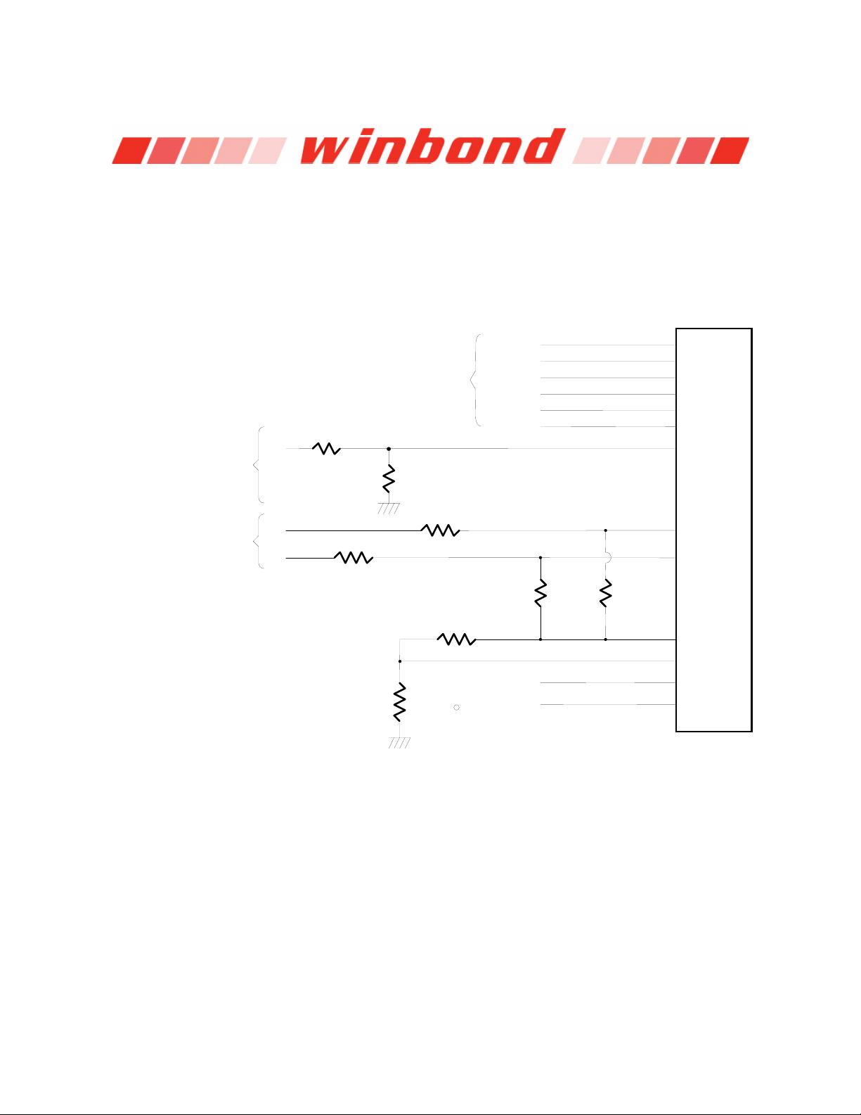
The register structure is showed as the Figure 9.1
ISA
Address
Bus
Port 5h
Index
Register
Port 6h
Data
Register
ISA
Data
Bus
Configuration Register
40h
SMI# Status/Mask Registers
41h, 42h, 44h, 45h
Fan Divisor Register
Temperature 2, 3 Serial
Bus Address
Select Bank for 50h~5Fh Reg.
Temperature 2 Control/Staus
Registers
47h
Device ID
48h
Monitor Value Registers
20h~3Fh
and
60h~7Fh (auto-increment)
VID<4>/Device ID
49h
4Ah
Control Register
4Bh~4Dh
4Eh
Winbond Vendor ID
4Fh
BANK 0
R-T Table Value
BEEP Control Register
Winbond Test Register
50h~58h
BANK 1
50h~56h
W83697HF
BANK 2
Reserved
50h~56h
BANK 4
Additional Control/Staus
Registers
50h~5Ch
BANK 5
Additional Limit Value &
Value RAM
50h~57h
Figure 9.1 : ISA interface access diagram
- 20 -
W83697HF
6.3 Analog Inputs
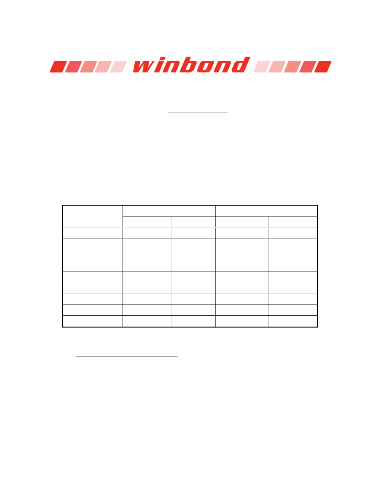
The maximum input voltage of the analog pin is 4.096V because the 8-bit ADC has a 16mv LSB.
Really, the application of the PC monitoring would most often be connected to power suppliers. The
CPU V-core voltage, +3.3V, battery and 5VSB voltage can directly connected to these analog inputs.
The +12V,-12V and -5V voltage inputs should be reduced a factor with external resistors so as to
obtain the input range. As Figure 9.2 shows.
VCOREA
VCOREB
+3.3VIN
AVCC(+5V)
VBAT
5VSB
Positive Input
Positive Inputs
V1
R1
+12VIN
R2
Pin 100
Pin 99
Pin 98
Pin 97
Pin 74
Pin 61
Pin 96
8-bit ADC
with
16mV LSB
Negative Input
Typical Thermister Connection
V2
V3
R3
R5
R
10K, 1%
R
THM
10K, 25 C
**The Connections of VTIN1 and VTIN2
VREF Pin 101
VTIN3
VTIN2
VTIN1
are same as VTIN3
N12VIN
N5VIN
R6
Pin 102
Pin 103
Pin 104
Pin 95
Pin 94
R4
Publication Release Date: April 14, 2005
- 21 - Revision2.0

6.3.1 Monitor over 4.096V voltage
R
K
Ω
Ω
−
×
β
The input voltage +12VIN can be expressed as following equation.
W83697HF
12
VIN V
=×
1
The value of R1 and R2 can be selected to 28K Ohms and 10K Ohms, respectively, when the input
voltage V1 is 12V. The node voltage of +12VIN can be subject to less than 4.096V for the maximun
input range of the 8-bit ADC. The Pin 97 is connected to the power supply VCC with +5V. There are
two functions in this pin with 5V. The first function is to supply internal analog power in the W83697HF
and the second function is that this voltage with 5V is connected to internal serial resistors to monitor
the +5V voltage. The value of two serial resistors are 34K ohms and 50K ohms so that input voltage to
ADC is 2.98V which is less than 4.096V of ADC maximum input voltage. The express equation can
represent as follows.
VVCC
=×
in
where VCC is set to 5V.
The Pin 61 is connected to 5VSB voltage. W83697HF monitors this voltage and the internal two serial
resistors are 17K Ω and 33K Ω so that input voltage to ADC is 3.3V which less than 4.096V of ADC
maximum input voltage.
6.3.2 Monitor negative voltage
The negative voltage should be connected two series resistors and a positive voltage VREF (is equal
to 3.6V). In the Figure 9.2, the voltage V2 and V3 are two negative voltage which they are -12V and 5V respectively. The voltage V2 is connected to two serial resistors then is connected to another
terminal VREF which is positive voltage. So as that the voltage node N12VIN can be obtain a posedge
voltage if the scales of the two serial resirtors are carefully selected. It is recommanded from Winbond
that the scale of two serial resistors are R3=232K ohms and R4=56K ohm. The input voltage of node
N12VIN can be calculated by following equation.
50
KK
50 34
ΩΩ
2
RR
+
12
+
≅
298
.
V
K
N VIN VREF V
If the V2 is equal to -12V then the voltage is equal to 0.567V and the converted hexdecimal data is set
to 35h by the 8-bit ADC with 16mV-LSB.This monitored value should be converted to the real negative
votage and the express equation is shown as follows.
Where β is 232K/(232K+56K). If the N2VIN is 0.567 then the V2 is approximately equal to -12V.
=+×
where VREF is equal 3.6V.
=
V
2
22
N VIN VREF
12
1
- 22 -
232
KK
232 56
−
β
+
ΩΩ
V12
+()( )
W83697HF
−
×
γ
The another negative voltage input V3 (approximate -5V) also can be evaluated by the similar method
and the serial resistors can be selected with R5=120K ohms and R6=56K ohms by the Winbond
recommended. The expression equation of V3 With -5V voltage is shown as follows.
N VIN VREF
5
=
V
3
Where the γ is set to 120K/(120K+56K). If the monitored ADC value in the N5VIN channel is 0.8635,
VREF=3.6V and the parameter γ is 0.6818 then the negative voltage of V3 can be evalated to be -5V.
1
−
γ
6.3.3 Temperature Measurement Machine
The temperature data format is 8-bit two's-complement for sensor 2 and 9-bit two's-complement for
sensor 1. The 8-bit temperature data can be obtained by reading the CR[27h]. The 9-bit temperature
data can be obtained by reading the 8 MSBs from the Bank1 CR[50h] and the LSB from the Bank1
CR[51h] bit 7. The format of the temperature data is show in Table 1.
Temperature 8-Bit Digital Output 9-Bit Digital Output
+125°C 0111,1101 7Dh 0,1111,1010 0FAh
+25°C 0001,1001 19h 0,0011,0010 032h
+1°C 0000,0001 01h 0,0000,0010 002h
+0.5°C - - 0,0000,0001 001h
+0°C 0000,0000 00h 0,0000,0000 000h
-0.5°C - - 1,1111,1111 1FFh
-1°C 1111,1111 FFh 1,1111,1110 1FFh
-25°C 1110,0111 E7h 1,1100,1110 1CEh
-55°C 1100,1001 C9h 1,1001,0010 192h
6.3.3.1 Monitor temperature from thermistor: The W83697HF can connect three thermistors to measure three different envirment temperature. The
specification of thermistor should be considered to (1) β value is 3435K, (2) resistor value is 10K ohms
at 25°C. In the Figure 9.2, the themistor is connected by a serial resistor with 10K Ohms, then connect
to VREF (Pin 101).
6.3.3.2 Monitor temperature from Pentium II
The W83697HF can alternate the thermistor to Pentium II
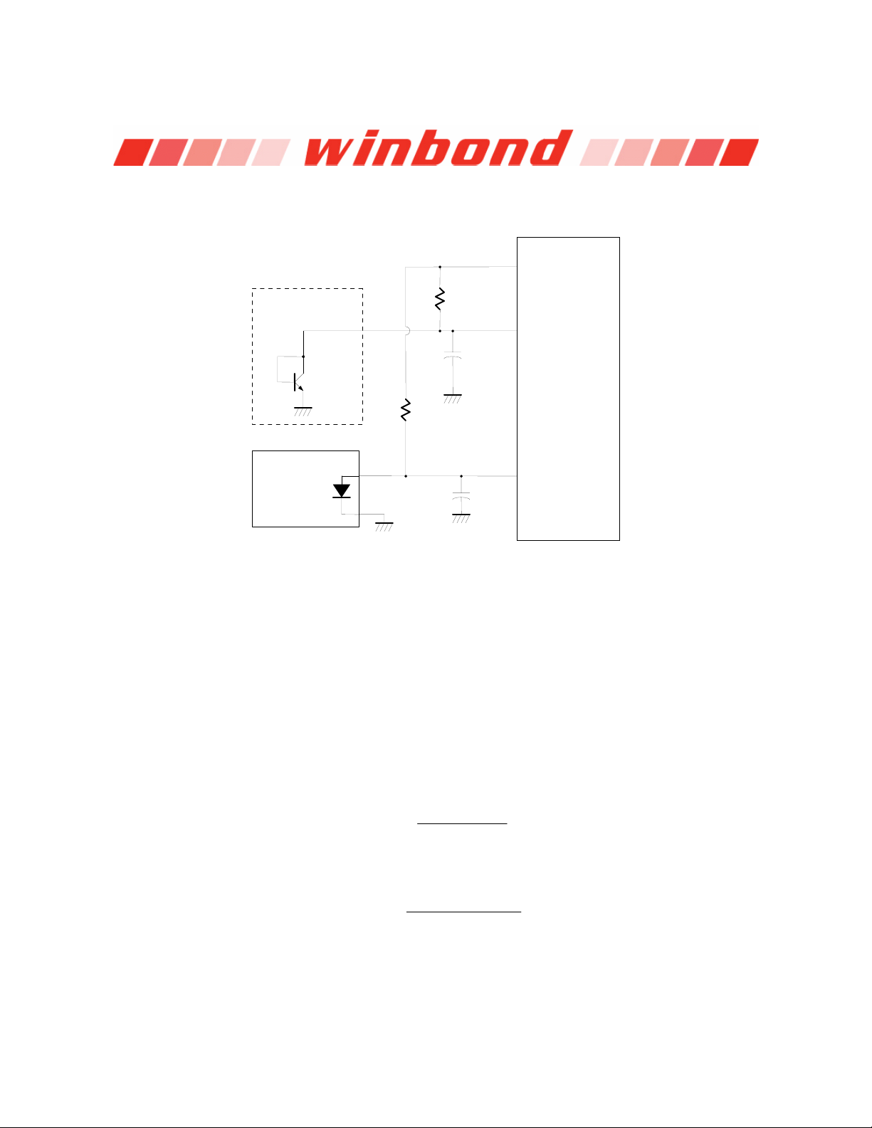
transistor 2N3904 and the circuit connection is shown as Figure 9.3. The pin of Pentium II
connected to power supply ground (GND) and the pin D+ is connected to pin VTINx in the
W83697HF. The resistor R=30K ohms should be connected to VREF to supply the diode bias current
8-Bit Binary 8-Bit Hex 9-Bit Binary 9-Bit Hex
Table 2.
TM
thermal diode or bipolar transistor 2N3904
TM
(Deschutes) thermal diode interface or
TM
D- is
Publication Release Date: April 14, 2005
- 23 - Revision2.0
W83697HF
and the bypass capacitor C=3300pF should be added to filter the high frequency noise. The transistor
2N3904 should be connected to a form with a diode, that is, the Base (B) and Collector (C) in the
2N3904 should be tied togeter to act as a thermal diode.
VREF
Bipolar Transistor
Temperature Sensor
C
B
2N3904
E
OR
Pentium II
CPU D+
Therminal
Diode
D-
R=30K, 1%
VTINx
C=3300pF
W83627HF
R=30K, 1%
VTINx
C=3300pF
Figure 9.3
6.4 FAN Speed Count and FAN Speed Control
6.4.1 Fan Speed Count
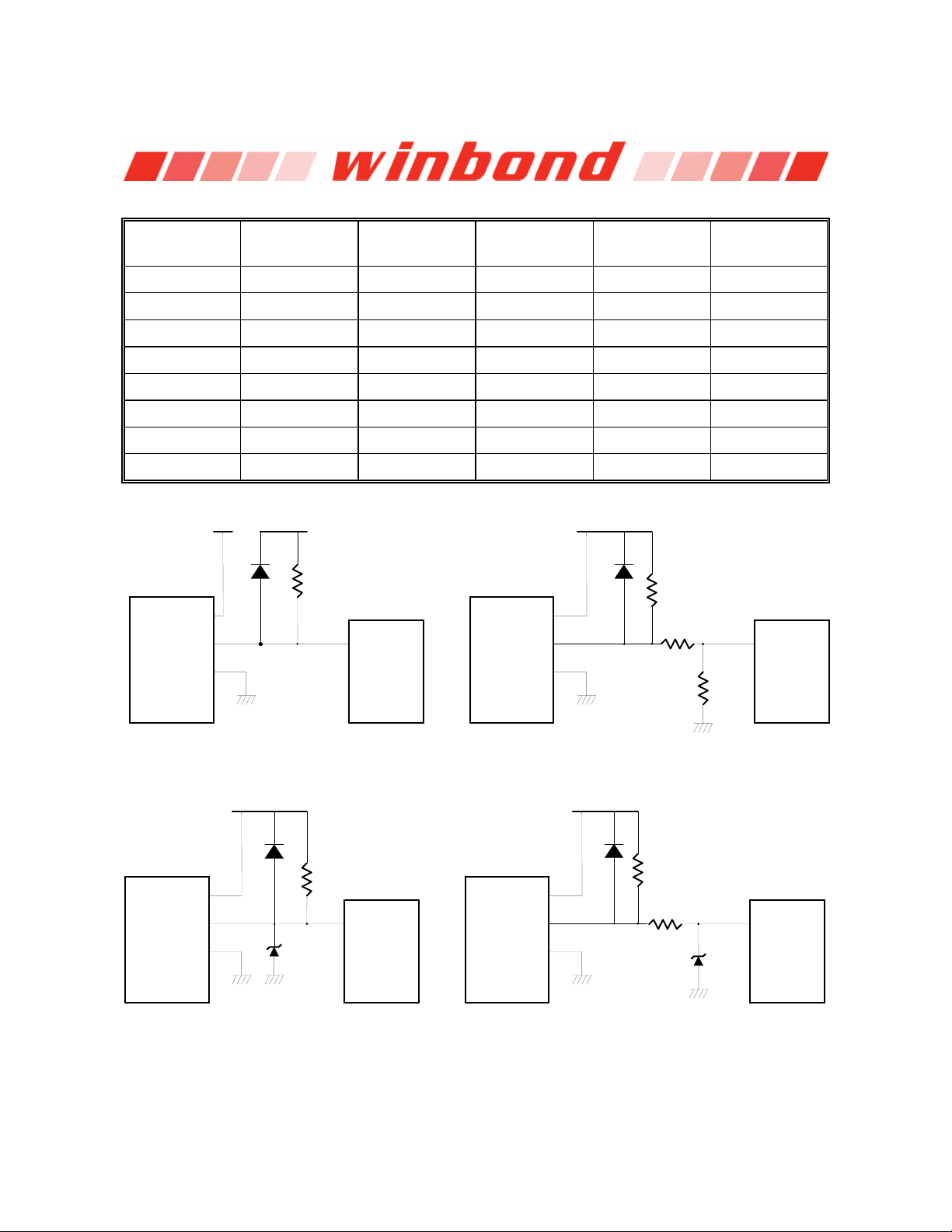
Inputs are provides for signals from fans equipped with tachometer outputs. The level of these signals
should be set to TTL level, and maximum input voltage can not be over +5.5V. If the input signals from
the tachometer outputs are over the VCC, the external trimming circuit should be added to reduce the
voltage to obtain the input specification. The normal circuit and trimming circuits are shown as Figure
9.4.
Determine the fan counter according to:
.
Count
135 10
=
RPM Divisor
In other words, the fan speed counter has been read from register CR28 or CR29 or CR2A, the fan
speed can be evaluated by the following equation.
135 10
RPM
=
.
Count Divisor
The default divisor is 2 and defined at CR47.bit7~4, CR4B.bit7~6, and Bank0 CR5D.bit5~7 which are
three bits for divisor. That provides very low speed fan counter such as power supply fan. The
followed table is an example for the relation of divisor, PRM, and count.
6
×
×
×
×
6
- 24 -
W83697HF
Divisor
Nominal
PRM
Time per
Revolution
Counts 70% RPM Time for 70%
1 8800 6.82 ms 153 6160 9.74 ms
2 (default)
4400 13.64 ms
153
3080 19.48 ms
4 2200 27.27 ms 153 1540 38.96 ms
8 1100 54.54 ms 153 770 77.92 ms
16 550 109.08 ms 153 385 155.84 ms
32 275 218.16 ms 153 192 311.68 ms
64 137 436.32 ms 153 96 623.36 ms
128 68 872.64 ms 153 48 1246.72 ms
Table 1.
+12V
+12V
FAN Out
GND
FAN
Connector
+5V
Pull-up resister
diode diode
4.7K Ohms
Fan Input
Pin 111-113
W83627HF
FAN
Connector
+12V
FAN Out
GND
+12V
Pull-up resister
4.7K Ohms
14K~39K
Fan Input
10K
Pin 111-113
W83627HF
Fan with Tach Pull-Up to +5V
Fan with Tach Pull-Up to +12V, or Totem-Pole
Output and Register Attenuator
+12V
+12V
FAN Out
GND
FAN
Connector
diode
Fan Input
3.9V Zener
Pull-up resister
> 1K
Pin 111-113
W83627HF
Fan with Tach Pull-Up to +12V and Zener Clamp
Connector
Fan with Tach Pull-Up to +12V, or Totem-Pole
Output and Zener Clamp
FAN Out
FAN
+12V
GND
+12V
diode
> 1K
3.9V Zener
Pull-up resister < 1K
or totem-pole output
Fan Input
Pin 111-113
W83627HF
Figure 9.4
Publication Release Date: April 14, 2005
- 25 - Revision2.0
W83697HF
d
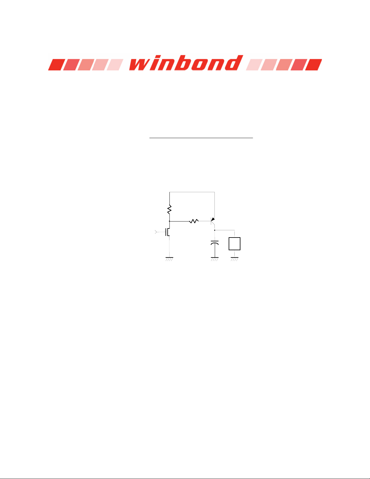
6.4.2 Fan Speed Control
The W83697HF provides 2 sets for fan PWM speed control. The duty cycle of PWM can be
programmed by a 8-bit registers which are defined in the Bank0 CR5A and CR5B. The default duty
cycle is set to 100%, that is, the default 8-bit registers is set to FFh. The expression of duty can be
represented as follows.
−= ×(%) 100%
Duty cycle
Programme
8-bit Register Value
255
The PWM clock frequency also can be program and defined in the Bank0.CR5C . The application
circuit is shown as follows.
+12V
R1
PWM Clock Input
D
G
NMOS
S
Figure 9.5
R2
PNP Transistor
+
C
-
FAN
- 26 -
6.5 SMI# Interrupt Mode
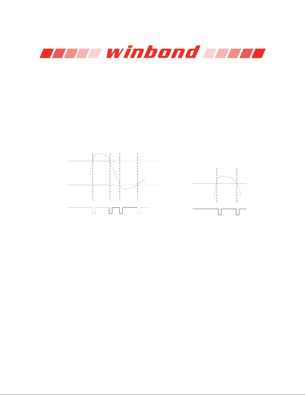
6.5.1 Voltage SMI# mode
SMI# interrupt for voltage is Two-Times Interrupt Mode. Voltage exceeding high limit or going
below low limit will causes an interrupt if the previous interrupt has been reset by reading all
the interrupt Status Register. (Figure 9.6)
6.5.2 Fan SMI# mode
SMI# interrupt for fan is Two-Times Interrupt Mode. Fan count exceeding the limit, or
exceeding and then going below the limit, will causes an interrupt if the previous interrupt has
been reset by reading all the interrupt Status Register. (Figure 9.7)
High limit
W83697HF
Low limit
SMI#
***
*Interrupt Reset when Interrupt Status Registers are read
*
Fan Count limit
SMI#
*
*
Figure 9.6 Figure 9.7
6.5.3 The W83697HF temperature sensor 1 SMI# interrupt has two modes
(1) Comparator Interrupt Mode
Setting the T
the Comparator Interrupt Mode. Temperature exceeds T
(Temperature Hysteresis) limit to 127°C will set temperature sensor 1 SMI# to
HYST
(Over Temperature) Limit causes an
O
interrupt and this interrupt will be reset by reading all the Interrupt Status Register. Once an
interrupt event has occurred by exceeding T
, the interrupt will occur again when the next conversion has completed. If an interrupt event
T
O
has occurred by exceeding T
and not reset, the interrupts will not occur again. The interrupts
O
will continue to occur in this manner until the temperature goes below T
, then reset, if the temperature remains above the
O
. (Figure 9.8)
O
(2) Two-Times Interrupt Mode
Setting the T
Mode. Temperature exceeding T
lower than TO will set temperature sensor 1 SMI# to the Two-Times Interrupt
HYST
causes an interrupt and then temperature going below T
O
will also cause an interrupt if the previous interrupt has been reset by reading all the interrupt
Status Register. Once an interrupt event has occurred by exceeding T
temperature remains above the T
, the interrupt will not occur. (Figure 9.9)
HYST
, then reset, if the
O
HYST
Publication Release Date: April 14, 2005
- 27 - Revision2.0
 Loading...