


查询W83627SF供应商
W83627SF
WINBOND I/O
W83627SF Data Sheet Revision History
Pages Dates Version Version
on Web
1 n.a. 2000/09/17 0.50 First published
2 All 2000/11/15 0.60 New composition
3
4
5
6
7
8
9
10
Main Contents
Please note that all data and specifications are subject to change without notice. All the
trade marks of products and companies mentioned in this data sheet belong to their
respective owners.
LIFE SUPPORT APPLICATIONS
These products are not designed for use in life support appliances, devices, or systems
where malfunction of these products can reasonably be expected to result in personal
injury. Winbond customers using or selling these products for use in such applications
do so at their own risk and agree to fully ind emnify Winbond for any damages resulting
from such improper use or sales.

W83627SF
P R E L I M I N A R Y
TABLE OF CONTENTS
GENERAL DESCRIPTION ---------------------------------------------------------------------------------- 1
PIN CONFIGURATION FOR W83627SF---------------------------------------------------------------- 6
1. PIN DESCRIPTION------------------------------------------------------------------------------------------------------------------------- 7
1.1 LPC INTERFACE -------------------------------------------------------------------------------------------------------------------------- 7
1.2 FDC INTERFACE-------------------------------------------------------------------------------------------------------------------------- 8
1.3 MULTI-MODE PARALLEL PORT ---------------------------------------------------------------------------------------------------- 9
1.4 SERIAL PORT INTE RFACE------------------------------------------------------------------------------------------------------------ 13
1.5 KBC INTERFACE-------------------------------------------------------------------------------------------------------------------------- 15
1.6 ACPI INTERFACE------------------------------------------------------------------------------------------------------------------------- 15
1.7 GAME PORT & MIDI PORT------------------------------------------------------------------------------------------------------------ 16
1.8 GENERAL PURPOSE I/O PORT-------------------------------------------------------------------------------------------------------- 17
1.8.1 General Purpose I/O Port 1 (Power source is Vcc)------------------------------------------------------------------------ 17
1.8.2 General Purpose I/O Port 2 (Power source is Vcc)------------------------------------------------------------------------ 17
1.8.3 General Purpose I/O Port 3 (Power souce is VSB) ------------------------------------------------------------------------ 18
1.9 SMART CARD INTERFACE AND GENERAL PURPOSE I/O PORT 7 (POWERED BY VCC EXCEPT
SCPSNT# WHICH IS POWERED BY VSB)---------------------------------------------------------------------------------------------- 19
1.10 GENERAL PURPOSE I/O PORT 4 (POWERED BY GP4PWR) ---------------------------------------------------------------- 20
1.11 GENERAL PURPOSE I/O PORT 5, 6 (POWERED BY VCC)--------------------------------------------------------------------20
1.12 32KHZ CRYSTAL OSCILLATOR---------------------------------------------------------------------------------------------------- 21
1.13 POWER PINS------------------------------------------------------------------------------------------------------------------------------ 21
2. LPC (LOW PIN COUNT) INTERFACE---------------------------------------------------------------- 22
3. FDC FUNCTIONAL DESCRIPTION ------------------------------------------------------------------ 23
3.1 W83627SF FDC----------------------------------------------------------------------------------------------------------------------------- 23
3.1.1 AT interface--------------------------------------------------------------------------------------------------------------------------- 23
3.1.2 FIFO (Data) -------------------------------------------------------------------------------------------------------------------------- 23
3.1.3 Data Separator---------------------------------------------------------------------------------------------------------------------- 24
Publication Release Date: Nov. 2000
-I - Preliminary Revision 0.60

W83627SF
P R E L I M I N A R Y
3.1.4 Write Precompensation------------------------------------------------------------------------------------------------------------ 25
3.1.5 Perpendicular Recording Mode ------------------------------------------------------------------------------------------------ 25
3.1.6 FDC Core ----------------------------------------------------------------------------------------------------------------------------- 25
3.1.7 FDC Commands--------------------------------------------------------------------------------------------------------------------- 25
3.2 REGISTER DESCRIPTIONS------------------------------------------------------------------------------------------------------------- 36
3.2.1 Status Register A (SA Register) (Read base address + 0) --------------------------------------------------------------- 36
3.2.2 Status Register B (SB Register) (Read base address + 1) --------------------------------------------------------------- 38
3.2.3 Digital Output Register (DO Register) (Write base address + 2) ----------------------------------------------------- 40
3.2.4 Tape Drive Register (TD Register) (Read base address + 3) ----------------------------------------------------------- 40
3.2.5 Main Status Register (MS Register) (Read base address + 4) --------------------------------------------------------- 41
3.2.6 Data Rate Register (DR Register) (Write base address + 4)------------------------------------------------------------ 41
3.2.7 FIFO Register (R/W base address + 5)---------------------------------------------------------------------------------------- 43
3.2.8 Digital Input Register (DI Register) (Read base address + 7) --------------------------------------------------------- 45
3.2.9 Configuration Control Register (CC Register) (Write base address + 7) ------------------------------------------ 46
4. UART PORT--------------------------------------------------------------------------------------------------- 47
4.1 UNIVERSAL ASYNCHRONOUS RECEIVER/TRAN SMITTER (UART A, UART B)------------------------------------ 47
4.2 REGISTER ADDRESS -------------------------------------------------------------------------------------------------------------------- 47
4.2.1 UART Control Register (UCR) (Read/Write)-------------------------------------------------------------------------------- 47
4.2.2 UART Status Register (USR) (Read/Write) ---------------------------------------------------------------------------------- 50
4.2.3 Handshake Control Register (HCR) (Read/Write) ------------------------------------------------------------------------ 51
4.2.4 Handshake Status Register (HSR) (Read/Write)--------------------------------------------------------------------------- 52
4.2.5 UART FIFO Control Register (UFR) (Write only) ------------------------------------------------------------------------- 53
4.2.6 Interrupt Status Register (ISR) (Read only)--------------------------------------------------------------------------------- 54
4.2.7 Interrupt Control Register (ICR) (Read/Write)----------------------------------------------------------------------------- 55
4.2.8 Programmable Baud Generator (BLL/BHL) (Read/Write) -------------------------------------------------------------- 55
4.2.9 User-defined Register (UDR) (Read/Write)---------------------------------------------------------------------------------- 56
5. CIR RECEIVER PORT------------------------------------------------------------------------------------- 57
5.1 CIR REGISTERS---------------------------------------------------------------------------------------------------------------------------- 57
5.1.1 Bank0.Reg0 - Receiver Buffer Registers (RBR) (Read)------------------------------------------------------------------- 57
5.1.2 Bank0.Reg1 - Interrupt Control Register (ICR) ---------------------------------------------------------------------------- 57
5.1.3 Bank0.Reg2 - Interrupt Status Register (ISR)------------------------------------------------------------------------------- 57
5.1.4 Bank0~3.Reg3 - CIR Control Register 0/Bank Select Register (CTR0/BSR) (BANK0~3) --------------------- 58
5.1.5 Bank0.Reg4 - CIR Control Register (CTR) ---------------------------------------------------------------------------------- 58
5.1.6 Bank0.Reg5 - UART Line Status Register (USR) -------------------------------------------------------------------------- 59
5.1.7 Bank0.Reg6 - Remote Infrared Config Register (RIR_CFG) ------------------------------------------------------------ 60
Publication Release Date: Nov. 2000
-II - Revision 0.60

W83627SF
P R E L I M I N A R Y
5.1.8 Bank0.Reg7 - User Defined Register (UDR/AUDR) ----------------------------------------------------------------------- 61
5.1.9 Bank1.Reg0~1 - Baud Rate Divisor Latch (BLL/BHL) ------------------------------------------------------------------- 62
5.1.10 Bank1.Reg2 - Version ID Regiister I (VID)--------------------------------------------------------------------------------- 63
5.1.11 Bank0~3.Reg3 - CIR Control Register 0/Bank Select Register (CTR0/BSR) (BANK0~3)-------------------- 63
5.1.12 Bank1.Reg4 - Timer Low Byte Register (TMRL) -------------------------------------------------------------------------- 63
5.1.13 Bank1.Reg5 - Timer High Byte Register (TMRH) ------------------------------------------------------------------------ 63
6. PARALLEL PORT ------------------------------------------------------------------------------------------ 64
6.1 PRINTER INTERFAC E LOGIC--------------------------------------------------------------------------------------------------------- 64
6.2 ENHANCED PARALLEL PORT (EPP) ----------------------------------------------------------------------------------------------- 65
6.2.1 Data Swapper------------------------------------------------------------------------------------------------------------------------ 66
6.2.2 Printer Status Buffer---------------------------------------------------------------------------------------------------------------- 66
6.2.3 Printer Control Latch and Printer Control Swapper--------------------------------------------------------------------- 67
6.2.4 EPP Address Port ------------------------------------------------------------------------------------------------------------------- 67
6.2.5 EPP Data Port 0-3------------------------------------------------------------------------------------------------------------------ 68
6.2.6 Bit Map of Parallel Port and EPP Registers -------------------------------------------------------------------------------- 68
6.2.7 EPP Pin Descriptions-------------------------------------------------------------------------------------------------------------- 69
6.2.8 EPP Operation----------------------------------------------------------------------------------------------------------------------- 69
6.3 EXTENDED CAPABIL ITIES PARALLEL (ECP) PORT-------------------------------------------------------------------------- 70
6.3.1 ECP Register and Mode Definitions------------------------------------------------------------------------------------------- 70
6.3.2 Data and ecpAFifo Port----------------------------------------------------------------------------------------------------------- 71
6.3.3 Device Status Register (DSR)---------------------------------------------------------------------------------------------------- 71
6.3.4 Device Control Register (DCR) ------------------------------------------------------------------------------------------------- 72
6.3.5 cFifo (Parallel Port Data FIFO) Mode = 010 ------------------------------------------------------------------------------ 73
6.3.6 ecpDFifo (ECP Data FIFO) Mode = 011 ------------------------------------------------------------------------------------ 73
6.3.7 tFifo (Test FIFO Mode) Mode = 110 ------------------------------------------------------------------------------------------ 73
6.3.8 cnfgA (Configuration Register A) Mode = 111----------------------------------------------------------------------------- 73
6.3.9 cnfgB (Configuration Register B) Mode = 111----------------------------------------------------------------------------- 73
6.3.10 ecr (Extended Control Register) Mode = all------------------------------------------------------------------------------ 74
6.3.11 Bit Map of ECP Port Registers ------------------------------------------------------------------------------------------------ 75
6.3.12 ECP Pin Descriptions------------------------------------------------------------------------------------------------------------ 76
6.3.13 ECP Operation--------------------------------------------------------------------------------------------------------------------- 77
6.3.14 FIFO Operation-------------------------------------------------------------------------------------------------------------------- 77
6.3.15 DMA Transfers --------------------------------------------------------------------------------------------------------------------- 78
6.3.16 Programmed I/O (NON-DMA) Mode----------------------------------------------------------------------------------------- 78
6.4 EXTENSION FDD MO DE (EXTFDD)------------------------------------------------------------------------------------------------ 78
Publication Release Date: Nov. 2000
-III - Revision 0.60

W83627SF
P R E L I M I N A R Y
6.5 EXTENSION 2FDD MODE (EXT2FDD) --------------------------------------------------------------------------------------------- 79
7. KEYBOARD CONTROLLER ----------------------------------------------------------------------------80
7.1 OUTPUT BUFFER------------------------------------------------------------------------------------------------------------------------- 81
7.2 INPUT BUFFER---------------------------------------------------------------------------------------------------------------------------- 81
7.3 STATUS REGISTER ---------------------------------------------------------------------------------------------------------------------- 81
7.4 COMMANDS------------------------------------------------------------------------------------------------------------------------------- 82
7.5 HARDWARE GATEA20/KEYBOARD RESET CONTROL LOGIC------------------------------------------------------------ 84
7.5.1 KB Control Register (Logic Device 5, CR-F0)------------------------------------------------------------------------------ 84
7.5.2 Port 92 Control Register (Default Value = 0x24) ------------------------------------------------------------------------- 84
8. GENERAL PURPOSE I/O ---------------------------------------------------------------------------------85
9. PLUG AND PLAY CONFIGURATION ----------------------------------------------------------------89
9.1 COMPATIBLE PNP----------------------------------------------------------------------------------------------------------------------- 89
9.1.1 Extended Function Registers ---------------------------------------------------------------------------------------------------- 89
9.1.2 Extended Functions Enable Registers (EFERs) ---------------------------------------------------------------------------- 90
9.1.3 Extended Function Index Registers (EFIRs), Extended Function Data Registers(EFDRs) -------------------- 90
9.2 CONFIGURATION SE QUENCE--------------------------------------------------------------------------------------------------------90
9.2.1 Enter the extended function mode---------------------------------------------------------------------------------------------- 90
9.2.2 Configurate the configuration registers-------------------------------------------------------------------------------------- 91
9.2.3 Exit the extended function mode------------------------------------------------------------------------------------------------ 91
9.2.4 Software programming example ------------------------------------------------------------------------------------------------ 91
10. ACPI REGISTERS FEATURES ------------------------------------------------------------------------93
11. SMART CARD INTERFACE--------------------------------------------------------------------------- 94
11.1 RECEIVER BUFFER REGISTER (RBR, READ ONLY AT "BASE ADDRESS + 0" WHEN BDLAB = 0)----------- 94
11.2 TRANSMITTER BUFFER REGISTER (TBR, WRITE ONLY AT "BASE ADDRESS + 0" WHEN BDLAB = 0)-- 94
11.3 INTERRUPT CONTR OL REGISTER (ICR, AT "BASE ADDRESS + 1" WHEN BDLAB = 0)------------------------- 94
11.4 INTERRUPT STATUS REGISTER (ISR, READ ONLY AT "BASE ADDRESS + 2")----------------------------------- 95
11.5 SMART CARD FIFO CONTROL REGISTER (SCFR, WRITE ONLY AT "BASE ADDRESS + 2")----------------- 96
11.6 SMART CARD CONTROL REGISTER (SCCR, WRITE ONLY AT "BASE ADDRESS + 3") -------------------------97
11.7 INTERRUPT ENABLE REGISTER (IER, AT "BASE ADDRESS + 4") ------------------------------------------------------97
11.8 SMART CARD STATUS REGISTER (SCSR, AT "BASE ADDRESS + 5")----------------------------------------------- 98
11.9 EXTENDED CONTROL REGISTER (ECR, AT "BASE ADDRESS + 7")--------------------------------------------------- 99
Publication Release Date: Nov. 2000
-IV - Revision 0.60

W83627SF
P R E L I M I N A R Y
11.10 BAUD RATE DIVISOR LATCH HIGH AND BAUD RATE DIVISOR LAT CH LOW (BHL AND BLL AT
"BASE ADDRESS + 1" AND "BASE ADDRESS + 0" RESPECTIVELY WHE N BDLAB = 1)----------------------------- 100
12. SERIAL IRQ------------------------------------------------------------------------------------------------- 102
12.1 START FRAME-------------------------------------------------------------------------------------------------------------------------- 102
12.2 IRQ/DATA FRAME--------------------------------------------------------------------------------------------------------------------- 102
12.3 STOP FRAME -----------------------------------------------------------------------------------------------------------------------------103
13. CONFIGURATION REGISTER ----------------------------------------------------------------------- 104
13.1 CHIP (GLOBAL) CONTROL REGISTER-------------------------------------------------------------------------------------------- 104
13.2 LOGICAL DEVICE 0 (FDC) ------------------------------------------------------------------------------------------------------------ 110
13.3 LOGICAL DEVICE 1 (PARALLEL PORT)------------------------------------------------------------------------------------------ 114
13.4 LOGICAL DEVICE 2 (UART A)------------------------------------------------------------------------------------------------------ 115
13.5 LOGICAL DEVICE 3 (UART B)------------------------------------------------------------------------------------------------------- 115
13.6 LOGICAL DEVICE 5 (KBC)------------------------------------------------------------------------------------------------------------ 117
13.7 LOGICAL DEVICE 6 (CIR) ------------------------------------------------------------------------------------------------------------- 118
13.8 LOGICAL DEVICE 7 (GAME PORT AND MI DI PORT AND GPIO PORT 1)---------------------------------------------119
13.9 LOGICAL DEVICE 8 (GPIO PORT 2) ------------------------------------------------------------------------------------------------ 120
13.10 LOGICAL DEVICE 9 (GPIO PORT 3,4 AR E POWERED BY STANDBY SOURCE VSB) ------------------------------ 122
13.11 LOGICAL DEVICE A (ACPI)--------------------------------------------------------------------------------------------------------- 123
13.12 LOGICAL DEVICE B (SMART CARD INTERFACE)-------------------------------------------------------------------------- 131
13.13 LOGICAL DEVICE C (GPIO PORT 5,6,7 THIS POWER OF THE PORTS IS SOURCE VCC) ------------------------- 131
14. SPECIFICATIONS ----------------------------------------------------------------------------------------- 134
14.1 ABSOLUTE MAXIMUM RATINGS------------------------------------------------------------------------------------------------ 134
14.2 DC CHARACTERISTICS--------------------------------------------------------------------------------------------------------------- 134
15. APPLICATION CIRCUITS ------------------------------------------------------------------------------137
15.1 PARALLEL PORT E XTENSION FDD-----------------------------------------------------------------------------------------------137
15.2 PARALLEL PORT E XTENSION 2FDD--------------------------------------------------------------------------------------------- 138
15.3 FOUR FDD MODE----------------------------------------------------------------------------------------------------------------------- 138
16. ORDERING INSTRUCTION --------------------------------------------------------------------------- 139
17. HOW TO READ THE TOP MARKING ------------------------------------------------------------- 139
18. PACKAGE DIMENSIONS------------------------------------------------------------------------------- 140
Publication Release Date: Nov. 2000
-V - Revision 0.60

W83627SF
PRELIMINARY
GENERAL DESCRIPTION
The W83627SF is the new generation of Winbond's LPC I/O products. It features a whole new interface,
namely LPC (Low Pin Count) interface, which is supported in mainstream Intel chip-set. This interface
as its name suggests is to provide an economical implementation of I/O's interface with lower pin count
and still maintains equivalent performance as its ISA interface counterpart. Approximately 40 pins are
saved in LPC I/O comparing to ISA implementation. With this additional freedom, we can implement
more devices on a single chip as demonstrated in W83627SF's integration of Game Port and MIDI Port.
It is fully transparent in terms of software which means no BIOS or device driver update is needed except
chip-specific configuration.
As Smart Card application is gaining more and more attention, W83627SF also implements a smart
card reader interface featuring Smart wake-up function. This smart card reader interface fully meets the
ISO7816 and PC/SC (Personal Computer/Smart Card Workgroup) standards. W83627SF provides a
minimum external components and lowest cost soultion for smart card applications.
The disk drive adapter functions of W83627SF include a floppy disk drive controller compatible with the
industry standard 82077/765, data separator, write pre-compensation circuit, decode logic, data rate
selection, clock generator, drive interface control logic, and interrupt and DMA logic. The wide range of
functions integrated onto the W83627SF greatly reduces the number of components required for
interfacing with floppy disk drives. The W83627SF supports four 360K, 720K, 1.2M, 1.44M, or 2.88M
disk drives and data transfer rates of 250 Kb/s, 300 Kb/s, 500 Kb/s,1 Mb/s, and 2 Mb/s.
The W83627SF provides two high-speed serial communication ports (UARTs), one of which supports
serial Infrared communication. Each UART includes a 16-byte send/receive FIFO, a programmable baud
rate generator, complete modem control capability, and a processor interrupt system. Both UARTs
provide legacy speed with baud rate up to 115.2k bps and also advanced speed with baud rates of 230k,
460k, or 921k bps which support higher speed modems. In addition, the W83627SF provides IR
functions: IrDA 1.0 (SIR for 1.152K bps) and TV remote IR (Consumer IR, supporting NEC, RC-5,
extended RC-5, and RECS -80 protocols).
Publication Release Date: Nov. 2000
- 1 - Revision 0.60

W83627SF
PRELIMINARY
The W83627SF supports one PC-compatible printer port (SPP), Bi-directional Printer port (BPP) and
also Enhanced Parallel Port (EPP) and Extended Capabilities Port (ECP). Through the printer port
interface pins, also available are: Extension FDD Mode and Extension 2FDD Mode allowing one or two
external floppy disk drives to be connected.
The configuration registers support mode selection, function enable/disable, and power down function
selection. Furthermore, the configurable PnP features are compatible with the plug-and-play feature
demand of Windows 95/98TM, which makes system resource allocation more efficient than ever.
The W83627SF provides functions that complies with ACPI (Advanced Configuration and Power
Interface), which includes support of legacy and ACPI power management through
function pins. For OnNow keyboard Wake-Up, OnNow mouse Wake-Up, and OnNow CIR Wake-Up.
The W83627SF also has auto power management to reduce the power consumption.
The keyboard controller is based on 8042 compatible instruction set with a 2K Byte programmable ROM
and a 256-Byte RAM bank. Keyboard BIOS firmware are available with optional AMIKEY
MultiKey/42TM, or customer code.
The W83627SF provides a set of flexible I/O control functions to the system designer through a set of
General Purpose I/O ports. These GPIO ports may serve as simple I/O or may be individually configured
to provide a predefined alternate function.
The W83627SF is made to fully comply with Microsoft PC98 and PC99 Hardware Design Guide.
Moreover, W83627SF is made to meet the specification of PC2000/PC2001's requirement in the power
management: ACPI and DPM (Device Power Management).
The W83627SF contains a game port and a MIDI port. The game port is designed to support 2 joysticks
PME#
TM
or PSOUT#
-2, Phoenix
and can be applied to all standard PC game control devices. They are very important for a entertainment
or consumer computer.
Publication Release Date: Nov. 2000
- 2 - Revision 0.60

FEATURES
General
• Meet LPC Spec. 1.01
• Support LDRQ#(LPC DMA), SERIRQ (serial IRQ)
• Compliant with Microsoft PC2000/PC2001 Hardware Design Guide
• Support DPM (Device Power Management), ACPI
• Programmable configuration settings
• Single 24 or 48 MHz clock input
FDC
• Compatible with IBM PC AT disk drive systems
• Variable write pre-compensation with track selectable capability
W83627SF
PRELIMINARY
• Support vertical recording format
• DMA enable logic
• 16-byte data FIFOs
• Support floppy disk drives and tape drives
• Detects all overrun and underrun conditions
• Built-in address mark detection circuit to simplify the read electronics
• FDD anti-virus functions with software write protect and FDD write enable signal (write data
signal was forced to be inactive)
• Support up to four 3.5-inch or 5.25-inch floppy disk drives
• Completely compatible with industry standard 82077
• 360K/720K/1.2M/1.44M/2.88M format; 250K, 300K, 500K, 1M, 2M bps data transfer rate
• Support 3-mode FDD, and its Win95/98 driver
UART
• Two high-speed 16550 compatible UARTs with 16-byte send/receive FIFOs
• MIDI compatible
• Fully programmable serial-interface characteristics:
--- 5, 6, 7 or 8-bit characters
--- Even, odd or no parity bit generation/detection
- 3 - Revision 0.60
Publication Release Date: Nov. 2000

W83627SF
PRELIMINARY
--- 1, 1.5 or 2 stop bits generation
• Internal diagnostic capabilities:
--- Loop-back controls for communicat ions link fault isolation
--- Break, parity, overrun, framing error simulation
• Programmable baud generator allows division of 1.8461 MHz and 24 MHz by 1 to (216-1)
• Maximum baud rate up to 921k bps for 14.769 MHz and 1.5M bps for 24 MHz
Infrared
• Support IrDA version 1.0 SIR protocol with maximum baud rate up to 115.2K bps
• Support SHARP ASK-IR protocol with maximum baud rate up to 57,600 bps
• Support Consumer IR
Parallel Port
• Compatible with IBM parallel port
• Support PS/2 compatible bi-directional parallel port
• Support Enhanced Parallel Port (EPP) − Compatible with IEEE 1284 specification
• Support Extended Capabilities Port (ECP) − Compatible with IEEE 1284 specification
• Extension FDD mode supports disk drive B; and Extension 2FDD mode supports disk drives A
and B through parallel port
• Enhanced printer port back-drive current protection
Keyboard Controller
• 8042 based with optional F/W from AMIKKEYTM-2, Phoenix MultiKey/42
with 2K bytes of programmable ROM, and 256 bytes of RAM
• Asynchronous Access to Two Data Registers and One status Register
• Software compatibility with the 8042
• Support PS/2 mouse
• Support port 92
• Support both interrupt and polling modes
• Fast Gate A20 and Hardware Keyboard Reset
• 8 Bit Timer/ Counter
TM
or customer code
• Support binary and BCD arithmetic
Publication Release Date: Nov. 2000
- 4 - Revision 0.60

W83627SF
PRELIMINARY
• 6 MHz, 8 MHz, 12 MHz, or 16 MHz operating frequency
Game Port
• Support two separate Joysticks
• Support every Joystick two axis (X,Y) and two button (A,B) controllers
MIDI Port
• The baud rate is 31.25 Kbaud
• 16-byte input FIFO
• 16-byte output FIFO
General Purpose I/O Ports
• 40 programmable general purpose I/O ports
• General purpose I/O ports can serve as simple I/O ports, interrupt steering inputs, ,watching
dog timer output, power LED output, infrared I/O pins, KBC control I/O pins, suspend LED
output, RSMRST# signal, PWROK signal, STR(suspend to DRAM) function, VID control
function,
OnNow Functions
• Keyboard Wake-Up by programmable keys
• Mouse Wake-Up by programmable buttons
• CIR Wake-Up by programmable keys
• SMART Card Wake-up by SCPSNT
• On Now Wake-Up from all of the ACPI sleeping states (S1-S5)
Smart Card Reader Interface
• PC/SC T=0, T=1 compliant
• ISO7816 protocol compliant
• With 16-byte send/receive FIFOs
• Programmable baud generat or
Package
• 128-pin PQFP
Publication Release Date: Nov. 2000
- 5 - Revision 0.60
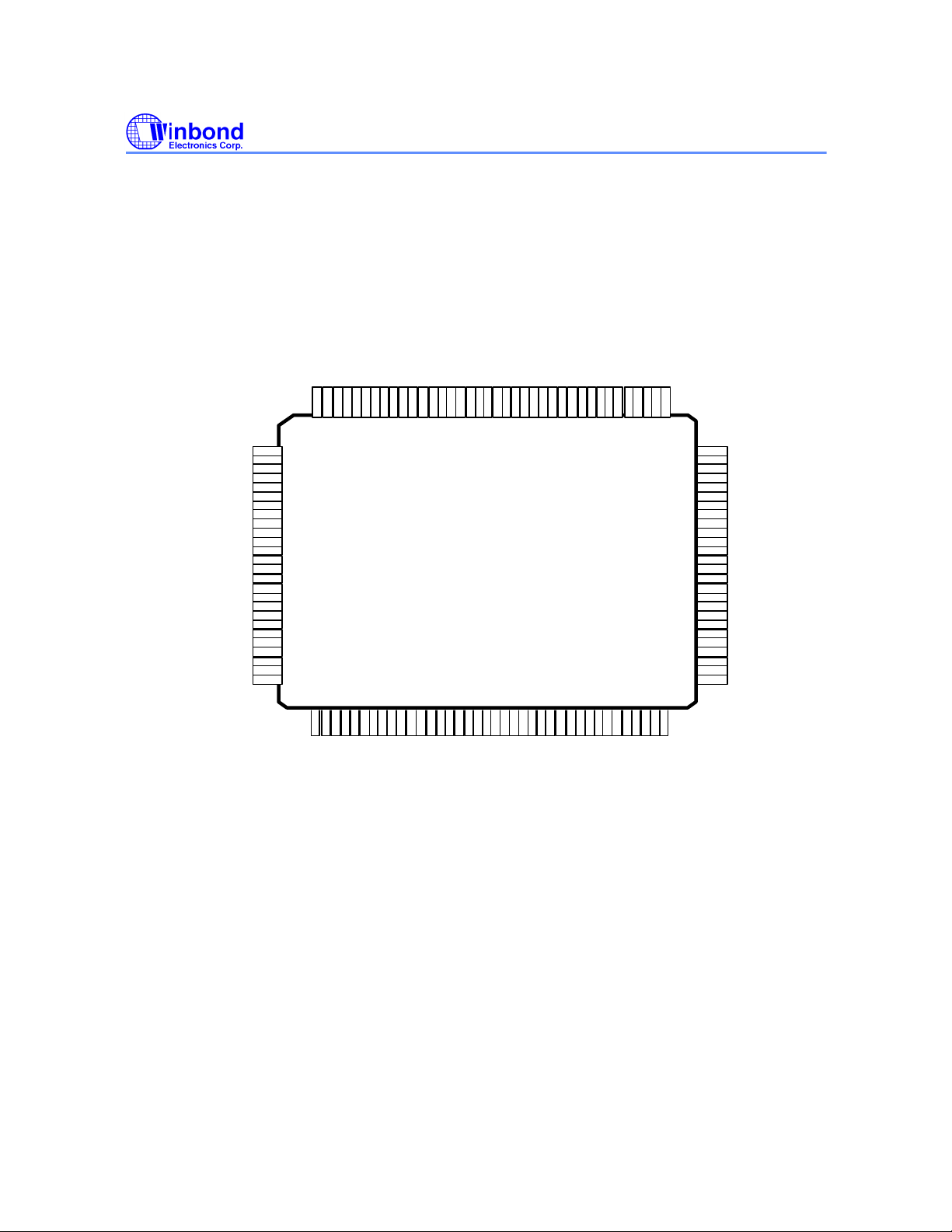
PIN CONFIGURATION FOR W83627SF
GP57CLK/VIDSEL
S5IN#/GP41
STRCTL/GP40
GP56/PVIDLIM1
GP55/VIDO4
GP54/VIDO3
GP53/VIDO2
GP52/VIDO1
GP51/VIDO0
GP50/PVIDLIM0
SCPSNT/GP74
SCIO/GP73
SCPWR/GP72/STGP72
SCRST#/GP70/STGP70
GPY2/P16/GP14
GPX2/P15/GP13
GPX1/P14/GP12
GPSB1/P13/GP11
GPSA1/P12/GP10
VCC
SCCLK/GP71
VSS
MSI/GP20
MSO/IRQIN0
GPSA2/GP17
GPSB2/GP16
GPY1/GP15
GP42/STREN
GP62/VIDI2
GP61/VIDI1
GP60/VIDI0
GP4PWR
1
1
0
0
2
1
103
104
105
106
107
108
109
110
111
112
113
114
115
116
117
118
119
120
121
122
123
124
125
126
127
128
1 2 3 4 5 6 7 8 91011121314151617181920212223242526272829303132333435
32KOUT
XOUT
1
99989796959493929190898887868
0
0
WDTO/GP24
GP22/VID14
GP21/VID13
PLED/GP23
IRRX/GP25
VBAT
XIN
W83627SF
SOUTB/PEN48
IRTX/GP26
DCDB#
RIB#
VSS
8
5
483828180797877
RTSB#/ENGMTO
DSRB#
DTRB#
CTSB#
SINB
VCC
RSMRST#/GP33
PWRCTL#/GP31
SLP_SX#/GP30
PWROK/GP32
VBAT
CIRRX#/GP34
PSOUT#
MDATA
PSIN
36373
SUSCLKIN
GP63
76757473727170696867666
W83627SF
PRELIMINARY
MCLK
5
64
SUSLED/GP35
63
KDATA
62
KCLK
61
VSB
60
KBRST
59
A20GATE
58
KBLOCK#
RIA#
57
56
DCDA#
VSS
55
54
PENKBC/SOUTA
53
SINA
52
PNPCSV#/DTRA#
51
HEFRAS/RTSA#
50
DSRA#
49
CTSA#
48
VCC
47
STB#
46
AFD#
45
ERR#
44
INIT#
43
SLIN#
42
PD0
41
PD1
40
PD2
39
PD3
8
PD4
PD5
PD6
PD7
ACK#
BUSY
PE
SLCT
LRESET#
LFRAME#
VCC3V
LAD0
LAD1
LAD2
LAD3
SERIRQ
LDRQ#
PCICLK
VSS
PME#
CLKIN
DSKCHG#
HEAD#
RDATA#
WP#
TRAKD#
VCC
WE#
WD#
STEP#
DIR#
MOB#
DSA#
DSB#
MOA#
INDEX#
DRVDEN1/IRQIN1/SMI#/GP27
DRVDEN0
Publication Release Date: Nov. 2000
- 6 - Revision 0.60
1. PIN DESCRIPTION
Note: Please refer to Section 13.2 DC CHARACTERISTICS for details.
I/O8t - TTL level bi-directional pin with 8 mA source-sink capability
I/O
- TTL level bi-directional pin with 12 mA source-sink capability
12t
I/O
- 3.3V TTL level bi-directional pin with 12 mA source-sink capability
12tp3
I/OD
- TTL level bi-directional pin open drain output with 12 mA sink capability
12t
I/OD
- TTL level bi-directional pin open drain output with 16 mA sink capability
16t
I/OD24 - TTL level bi-directional pin open drain output with 24A sink capability
OUT2 - Output pin with 2 mA source-sink capability
OUT12 - Output pin with 12 mA source-sink capability
O
- 3.3V output pin with 12 mA source-sink capability
12
tp3
OD12 - Open-drain output pin with 12 mA sink capability
OD24 - Open-drain output pin with 24 mA sink capability
INcs - CMOS level Schmitt-trigger input pin
INt - TTL level input pin
INtd - TTL level input pin with internal pull down resistor
INts - TTL level Schmitt-trigger input pin
IN
- 3.3V TTL level Schmitt-trigger input pin
tsp3
W83627SF
PRELIMINARY
1.1 LPC Interface
SYMBOL PIN I/O FUNCTION
CLKIN 18 INt
PME#
PCICLK 21 IN
LDRQ# 22 O
19 OD12 Generated PME event.
tsp3
12tp3
SERIRQ 23 I/OD12t Serial IRQ input/Output.
LAD[3:0] 24-27 I/O
LFRAME#
LRESET#
29 IN
30 IN
12tp3
tsp3
tsp3
SUSCLKIN 75 INts 32khz clock input , for CIR only.
System clock input. According to the input frequency 24MHz or
48MHz, it is selectable through register. Default is 24MHz input.
PCI clock input.
Encoded DMA Request signal.
These signal lines communicat e address, control, and data
information over the LPC bus between a host and a peripheral.
Indicates start of a new cycle or termination of a broken cycle.
Reset signal. It can connect to PCIRST# signal on the host.
- 7 - Revision 0.60
Publication Release Date: Nov. 2000
1.2 FDC Interface
SYMBOL PIN I/O FUNCTION
DRVDEN0 1 OD24 Drive Density Select bit 0.
DRVDEN1
SMI#
IRQIN1
GP27
2 OD12
OD12
INt
I/OD
12t
Drive Density Select bit 1. (Default)
System Management Interrupt.
Interrupt channel input.
General purpose I/O port 2 bit 7.
W83627SF
PRELIMINARY
INDEX#
MOA#
DSB#
DSA#
MOB#
DIR#
STEP#
WD#
WE#
TRAK0#
3 INcs This Schmitt-triggered input from the disk drive is active low when
the head is positioned over the beginning of a track marked by an
index hole. This input pin is pulled up internally by a 1 KΩ
resistor. The resistor can be disabled by bit 7 of L0-CRF0
(FIPURDWN).
4 OD24 Motor A On. When set to 0, this pin enables disk drive 0. This is
an open drain output.
5 OD24 Drive Select B. When set to 0, this pin enables disk drive B. This
is an open drain output.
6 OD24 Drive Select A. When set to 0, this pin enables disk drive A. This
is an open drain output.
7 OD24 Motor B On. When set to 0, this pin enables disk drive 1. This is
an open drain output.
8 OD24 Direction of the head step motor. An open drain output.
Logic 1 = outward motion
Logic 0 = inward motion
9 OD24 Step output pulses. This active low open drain output produces a
pulse to move the head to another track.
10 OD24 Write data. This logic low open drain writes pre-compensation
serial data to the selected FDD. An open drain output.
11 OD24 Write enable. An open drain output.
13 INcs Track 0. This Schmitt-triggered input from the disk drive is active
low when the head is positioned over the outermost track. This
input pin is pulled up internally by a 1 KΩ resistor. The resistor
can be disabled by bit 7 of L0-CRF0 (FIPURDWN).
Publication Release Date: Nov. 2000
- 8 - Revision 0.60
1.2 FDC Interface, continued
SYMBOL PIN I/O FUNCTION
WP#
14 INcs
Write protected. This active low Schmitt input from the disk drive
indicates that the diskette is write-protected. This input pin is
pulled up internally by a 1 KΩ resistor. The resistor can be
disabled by bit 7 of L0-CRF0 (FIPURDWN).
W83627SF
PRELIMINARY
RDATA#
HEAD#
DSKCHG#
15 INcs The read data input signal from the FDD. This input pin is pulled
up internally by a 1 KΩ resistor. The resistor can be disabled by
bit 7 of L0-CRF0 (FIPURDWN).
16 OD24 Head select. This open drain output determines which disk drive
head is active.
Logic 1 = side 0
Logic 0 = side 1
17 INcs Diskette change. This signal is active low at power on and
whenever the diskette is removed. This input pin is pulled up
internally by a 1 Kresistor. The resistor can be disabled by bit
7 of L0-CRF0 (FIPURDWN).
1.3 Multi-Mode Parallel Port
SYMBOL PIN I/O FUNCTION
SLCT 31 INt
OD12
OD12
PE
OD12
32 INt
OD
PRINTER MODE:
An active high input on this pin indicates that the printer is
selected. Refer to the description of the parallel port for definition
of this pin in ECP and EPP mode.
EXTENSION FDD MODE: WE2#
This pin is for Extension FDD B; its function is the same as the
EXTENSION 2FDD MODE: WD2#
12
pin of FDC.
WE#
EXTENSION 2FDD MODE: WE2#
This pin is for Extension FDD A and B; its function is the same as
the
PRINTER MODE:
An active high input on this pin indicates that the printer has
detected the end of the paper. Refer to the description of the
parallel port for the definition of this pin in ECP and EPP mode.
EXTENSION FDD MODE: WD2#
This pin is for Extension FDD B; its function is the same as the
WD#
This pin is for Extension FDD A and B; its function is the same as
the
pin of FDC.
WE#
pin of FDC.
pin of FDC.
WD#
Publication Release Date: Nov. 2000
- 9 - Revision 0.60

1.3 Multi-Mode Parallel Port, continued
SYMBOL PIN I/O FUNCTION
BUSY 33 INt
OD12
OD
PRINTER MODE:
An active high input indicates that the printer is not ready to
receive data. Refer to the description of the parallel port for
definition of this pin in ECP and EPP mode.
EXTENSION FDD MODE: MOB2#
This pin is for Extension FDD B; its function is the same as the
MOB# pin of FDC.
EXTENSION 2FDD MODE: MOB2#
12
This pin is for Extension FDD A and B; its function is the same as
the MOB# pin of FDC.
ACK# 34 INt
OD12
OD
PRINTER MODE: ACK#
An active low input on this pin indicates that the printer has
received data and is ready to accept more data. Refer to the
description of the parallel port for the definition of this pin in ECP
and EPP mode.
EXTENSION FDD MODE: DSB2#
This pin is for the Extension FDD B; its functions is the same as
the DSB# pin of FDC.
EXTENSION 2FDD MODE: DSB2#
12
This pin is for Extension FDD A and B; its function is the same as
the DSB# pin of FDC.
PD7
35 I/OD
OD12
PRINTER MODE: PD7
12t
Parallel port data bus bit 7. Refer to the description of the parallel
port for the definition of this pin in ECP and EPP mode.
-
EXTENSION FDD MODE: This pin is a tri-state output.
EXTENSION 2FDD MODE : DSA2#
This pin is for Extension FDD A; its function is the same as the
DSA# pin of FDC.
PD6
PD5
36 I/OD
OD12
37 I/O
-
-
-
12t
PRINTER MODE: PD6
12t
Parallel port data bus bit 6. Refer to the description of the parallel
port for the definition of this pin in ECP and EPP mode.
EXTENSION FDD MODE: This pin is a tri-state output.
EXTENSION. 2FDD MODE: MOA2#
This pin is for Extension FDD A; its function is the same as the
MOA# pin of FDC.
PRINTER MODE: PD5
Parallel port data bus bit 5. Refer to the description of the parallel
port for the definition of this pin in ECP and EPP mode.
EXTENSION FDD MODE: This pin is a tri-state output.
EXTENSION 2FDD MODE: This pin is a tri-state output.
W83627SF
PRELIMINARY
Publication Release Date: Nov. 2000
- 10 - Revision 0.60

1.3 Multi-Mode Parallel Port, continued
SYMBOL PIN I/O FUNCTION
PD4
38 I/O
12t
INt
INt
PRINTER MODE: PD4
Parallel port data bus bit 4. Refer to the description of the parallel
port for the definition of this pin in ECP and EPP mode.
EXTENSION FDD MODE: DSKCHG2#
This pin is for Extension FDD B; the function of this pin is the
same as the DSKCHG# pin of FDC. It is pulled high internally.
EXTENSION 2FDD MODE: DSKCHG2#
This pin is for Extension FDD A and B; this function of this pin is
the same as the DSKCHG# pin of FDC. It is pulled high internally.
PD3
39 I/O
12t
INt
INt
PRINTER MODE: PD3
Parallel port data bus bit 3. Refer to the description of the parallel
port for the definition of this pin in ECP and EPP mode.
EXTENSION FDD MODE: RDATA2#
This pin is for Extension FDD B; its function is the same as the
RDATA# pin of FDC. It is pulled high internally.
EXTENSION 2FDD MODE: RDATA2#
This pin is for Extension FDD A and B; its function is the same as
the RDATA# pin of FDC. It is pulled high internally.
PD2
40 I/O
12t
INt
INt
PRINTER MODE: PD2
Parallel port data bus bit 2. Refer to the description of the parallel
port for the definition of this pin in ECP and EPP mode.
EXTENSION FDD MODE: WP2#
This pin is for Extension FDD B; its function is the same as the
WP# pin of FDC. It is pulled high internally.
EXTENSION. 2FDD MODE: WP2#
This pin is for Extension FDD A and B; its function is the same as
the WP# pin of FDC. It is pulled high internally.
PD1
41 I/O
12t
INt
INt
PRINTER MODE: PD1
Parallel port data bus bit 1. Refer to the description of the parallel
port for the definition of this pin in ECP and EPP mode.
EXTENSION FDD MODE: TRAK02#
This pin is for Extension FDD B; its function is the same as the
TRAK0# pin of FDC. It is pulled high internally.
EXTENSION. 2FDD MODE: TRAK02#
This pin is for Extension FDD A and B; its function is the same as
the TRAK0# pin of FDC. It is pulled high internally.
W83627SF
PRELIMINARY
Publication Release Date: Nov. 2000
- 11 - Revision 0.60

1.3 Multi-Mode Parallel Port, continued
SYMBOL PIN I/O FUNCTION
PD0
INt
INt EXTENSION 2FDD MODE: INDEX2#
SLIN# 43 OD12
INIT#
ERR#
42 I/O
44 OD12
45
12t
OD12
OD12
OD12
OD12
INt
OD12
OD12
PRINTER MODE: PD0
Parallel port data bus bit 0. Refer to the description of the parallel
port for the definition of this pin in ECP and EPP mode.
EXTENSION FDD MODE: INDEX2#
This pin is for Extension FDD B; its function is the same as the
INDEX# pin of FDC. It is pulled high internally.
This pin is for Extension FDD A and B; its function is the same as
the INDEX# pin of FDC. It is pulled high internally.
PRINTER MODE: SLIN#
Output line for detection of printer selection. Refer to the
description of the parallel port for the definition of this pin in ECP
and EPP mode.
EXTENSION FDD MODE: STEP2#
This pin is for Extension FDD B; its function is the same as the
STEP# pin of FDC.
EXTENSION 2FDD MODE: STEP2#
This pin is for Extension FDD A and B; its function is the same as
the STEP# pin of FDC.
PRINTER MODE: INIT#
Output line for the printer initialization. Refer to the description of
the parallel port for the definition of this pin in ECP and EPP mode.
EXTENSION FDD MODE: DIR2#
This pin is for Extension FDD B; its function is the same as the
DIR# pin of FDC.
EXTENSION 2FDD MODE: DIR2#
This pin is for Extension FDD A and B; its function is the same as
the DIR# pin of FDC.
PRINTER MODE: ERR#
An active low input on this pin indicates that the printer has
encountered an error condition. Refer to the description of the
parallel port for the definition of this pin in ECP and EPP mode.
EXTENSION FDD MODE: HEAD2#
This pin is for Extension FDD B; its function is the same as the
HEAD#pin of FDC.
EXTENSION 2FDD MODE: HEAD2#
This pin is for Extension FDD A and B; its function is the same as
the HEAD# pin of FDC.
W83627SF
PRELIMINARY
Publication Release Date: Nov. 2000
- 12 - Revision 0.60
W83627SF
PRELIMINARY
1.3 Multi-Mode Parallel Port, continued
SYMBOL PIN I/O FUNCTION
AFD# 46 OD12
OD12
OD12
STB# 47 OD12 PRINTER MODE: STB#
- EXTENSION FDD MODE: This pin is a tri-state output.
- EXTENSION 2FDD MODE: This pin is a tri-state output.
PRINTER MODE: AFD#
An active low output from this pin causes the printer to auto feed a
line after a line is printed. Refer to the description of the parallel
port for the definition of this pin in ECP and EPP mode.
EXTENSION FDD MODE: DRVDEN0
This pin is for Extension FDD B; its function is the same as the
DRVDEN0 pin of FDC.
EXTENSION 2FDD MODE: DRVDEN0
This pin is for Extension FDD A and B; its function is the same as
the DRVDEN0 pin of FDC.
An active low output is used to latch the parallel data into the
printer. Refer to the description of the parallel port for the definition
of this pin in ECP and EPP mode.
1.4 Serial Port Interface
SYMBOL PIN I/O FUNCTION
CTSA#
CTSB# 78 The function of these pins can be tested by reading bit 4 of the
DSRA#
DSRB#
RTSA#
HEFRAS
49 INt Clear To Send. It is the modem control input.
handshake status register.
50
79
51
During power-on reset, this pin is pulled down internally and is
INt Data Set Ready . An active low signal indicates the modem or data
set is ready to establish a communication link and transfer data to
the UART.
I/O8t UART A Request To Send. An active low signal informs the modem
or data set that the controller is ready to send data.
defined as HEFRAS, which provides the power-on value for CR26 bit
6 (HEFRAS). A 4.7 kΩ is recommended if intends to pull up.
(select 4EH as configuration I/O port ′s address)
Publication Release Date: Nov. 2000
- 13 - Revision 0.60
W83627SF
PRELIMINARY
1.4 Serial Port Interface, continued
SYMBOL PIN I/O FUNCTION
RTSB#
ENGMTO
DTRA#
PNPCSV#
DTRB#
SINA
SINB
SOUTA
PENKBC
SOUTB 83 I/O8t UART B Serial Output.
PEN48 During power-on reset, this pin is pulled down internally and is
80 I/O8t UART B Request To Send. An active low signal informs the modem
or data set that the controller is ready to send data.
Power on setting pin for enabling Watch Dog timer and its
countdown. This pin is pulled down internally and provides the
power-on value for bit 0 of CR30 and a count value of 0x0A for CRF6
in logical device 8. A 4.7 kΩ is recommended if intends to pull up.
52
81
53
82
54
During power-on reset, this pin is pulled down internally and is
I/O8t UART A Data Terminal Ready. An active low signal informs the
modem or data set that the controller is ready to communicate.
During power-on reset, this pin is pulled down internally and is
defined as
bit 0 (
(clear the default value of FDC, UARTs, PRT, Game port and MIDI
port)
I/O8t UART B Data Terminal Ready. An active low signal informs the
modem or data set that controller is ready to communicate.
INt Serial Input. It is used to receive serial data through the
communication link.
I/O8t UART A Serial Output. It is used to transmit serial data out to the
communication link.
defined as PENKBC, which provides the power-on value for CR24 bit
2 (ENKBC). A 4.7 kΩ resistor is recommended if intends to pull up.
(enable KBC)
defined as PEN48, which provides the power-on value for CR24 bit 6
(EN48). A 4.7 kΩ resistor is recommended if intends to pull up.
PNPCSV#
PNPCSV#
, which provides the power-on value for CR24
). A 4.7 kΩ is recommended if intends to pull up.
DCDA#
DCDB#
RIA#
RIB#
56
84
57
85
INt Data Carrier Detect. An active low signal indicates the modem or
data set has detected a data carrier.
INt Ring Indicator. An active low signal indicates that a ring signal is
being received from the modem or data set.
Publication Release Date: Nov. 2000
- 14 - Revision 0.60
W83627SF
PRELIMINARY
1.5 KBC Interface
SYMBOL PIN I/O FUNCTION
KBLOCK# 58 INt Keyboard inhibit control input. This pin is after system reset.
Internal pull high. (KBC P17)
A20GATE 59 OUT12 Gate A20 output. This pin is high after system reset. (KBC P21)
KBRST 60 OUT12 Keyboard reset. This pin is high after system reset. (KBC P20)
KCLK 62 I/OD
KDATA 63 I/OD
MCLK 65 I/OD
MDATA 66 I/OD
1.6 ACPI Interface
SYMBOL PIN I/O FUNCTION
PSOUT# 67 OD12 Panel Switch Output. This signal is used for Wake-Up system
PSIN 68 INtd Panel Switch Input. This pin is high active with an internal pull
VBAT 74 PWR Battery voltage input.
Keyboard Clock.
16t
Keyboard Data.
16t
PS2 Mouse Clock.
16t
PS2 Mouse Data.
16t
from S5
down resistor.
state. This pin is pulse output, active low.
cold
Publication Release Date: Nov. 2000
- 15 - Revision 0.60
1.7 Game Port & MIDI Port
SYMBOL PIN I/O FUNCTION
MSI 119 INt MIDI serial data input.
W83627SF
PRELIMINARY
GP20 I/OD
MSO
IRQIN0
GPSA2 121 INcs Active-low, Joystick I switch input 2. This pin has an internal pull-
GP17 I/OD
GPSB2 122 INcs Active-low, Joystick II switch input 2. This pin has an internal pull-
GP16 I/OD12 General purpose I/O port 1 bit 6.
GPY1 123 I/OD12 Joystick I timer pin. this pin connect to Y positioning variable
GP15 I/OD12t General purpose I/O port 1 bit 5.
GPY2
GP14
P16
GPX2
GP13
P15
120 OUT 12
124 I/OD12
I/OD
I/OD12t
125 I/OD12
I/OD
I/OD12t
General purpose I/O port 2 bit 0.
12t
MIDI serial data output. (Default)
INt
Alternate Function input: Interrupt channel input.
up resistor. (Default)
General purpose I/O port 1 bit 7.
12t
up resistor. (Default)
resistors for the Josystick. (Default)
Joystick II timer pin. this pin connect to Y positioning variable
resistors for the Josystick. (Default)
General purpose I/O port 1 bit 4.
12t
Alternate Function Output:KBC P16 I/O port.
Joystick II timer pin. this pin connect to X positioning variable
resistors for the Josystick. (Default)
General purpose I/O port 1 bit 3.
12t
Alternate Function Output:KBC P15 I/O port.
Publication Release Date: Nov. 2000
- 16 - Revision 0.60

1.7 Game Port & MIDI Port, continued
SYMBOL PIN I/O FUNCTION
GPX1
GP12
P14
126 I/OD12
I/OD
12t
I/OD12t
Joystick I timer pin. this pin connect to X positioning variable
resistors for the Josystick. (Default)
General purpose I/O port 1 bit 2.
Alternate Function Output:KBC P14 I/O port.
W83627SF
PRELIMINARY
GPSB1
GP11
P13
GPSA1
GP10
P12
127 INcs
I/OD
12t
I/OD12t
128 INcs
I/OD
12t
I/OD12t
Active-low, Joystick II switch input 1. (Default)
General purpose I/O port 1 bit 1.
Alternate Function Output:KBC P13 I/O port.
Active-low, Joystick I switch input 1. (Default)
General purpose I/O port 1 bit 0.
Alternate Function Output:KBC P12 I/O port.
1.8 General Purpose I/O Port
1.8.1 General Purpose I/O Port 1 (Power source is Vcc)
see 1.7 Game Port
1.8.2 General Purpose I/O Port 2 (Power source is Vcc)
SYMBOL PIN I/O FUNCTION
GP26
IRTX
GP25
IRRX
87 I/OD
OUT 12
88 I/OD
INts
General purpose I/O port 2 bit 6.
12t
Alternate Function Output: Infrared Transmitter Output. (Default)
General purpose I/O port 2 bit 5.
12t
Alternate Function Input: Infrared Receiver input. (Default)
GP24
WDTO
GP23
PLED
GP22
VIDI4
GP21
VIDI3
89 I/OD
OD12
90 I/OD
OD24
91 I/OD
IN
92 I/OD
IN
General purpose I/O port 2 bit 4.
12t
Watch dog timer output. (Default)
General purpose I/O port 2 bit 3.
24t
Power LED output, this signal is low after system reset. (Default)
General purpose I/O port 2 bit 2.
12t
Alternate VID input bit 4.
t
General purpose I/O port 2 bit 1.
12t
Alternate VID input bit 3.
t
Publication Release Date: Nov. 2000
- 17 - Revision 0.60
1.8.3 General Purpose I/O Port 3 (Power souce is VSB)
SYMBOL PIN I/O FUNCTION
W83627SF
PRELIMINARY
GP35
SUSLED
GP34
CIRRX#
GP33
RSMRST#
GP32
PWROK
GP31
PWRCTL#
GP30
SLP_SX#
64 I/OD
69 I/OD
70 I/OD
71 I/OD
72 I/OD
73 I/OD12t
24t
OD24
12t
OD12
12t
OD12
12t
OD12
12t
OD12
INt
General purpose I/O port 3 bit 5.
Suspend LED output, it can program to flash when suspend state.
This function can work without VCC. (Default)
General purpose I/O port 3 bit 4.
Consumer IR receiving input. This pin can Wake-Up system from
S5
General purpose I/O port 3 bit 3.
This pin generates the RSMRST signal while the VSB come in.
(Default)
General purpose I/O port 3 bit 2.
This pin generates the PWROK signal while the VCC come in.
(Default)
General purpose I/O port 3 bit 1.
This pin generates the PWRCTL# signal while the power failure.
(Default)
General purpose I/O port 3 bit 0.
Chpset suspend C status input.
cold.
(Default)
Publication Release Date: Nov. 2000
- 18 - Revision 0.60
W83627SF
PRELIMINARY
1.9 SMART CARD Interface and General Purpose I/O port 7 (Powered by VCC
except SCPSNT# which is powered by VSB)
SYMBOL PIN I/O FUNCTION
SCPSNT
GP74
SCIO
GP73
SCPWR
GP72
STGP72
SCCLK
GP71
SCRST#
GP70
STGP70
112 INts
I/O
12ts
113 I/O
115 OUT12
116 OUT12
118 OUT12
I/OD
I/O
I/O
I/O
12t
12t
12t
12t
12t
Smart card present detection Schmitt-trigger input.
General purpose I/O port 7 bit 4.
Smart card data I/O channel.
General purpose I/O port 7 bit 3.
Smart card power control.
General purpose I/O port 7 bit 2.
Power on setting pin for selecting functions of GP7. Setting value
is latched on the rising edge of POWEROK. This pin is internally
pulled down during power on, a 4.7 kΩ resistor is recommended if
intends to pull up. Refer to detailed descrption of CR2C bit 6, 5.
Smart card clock output.
General purpose I/O port 7 bit 1.
Smart card reset output.
General purpose I/O port 7 bit 0.
Power on setting pin for selecting functions of GP7. Setting value
is latched on the rising edge of POWEROK. This pin is internally
pulled down during power on, a 4.7 kΩ resistor is recommended if
intends to pull up. Refer to detailed descrption of CR2C bit 6, 5.
Publication Release Date: Nov. 2000
- 19 - Revision 0.60

1.10 General Purpose I/O Port 4 (Powered by GP4PWR)
SYMBOL PIN I/O FUNCTION
GP4PWR 101 PWR
GP42
STREN
GP41
S5IN#
GP40
STRCTL
102 I/O
103 I/O
104 I/O
+5V stand-by power supply dedicated for GP4.
General purpose I/O port 4 bit 2.
12t
Power on setting pin for selecting functions of GP4. Setting value
is latched on the rising edge of RSMRST#. This pin is internally
pulled down during power on, a 4.7 kΩ resistor is recommended if
intends to pull up. Refer to detailed descrption of CR29 bit 0.
General purpose I/O port 4 bit 1.
12t
S5 input signal to indicate in S5 state.
General purpose I/O port 4 bit 0.
12t
For suspend to ram function to control Ram power.
1.11 General Purpose I/O Port 5, 6 (Powered by VCC)
SYMBOL PIN I/O FUNCTION
GP57
VIDSEL
GP56
PVIDLIM1
GP55
VIDO4
97 I/O
105 I/O
106 I/OD
OD12
General purpose I/O port 5 bit 7.
12t
Power on setting pin for selecting VID function. Setting value is
latched on the rising edge of POWEROK. This pin is internally
pulled down during power on, a 4.7 kΩ resistor is recommended if
intends to pull up. Refer to detailed descrption of CR2C bit 7.
General purpose I/O port 5 bit 6.
12t
Power on setting pin for selecting VID guarding function. Setting
value is latched on the rising edge of POWEROK. This pin is
internally pulled down during power on, a 4.7 kΩ resistor is
recommended if intends to pull up. Refer to detailed descrption of
bit 6 of CRFA in logical device C.
General purpose I/O port 5 bit 5.
12t
Alternate VID output bit 4.
W83627SF
PRELIMINARY
GP54
VIDO3
GP53
VIDO2
107 I/OD
OD12
108 I/OD
OD12
General purpose I/O port 5 bit 4.
12t
Alternate VID output bit 3.
General purpose I/O port 5 bit 3.
12t
Alternate VID output bit 2.
- 20 - Revision 0.60
Publication Release Date: Nov. 2000
1.11 General Purpose I/O Port 5, 6 (Powered by VCC), continued
SYMBOL PIN I/O FUNCTION
GP52
VIDO1
109 I/OD
OD12
General purpose I/O port 5 bit 2.
12t
Alternate VID output bit 1.
W83627SF
PRELIMINARY
GP51
VIDO0
GP50
PVIDLIM0
110 I/OD
OD12
111 I/O
General purpose I/O port 5 bit 1.
12t
Alternate VID output bit 0.
General purpose I/O port 5 bit 0.
12t
Power on setting pin for selecting VID guarding function. Setting
value is latched on the rising edge of POWEROK. This pin is
internally pulled down during power on, a 4.7 kΩ resistor is
recommended if intends to pull up. Refer to detailed descrption of
bit 5 of CRFA in logical device C.
GP63 76 I/OD
GP62
VIDI2
GP61
VIDI1
GP60
VIDI0
98 I/OD
99
100
I/OD
I/OD
IN
IN
IN
General purpose I/O port 6 bit 2.
12t
General purpose I/O port 6 bit 2.
12t
Alternate VID input bit 2.
t
General purpose I/O port 6 bit 1.
12t
Alternate VID input bit 1.
t
General purpose I/O port 6 bit 0.
12t
Alternate VID input bit 0.
t
1.12 32KHz crystal oscillator
SYMBOL PIN I/O FUNCTION
XIN
VBAT
93 IN Crystal input
94 PWR Dedicated power supply for oscillator.
XOUT 95 OUT Crystal output
CLK32KOUT
96 OUT
32KHz output clock.
2
1.13 POWER PINS
SYMBOL PIN FUNCTION
VCC3V 28 +3.3V power supply for driving 3V on host interface.
VCC 12, 48, 77, 114 +5V power supply for the digital circuitry.
VSB 61 +5V stand-by power supply for the digital circuitry.
VSS 20, 55, 86, 117 Ground.
Publication Release Date: Nov. 2000
- 21 - Revision 0.60
W83627SF
PRELIMINARY
2. LPC (LOW PIN COUNT) INTERFACE
LPC interface is to replace ISA interface serving as a bus interface between host (chip-set) and
peripheral (Winbond I/O). Data transfer on the LP C bus are serialized over a 4 bit bus. The general
characteristics of the interface implemented in Winbond LPC I/O are:
• One control line, namely LFRAME#, which is used by the host to start or stop transfers. No
peripherals drive this signal.
• The LAD[3:0] bus, which communicates information serially. The information conveyed are cycle
type, cycle direction, chip selection, address, data, and wait states.
• MR (master reset) of Winbond ISA I/O is replaced with a active low reset signal, namely LRESET#, in
Winbond LPC I/O.
• An additional 33 MHz PCI clock is needed in Winbond LPC I/O for synchronization.
• DMA requests are issued through LDRQ#.
• Interrupt requests are issued through SERIRQ.
• Power management events are issued through PME#.
Comparing to its ISA counterpart, LPC implementation saves up to 40 pin counts (see table below) free
for integrating more devices on a single chip.
Winbond I/O Interface pins count
W83977EF D[7:0], SA[15:0], DRQ[3:0], DACK#[3:0], TC, IOR#, IOW#, IOCHRDY, IRQs 49
W83627SF LAD[3:0], LFRAME#, PCICLK, LDRQ#, SERIRQ, PME# 9
save 40
The transition from ISA to LPC is transparent in terms of software which means no BIOS or device driver
update is needed except chip-specific configuration.
Publication Release Date: Nov. 2000
- 22 - Revision 0.60

W83627SF
PRELIMINARY
3. FDC FUNCTIONAL DESCRIPTION
3.1 W83627SF FDC
The floppy disk controller of the W83627SF integrates all of the logic required for floppy disk control. Th e
FDC implements a PC/AT or PS/2 solution. All programmable options default to compatible values. The
FIFO provides better system performance in multi-master systems. The digital data separator supports
up to 2 M bits/sec data rate.
The FDC includes the following blocks: AT interface, Precompensation, Data Rate Selection, Digital
Data Separator, FIFO, and FDC Core.
3.1.1 AT interface
The interface consists of the standard asynchronous signals: RD#, WR#, A0-A3, IRQ, DMA control, and
a data bus. The address lines select between the configuration registers, the FIFO and control/status
registers. This interface can be switched between PC/AT, Model 30, or PS/2 normal modes. The PS/2
register sets are a superset of the registers found in a PC/AT.
3.1.2 FIFO (Data)
The FIFO is 16 bytes in size and has programmable threshold values. All command parameter
information and disk data transfers go through the FIFO. Data transfers are governed by the RQM and
DIO bits in the Main Status Register.
The FIFO defaults to disabled mode after any form of reset. This maintains PC/AT hardware
compatibility. The default values can be changed through the CONFIGURE command. The advantage of
the FIFO is that it allows the system a larger DMA latency without causing disk errors. The following
tables give several examples of the delays with a FIFO. The data are based upon the following formula:
Publication Release Date: Nov. 2000
- 23 - Revision 0.60
 Loading...