

Willsemi WPM3401 Schematic [ru]
WPM3401
WPM3401
P-Channel Enhancement Mode MOSFET
www.willsemi.com
Description
The WPM3401 is the P-Channel logic enhancement mode
power field effect transistors are produced using high cell
density, DMOS trench technology.
This high density process is especially tailored to minimize
on-state resistance. These devices are particularly suited for low
voltage application, notebook computer power management and
other battery powered circuits where high-side switching.
Features
z -30V/-4.3A,RDS(ON) 53m@VGS= -10V
z -30V/-3.4A,RDS(ON) 56m@VGS=-4.5V
z Super high density cell design for extremely low RDS (ON)
z Exceptional on-resistance and maximum DC current
capability
z SOT23-3
package design
<
<
Application
z Power Management in Note book
z Portable Equipment
z Battery Powered System
z DC/DC Converter
z Load Switch
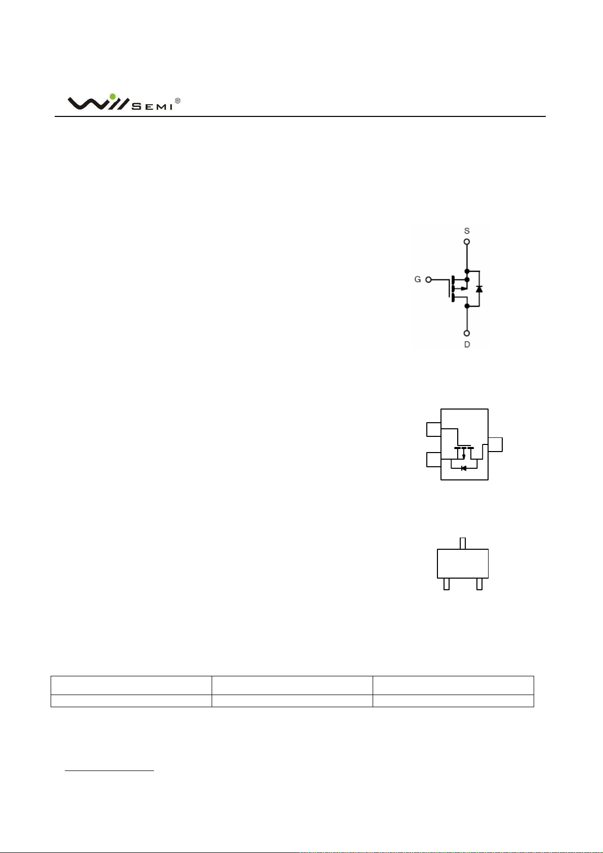
P−Channel MOSFET
G
1
S
2
Top View
Drain
3
WP1U
G
1
Gate Source
= Date Code
U
= Specific Device Code
WP1
D
3
2
Order information
Part Number
WPM3401-3/TR SOT23-3 3000 Tape&Reel
http://www.willsemi.com Page 1
Package
Shipping
Oct,
0 2012 Rev 2.
2
Parameter
WPM3401
Absolute Maximum Ratings
Parameter
VDS Drain-Source voltage -30 V
VGS Gate-Source Voltage ±12 V
ID Continuous Drain
IDM Pulse Drain Current -20 A
PD Power Dissipation TA=25ć 1.3 W
TJ Operating Junction Temperature Range -55~150 ć
Tstg Storage Temperature Range
șJA
R
Thermal
Electrical Characteristics
(TA=25 Unlesк s otherwise noted)
Static
Drain-Source Breakdown Voltage V
Gate Threshold Voltage V
Gate Leakage Current I
Zero Gate Voltage Drain Current I
On State Drain Current (Pulse)
Drain-Source On-Resistance R
Current
Resistance-Junction
Parameter Symbol Conditions Min. Typ Max. Unit
(TA=25 unless otherwise specified)
Symbol
Steady-State TA=25ć -4.6 A
Steady-State TA=70ć -3.6
TA=70ć 0.8
Forward Transconductance gfs VDS=-15V,ID=-4.3A
Diode Forward Voltage V
к!
lParameter
to
Ambient
(BR)DSSVGS
GS(th)VDS=VGS,ID
VDS=0V,VGS=±12V ±100 nA
GSS
VDS=-24V,VGS=0V -1
DSS
V
T
D(on)
I
VDS= -5V,VGS =-4.5V -10 A
DS(on)
VGS=-10V,ID=-4.3A
VGS=-4.5V,ID=-3.5A
SD
IS= -1.0A,V
Value
95
Unit
ć/W
=0V,ID=-250uA -30
=-250uA
=-24V,VGS=0V
DS
J
=85к
-0.5
-1.0
-5
0.038
0.043
13 S
GS
=0V
-0.75
-1.5
0.053
0.056
-1.5
V
uA
ȍ
V
Dynamic
Total Gate Charge Q
Gate-Source Charge Q
Gate-Drain Charge Q
Input Capacitance C
Output Capacitance C
106
Reverse Transfer Capacitance C
t
d(on)
g
gs
gd
iss
oss
rss
Turn-On Time
tr
d(off)
t
Turn-Off Time
t
f
http://www.willsemi.com Page 2
V
DS
=-15V,VGS=-10V
= -4.3A
D
I
VDS=-15V,VGS=0V
f=1MHz
VDD=-15V,RL=15ȍ
IDŁ-1.0A,V
GEN
=-10V
RG=6ȍ
27
1.7
5
1250
90
10
18
60
9
Oct,
0 2012 Rev 2.
nC
pF
nS
2
WPM3401
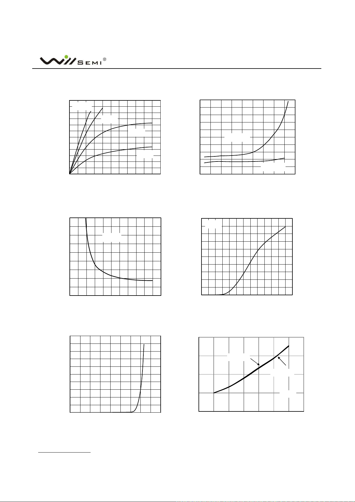
Typical Performance Characteristis
24
VGS=10V
20
16
12
8
,Drain Current(A)
D
I
4
0
012345
VDS,Drain-Source voltage(V)
VGS=6V
VGS=4V
VGS=3V
Drain Current VS Drain-Source voltage
0.11
0.09
0.07
0.05
ON Resistance(Ohm)
DS(ON)
0.03
R
0246810
VGS,Gate-Source Voltage(V)
ID=4.3A
120
100
80
VGS=4.5V
60
ON Resistance(mOhm)
40
DS(ON)
R
20
0 5 10 15 20
ID, Drain Current(A)
VGS=10V
Drain Current vs ON Resistance
25
VDS=2V
20
15
10
,Drain Current(A)
D
5
I
0
0123456
VGS,Gate-Source Voltage(V)
Gate-Source Voltage vs ON Resistance
1.5
1.2
0.9
0.6
0.3
IS, Source-Drain Current(A)
0.0
0.0 0.2 0.4 0.6 0.8
VDS,Drain-Source voltage(V)
Drain Current VS Source-Drain Current
http://www.willsemi.com Page 3
Drain Current VS Gate-Source Voltage
1.6
1.4
1.2
1
Normalized On-Resistance
0.8
0 25 50 75 100 125 150 175
VGS=-10V
VGS=-4.5V
Temperature (°C)
On-Resistance vs. Junction
Oct,
0 2012 Rev 2.
ID=-5A
2
 Loading...