

Willsemi WL2805N12, WL2805N13, WL2805N15, WL2805N18, WL2805N25 Schematic [ru]
...
WL2805N
Low power consumptionˈCMOS LDO
Descriptions
The WL2805N series are low dropout linear
regulators and optimized to provide a high
performance solution for battery power system to
deliver low quiescent current. The devices offer a new
level of cost effective performance in cellular phones,
laptop and notebook computers, and other portable
devices.
The WL2805N series are designed to make use of
low cost ceramic capacitors which ensure the stability
of the output current, and enhance the efficiency in
order to prolong the battery life of those portable
devices.
The WL2805N regulators are available in
SOT-23-3L packages. Standard products are Pb-free
and Halogen free products.
Features
z Quiescent current : 3A Typ.
z Input voltage : 2.2V ~ 5.5V
z Output voltage : 1.2V ~ 3.3V
z Output current : 250mA @ V
z Output current : 100mA @ V
z Dropout voltage : 100mV @ 100mA
z Recommend capacitor : 1uF
z Operating Temperature : -40 ~ +85 °C
z Output short protection
Applications
z MP3/MP4 Players
z Cell phones
z Bluetooth earphone
z Wireless mouse
z Others electronics devices
OUT
OUT
>2V
2V
WL2805N
Http://www.willsemi.com
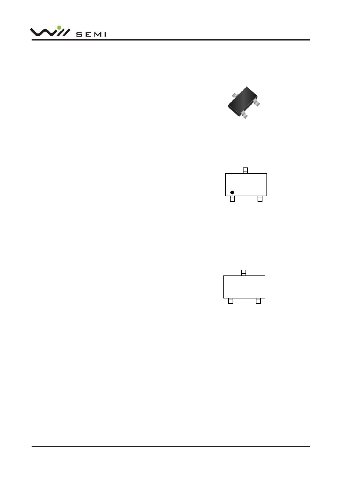
SOT-23-3L
VIN
3
1
2
GND VOUT
Pin Configuration (Top View)
For detail marking information please see page 8.
Order Information
For detail order information please see page 8.
****
Marking
Will Semiconductor Ltd. 1 Jun. 2011 – Rev1.4
WL2805N
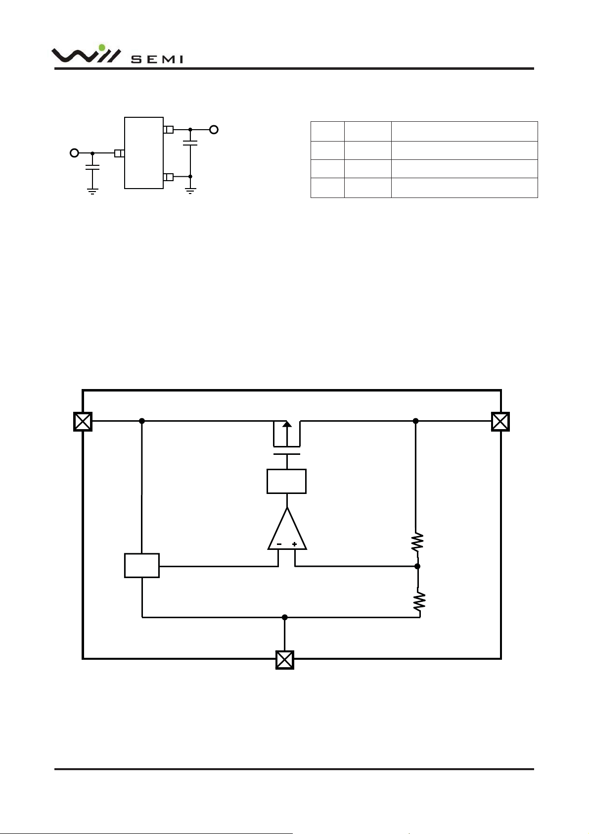
Typical Applications
VIN
1uF
3
Block Diagram
VIN
Vref
2
1
1uF
VOUT
OCP
GND
Pin Descriptions
PIN Symbol Description
1 GND Ground
2 VOUT Output
3 VIN Input
VOUT
Will Semiconductor Ltd. 2 Jun. 2011 – Rev1.4
WL2805N
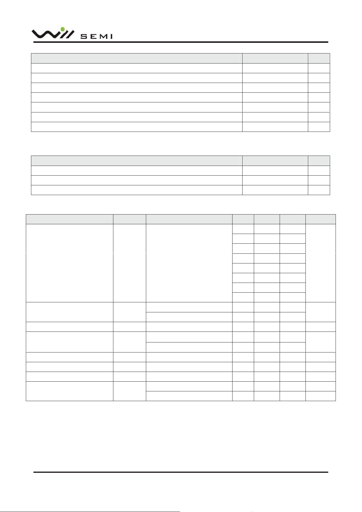
Absolute Maximum Ratings
Parameter Value Unit
Power Dissipation 300 mW
VIN Range
VEN Range
V
Range
OUT
Lead Temperature 260
Storage Temperature -65 ~ 150
Operating Junction Temperature 150
Operating Range
Parameter Value Unit
Thermal Resistance, R
417
JA
Input Voltage 2.2 ~ 5.5 V
Operating Temperature Range
Electronics Characteristics
Parameter Symbol Condition Min. Typ. Max. Unit
Output Voltage V
Output Current I
Output short current limiter I
Dropout Voltage V
Line Regulation
Load Regulation
Quiescent Current IQ V
Power Supply Ripple Rejection PSRR
(VIN = V
OUT
OUT
V
LIM
DROP
ƸV
LINE
ƸV
LOAD
OUT
V
= V
IN
V
OUT
V
OUT
OUT
I
OUT
I
OUT
V
IN=VOUT
I
OUT
= V
IN
Vp-p=1V, F=100Hz, I
Vp-p=1V, F=1KHz, I
+1V, CIN=C
=1uF, TA=25°C, unless otherwise noted)
OUT
1.170 1.200 1.230
1.270 1.300 1.330
1.470 1.500 1.530
1.764 1.800 1.836
OUT
+1V , I
OUT
=1mA
2.450 2.500 2.550
2.744 2.800 2.856
2.940 3.000 3.060
3.234 3.300 3.366
> 2V 250
2V
100
=GND 150 mA
=30mA, V
=100mA, V
+1V~6V, I
=3.0V 30 100
OUT
=3.0V 100 200
OUT
=40mA 0.1 %/V
OUT
= 1~ 100mA 25 mV
OUT
+1V, I
=0A 3 5
OUT
=10mA -50
OUT
=10mA -30
OUT
-0.36.0
-0.3V
-0.3V
IN
IN
-4085
V
V
V
o
C
o
C
o
C
o
C/W
o
C
V
mA
mV
uA
dB
dB
Will Semiconductor Ltd. 3 Jun. 2011 – Rev1.4
 Loading...