

Page 1

Page 2

This page intentionally left blank
Page 3

DIGITAL RADIO SYSTEM
DESIGN
Page 4

This page intentionally left blank
Page 5

DIGITAL RADIO
SYSTEM DESIGN
Grigorios Kalivas
University of Patras, Greece
A John Wiley and Sons, Ltd, Publication
Page 6

This edition first published 2009
© 2009 John Wiley & Sons Ltd.,
Registered office
John Wiley & Sons Ltd, The Atrium, Southern Gate, Chichester, West Sussex, PO19 8SQ, United Kingdom
For details of our global editorial offices, for customer services and for information about how to apply for
permission to reuse the copyright material in this book please see our website at www.wiley.com.
The right of the author to be identified as the author of this work has been asserted in accordance with the Copyright,
Designs and Patents Act 1988.
All rights reserved. No part of this publication may be reproduced, stored in a retrieval system, or transmitted, in any
form or by any means, electronic, mechanical, photocopying, recording or otherwise, except as permitted by the UK
Copyright, Designs and Patents Act 1988, without the prior permission of the publisher.
Wiley also publishes its books in a variety of electronic formats. Some content that appears in print may not be
available in electronic books.
Designations used by companies to distinguish their products are often claimed as trademarks. All brand names and
product names used in this book are trade names, service marks, trademarks or registered trademarks of their
respective owners. The publisher is not associated with any product or vendor mentioned in this book. This
publication is designed to provide accurate and authoritative information in regard to the subject matter covered. It is
sold on the understanding that the publisher is not engaged in rendering professional services. If professional advice
or other expert assistance is required, the services of a competent professional should be sought.
Library of Congress Cataloging-in-Publication Data
Kalivas, Grigorios.
Digital radio system design / Grigorios Kalivas.
p. cm.
Includes bibliographical references and index.
ISBN 978-0-470-84709-1 (cloth)
1. Radio—Transmitter-receivers—Design and construction. 2. Digital communications—Equipment and
supplies—Design and construction. 3. Radio circuits—Design and construction. 4. Signal processing—Digital
techniques. 5. Wireless communication systems—Equipment and supplies—Design and construction. I. Title.
TK6553.K262 2009
621.384
131—dc22 2009015936
A catalogue record for this book is available from the British Library.
ISBN 9780470847091 (H/B)
Set in 10/12 Times Roman by Macmillan Typesetting
Printed in Singapore by Markono
Page 7

To Stella, Maria and Dimitra and to the memory of my father
Page 8

This page intentionally left blank
Page 9

Contents
Preface xiii
1 Radio Communications: System Concepts, Propagation and Noise 1
1.1 Digital Radio Systems and Wireless Applications 2
1.1.1 Cellular Radio Systems 2
1.1.2 Short- and Medium-range Wireless Systems 3
1.1.3 Broadband Wireless Access 6
1.1.4 Satellite Communications 6
1.2 Physical Layer of Digital Radio Systems 7
1.2.1 Radio Platform 7
1.2.2 Baseband Platform 9
1.2.3 Implementation Challenges 10
1.3 Linear Systems and Random Processes 11
1.3.1 Linear Systems and Expansion of Signals in Orthogonal Basis Functions 11
1.3.2 Random Processes 12
1.3.3 White Gaussian Noise and Equivalent Noise Bandwidth 15
1.3.4 Deterministic and Random Signals of Bandpass Nature 16
1.4 Radio Channel Characterization 19
1.4.1 Large-scale Path Loss 19
1.4.2 Shadow Fading 22
1.4.3 Multipath Fading in Wideband Radio Channels 22
1.5 Nonlinearity and Noise in Radio Frequency Circuits and Systems 32
1.5.1 Nonlinearity 32
1.5.2 Noise 38
1.6 Sensitivity and Dynamic Range in Radio Receivers 44
1.6.1 Sensitivity and Dynamic Range 44
1.6.2 Link Budget and its Effect on the Receiver Design 44
1.7 Phase-locked Loops 46
1.7.1 Introduction 46
1.7.2 Basic Operation of Linear Phase-locked Loops 46
1.7.3 The Loop Filter 48
1.7.4 Equations and Dynamic Behaviour of the Linearized PLL 50
1.7.5 Stability of Phase-locked Loops 53
1.7.6 Phase Detectors 55
1.7.7 PLL Performance in the Presence of Noise 59
1.7.8 Applications of Phase-locked Loops 60
References 62
Page 10

viii Contents
2 Digital Communication Principles 65
2.1 Digital Transmission in AWGN Channels 65
2.1.1 Demodulation by Correlation 65
2.1.2 Demodulation by Matched Filtering 67
2.1.3 The Optimum Detector in the Maximum Likelihood Sense 69
2.1.4 Techniques for Calculation of Average Probabilities of Error 72
2.1.5 M -ary Pulse Amplitude Modulation (PAM) 73
2.1.6 Bandpass Signalling 75
2.1.7 M -ary Phase Modulation 82
2.1.8 Offset QPSK 89
2.1.9 Quadrature Amplitude Modulation 90
2.1.10 Coherent Detection for Nonideal Carrier Synchronization 93
2.1.11 M -ary Frequency Shift Keying 96
2.1.12 Continuous Phase FSK 98
2.1.13 Minimum Shift Keying 103
2.1.14 Noncoherent Detection 106
2.1.15 Differentially Coherent Detection (M -DPSK) 107
2.2 Digital Transmission in Fading Channels 112
2.2.1 Quadrature Amplitude Modulation 112
2.2.2 M -PSK Modulation 113
2.2.3 M -FSK Modulation 113
2.2.4 Coherent Reception with Nonideal Carrier Synchronization 114
2.2.5 Noncoherent M -FSK Detection 116
2.3 Transmission Through Band-limited Channels 117
2.3.1 Introduction 117
2.3.2 Baseband Transmission Through Bandlimited Channels 120
2.3.3 Bandlimited Signals for Zero ISI 122
2.3.4 System Design in Band-limited Channels of Predetermined Frequency Response 125
2.4 Equalization 128
2.4.1 Introduction 128
2.4.2 Sampled-time Channel Model with ISI and Whitening Filter 131
2.4.3 Linear Equalizers 134
2.4.4 Minimum Mean Square Error Equalizer 136
2.4.5 Detection by Maximum Likelihood Sequence Estimation 137
2.4.6 Decision Feedback Equalizer 138
2.4.7 Practical Considerations 139
2.4.8 Adaptive Equalization 140
2.5 Coding Techniques for Reliable Communication 141
2.5.1 Introduction 141
2.5.2 Benefits of Coded Systems 143
2.5.3 Linear Block Codes 143
2.5.4 Cyclic Codes 145
2.6 Decoding and Probability of Error 147
2.6.1 Introduction 147
2.6.2 Convolutional Codes 151
2.6.3 Maximum Likelihood Decoding 154
2.6.4 The Viterbi Algorithm for Decoding 156
2.6.5 Transfer Function for Convolutional Codes 157
2.6.6 Error Performance in Convolutional Codes 158
Page 11

Contents ix
2.6.7 Turbo Codes 159
2.6.8 Coded Modulation 162
2.6.9 Coding and Error Correction in Fading Channels 164
References 168
3 RF Transceiver Design 173
3.1 Useful and Harmful Signals at the Receiver Front-End 173
3.2 Frequency Downconversion and Image Reject Subsystems 175
3.2.1 Hartley Image Reject Receiver 177
3.2.2 Weaver Image Reject Receiver 180
3.3 The Heterodyne Receiver 183
3.4 The Direct Conversion Receiver 185
3.4.1 DC Offset 186
3.4.2 I–Q Mismatch 188
3.4.3 Even-Order Distortion 189
3.4.4 1/f Noise 189
3.5 Current Receiver Technology 190
3.5.1 Image Reject Architectures 190
3.5.2 The Direct Conversion Architecture 206
3.6 Transmitter Architectures 208
3.6.1 Information Modulation and Baseband Signal Conditioning 209
3.6.2 Two-stage Up-conversion Transmitters 210
3.6.3 Direct Upconversion Transmitters 211
References 211
4 Radio Frequency Circuits and Subsystems 215
4.1 Role of RF Circuits 216
4.2 Low-noise Amplifiers 219
4.2.1 Main Design Parameters of Low-noise Amplifiers 219
4.2.2 LNA Configurations and Design Trade-offs 222
4.3 RF Receiver Mixers 227
4.3.1 Design Considerations for RF Receiver Mixers 227
4.3.2 Types of Mixers 228
4.3.3 Noise Figure 232
4.3.4 Linearity and Isolation 235
4.4 Oscillators 235
4.4.1 Basic Theory 235
4.4.2 High-frequency Oscillators 239
4.4.3 Signal Quality in Oscillators 241
4.5 Frequency Synthesizers 243
4.5.1 Introduction 243
4.5.2 Main Design Aspects of Frequency Synthesizers 244
4.5.3 Synthesizer Architectures 247
4.5.4 Critical Synthesizer Components and their Impact on the System Performance 253
4.5.5 Phase Noise 256
4.6 Downconverter Design in Radio Receivers 258
4.6.1 Interfaces of the LNA and the Mixer 258
4.6.2 Local Oscillator Frequency Band and Impact of Spurious Frequencies 261
Page 12

x Contents
4.6.3 Matching at the Receiver Front-end 261
4.7 RF Power Amplifiers 263
4.7.1 General Concepts and System Aspects 263
4.7.2 Power Amplifier Configurations 264
4.7.3 Impedance Matching Techniques for Power Amplifiers 271
4.7.4 Power Amplifier Subsystems for Linearization 273
References 273
5 Synchronization, Diversity and Advanced Transmission Techniques 277
5.1 TFR Timing and Frequency Synchronization in Digital Receivers 277
5.1.1 Introduction 277
5.1.2 ML Estimation (for Feedback and Feed-forward) Synchronizers 280
5.1.3 Feedback Frequency/Phase Estimation Algorithms 282
5.1.4 Feed-forward Frequency/Phase Estimation Algorithms 286
5.1.5 Feedback Timing Estimation Algorithms 291
5.1.6 Feed-forward Timing Estimation Algorithms 293
5.2 Diversity 295
5.2.1 Diversity Techniques 295
5.2.2 System Model 296
5.2.3 Diversity in the Receiver 297
5.2.4 Implementation Issues 302
5.2.5 Transmitter Diversity 304
5.3 OFDM Transmission 306
5.3.1 Introduction 306
5.3.2 Transceiver Model 309
5.3.3 OFDM Distinct Characteristics 312
5.3.4 OFDM Demodulation 313
5.3.5 Windowing and Transmitted Signal 314
5.3.6 Sensitivities and Shortcomings of OFDM 315
5.3.7 Channel Estimation in OFDM Systems 339
5.4 Spread Spectrum Systems 342
5.4.1 Introduction and Basic Properties 342
5.4.2 Direct Sequence Spread Spectrum Transmission and Reception 348
5.4.3 Frequency Hopping SS Transmission and Reception 350
5.4.4 Spread Spectrum for Multiple Access Applications 352
5.4.5 Spreading Sequences for Single-user and Multiple Access DSSS 358
5.4.6 Code Synchronization for Spread Spectrum Systems 363
5.4.7 The RAKE Receiver 365
References 368
6 System Design Examples 371
6.1 The DECT Receiver 371
6.1.1 The DECT Standard and Technology 371
6.1.2 Modulation and Detection Techniques for DECT 372
6.1.3 A DECT Modem for a Direct Conversion Receiver Architecture 375
6.2 QAM Receiver for 61 Mb/s Digital Microwave Radio Link 394
6.2.1 System Description 394
6.2.2 Transmitter Design 396
Page 13

Contents xi
6.2.3 Receiver Design 397
6.2.4 Simulation Results 403
6.2.5 Digital Modem Implementation 406
6.3 OFDM Transceiver System Design 416
6.3.1 Introduction 416
6.3.2 Channel Estimation in Hiperlan/2 418
6.3.3 Timing Recovery 423
6.3.4 Frequency Offset Correction 424
6.3.5 Implementation and Simulation 435
References 438
Index 441
Page 14

This page intentionally left blank
Page 15

Preface
Radio communications is a field touching upon various scientific and engineering disciplines. From cellular radio, wireless networking and broadband indoor and outdoor radio to electronic surveillance, deep
space communications and electronic warfare. All these applications are based on radio electronic systems designed to meet a variety of requirements concerning reliable communication of information such
as voice, data and multimedia. Furthermore, the continuous demand for quality of communication and
increased efficiency imposes the use of digital modulation techniques in radio transmission systems
and has made it the dominant approach in system design. Consequently, the complete system consists of
a radio transmitter and receiver (front-end) and a digital modulator and demodulator (modem).
This book aims to introduce the reader to the basic principles of radio systems by elaborating on the
design of front-end subsystems and circuits as well as digital transmitter and receiver sections.
To be able to handle the complete transceiver, the electronics engineer must be familiar with diverse
electrical engineering fields like digital communications and RF electronics. The main feature of this
book is that it tries to accomplish such a demanding task by introducing the reader to both digital modem
principles and RF front-end subsystem and circuit design. Furthermore, for effective system design it is
necessary to understand concepts and factors that mainly characterize and impact radio transmission and
reception such as the radio channel, noise and distortion. Although the book tackles such diverse fields,
it treats them in sufficient depth to allow the designer to have a solid understanding and make use of
related issues for design purposes.
Recent advancements in digital processing technology made the application of advanced schemes (like
turbo coding) and transmission techniques like diversity, orthogonal frequency division multiplexing and
spread spectrum very attractive to apply in modern receiver systems.
Apart from understanding the areas of digital communications and radio electronics, the designer must
also be able to evaluate the impact of the characteristics and limitations of the specific radio circuits and
subsystems on the overall RF front-end system performance. In addition, the designer must match a link
budget analysis to specific digital modulation/transmission techniques and RF front-end performance
while at the same time taking into account aspects that interrelate the performance of the digital modem
with the characteristics of the RF front-end. Such aspects include implementation losses imposed by
transmitter–receiver nonidealities (like phase noise, power amplifier nonlinearities, quadrature mixer
imbalances) and the requirements and restrictions on receiver synchronization subsystems.
This book is intended for engineers working on radio system design who must account for every factor
in system and circuit design to producea detailed high-level design of the requiredsystem. Forthis reason,
the designer must have an overall and in-depth understanding of a variety of concepts from radio channel
characteristics and digital modem principles to silicon technology and RF circuit configuration for low
noise and low distortion design. In addition, the book is well suited for graduate students who study
transmitter/receiver system design as it presents much information involving the complete transceiver
chain in adequate depth that can be very useful to connect the diverse fields of digital communications
and RF electronics in a unified system concept.
To complete this book several people have helped in various ways. First of all I am indebted to
my colleagues Dimitrios Toumpakaris and Konstantinos Efstathiou for reading in detail parts of the
manuscript and providing me with valuable suggestions which helped me improve it on various levels.
Page 16

xiv Preface
Further valuable help came from my graduate and ex-graduate students Athanasios Doukas, Christos
Thomos and Dr Fotis Plessas, who helped me greatly with the figures. Special thanks belong to Christos
Thomos, who has helped me substantially during the last crucial months on many levels (proof-reading,
figure corrections, table of contents, index preparation etc.).
Page 17

1
Radio Communications: System Concepts, Propagation and Noise
A critical point for the development of radio communications and related applications was
the invention of the ‘super-heterodyne’ receiver by Armstrong in 1917. This system was used
to receive and demodulate radio signals by down-converting them in a lower intermediate
frequency (IF). The demodulator followed the IF amplification and filtering stages and was
used to extract the transmitted voice signal from a weak signal impaired by additive noise.
The super-heterodyne receiver was quickly improved to demodulate satisfactorily very weak
signals buried in noise (high sensitivity) and, at the same time, to be able to distinguish the
useful signals from others residing in neighbouring frequencies (good selectivity). These two
properties made possible the development of low-cost radio transceivers for a variety of applications. AM and FM radio were among the first popular applications of radio communications.
In a few decades packet radios and networks targeting militarycommunications gained increasing interest. Satellite and deep-space communications gave the opportunity to develop very
sophisticated radio equipment during the 1960s and 1970s. In the early 1990s, cellular communications and wireless networking motivated a very rapid development of low-cost, low-power
radios which initiated the enormous growth of wireless communications.
The biggest development effort was the cellular telephone network. Since the early 1960s
there had been a considerable research effort by the AT&T Bell Laboratories to develop a
cellular communication system. By the end of the 1970s the system had been tested in the field
and at the beginning ofthe 1980s the first commercial cellular systems appeared. Theincreasing
demand for higher capacity, low cost, performance and efficiency led to the second generation
of cellular communication systems in the 1990s. To fulfill the need for high-quality bandwidthdemanding applications like data transmission, Internet, web browsing and video transmission,
2.5G and 3G systems appeared 10 years later.
Along with digital cellular systems, wireless networking and wireless local area networks
(WLAN) technology emerged. The need to achieve improved performance in a harsh propagation environment like the radio channel led to improved transmission technologies like spread
spectrum and orthogonal frequency division multiplexing (OFDM). These technologies were
Digital Radio System Design Grigorios Kalivas
© 2009 John Wiley & Sons, Ltd
Page 18

2 Digital Radio System Design
put to practice in 3G systems like wideband code-division multiple access (WCDMA) as well
as in high-speed WLAN like IEEE 802.11a/b/g.
Different types of digital radio system have been developed during the last decade that are
finding application in wireless personal area networks (WPANs). These are Bluetooth and
Zigbee, which are usedto realize wireless connectivity of personal devicesand home appliances
like cellular devices and PCs. Additionally, they are also suitable for implementing wireless
sensor networks (WSNs) that organize in an ad-hoc fashion. In all these, the emphasis is mainly
on short ranges, low transmission rates and low power consumption.
Finally, satellite systems are being constantly developed to deliver high-quality digital video
and audio to subscribers all over the world.
The aims of this chapter are twofold. The first is to introduce the variety of digital radio
systems and their applications along with fundamental concepts and challenges of the basic
radio transceiver blocks (the radio frequency, RF, front-end and baseband parts). The second is
to introduce the reader to the technical background necessary to address the main objective of
the book, which is the design of RF and baseband transmitters and receivers. For this purpose
we present the basic concepts of linear systems, stochastic processes, radio propagation and
channel models. Along with these we present in some detail the basic limitations of radio
electronic systems and circuits, noise and nonlinearities. Finally, we introduce one of the most
frequently used blocks of radio systems, the phase-locked loop (PLL), which finds applications
in a variety of subsystems in a transmitter/receiver chain, such as the local oscillator, the carrier
recovery and synchronization, and coherent detection.
1.1 Digital Radio Systems and Wireless Applications
The existence of a large number of wireless systems for multiple applications considerably
complicates the allocation of frequency bands to specific standards and applications across
the electromagnetic spectrum. In addition, a number of radio systems (WLAN, WPAN, etc.)
operating in unlicensed portions of the spectrum demand careful assignment of frequency
bands and permitted levels of transmitted power in order to minimize interference and permit
the coexistence of more than one radio system in overlapping or neighbouring frequency bands
in the same geographical area.
Below we present briefly most of the existing radio communication systems, giving some
information on the architectures, frequency bands, main characteristics and applications of
each one of them.
1.1.1 Cellular Radio Systems
A cellular system is organized in hexagonal cells in order to provide sufficient radio coverage
to mobile users moving across the cell. A base station (BS) is usually placed at the centre of the
cell for that purpose. Depending on theenvironment (rural or urban), the areas of thecells differ.
Base stations are interconnected through a high-speed wired communications infrastructure.
Mobile users can have an uninterrupted session while moving through different cells. This is
achieved by the MTSOs acting as network controllers of allocated radio resources (physical
channels and bandwidth) to mobile users through the BS. In addition, MTSOs are responsible
for routing all calls associated with mobile users in their area.
Second-generation (2G) mobile communications employed digital technology to reduce
cost and increase performance. Global system for mobile communications (GSM) is a very
Page 19

Radio Communications: System Concepts, Propagation and Noise 3
successful 2G system that was developed and deployed in Europe. It employs Gaussian minimum shift keying (MSK) modulation, which is a form of continuous-phase phase shift keying
(PSK). The access technique is based on time-division multiple access (TDMA) combined
with slow frequency hopping (FH). The channel bandwidth is 200 kHz to allow for voice and
data transmission.
IS-95 (Interim standard-95) is a popular digital cellular standard deployed in the USA using
CDMA access technology and binary phase-shift keying (BPSK) modulation with 1.25 MHz
channel bandwidth. In addition, IS-136 (North American Digital Cellular, NADC) is another
standard deployed in North America. It utilizes 30 kHz channels and TDMAaccess technology.
2.5G cellular communication emerged from 2G because of the need for higher transmission
rates to support Internet applications, e-mail and web browsing. General Packet Radio Service
(GPRS) and Enhanced Data Rates for GSM Evolution (EGDE) are the two standards designed
as upgrades to 2G GSM. GPRS is designed to implement packet-oriented communication
and can perform network sharing for multiple users, assigning time slots and radio channels
[Rappaport02]. In doing so, GPRS can support data transmission of 21.4 kb/s for each of the
eight GSM time slots. One user can use all of the time slots to achieve a gross bit rate of
21.4 ×8 =171.2 kb/s.
EDGE is another upgrade of the GSM standard. It is superior to GPRS in that it can operate
using nine different formats in air interface [Rappaport02]. This allows the system to choose
the type and quality of error control. EDGE uses 8-PSK modulation and can achieve a maximum throughput of 547.2 kb/s when all eight time slots are assigned to a single user and no
redundancy is reserved for error protection. 3G cellular systems are envisaged to offer highspeed wireless connectivity to implement fast Internet access, Voice-over-Internet Protocol,
interactive web connections and high-quality, real-time data transfer (for example music).
UMTS (Universal Mobile Telecommunications System) is an air interface specified in
the late 1990s by ETSI (European Telecommunications Standards Institute) and employs
WCDMA, considered one of the more advanced radio access technologies. Because of the
nature of CDMA, the radio channel resources are not divided, but they are shared by all users.
For that reason, CDMA is superior to TDMA in terms of capacity. Furthermore, each user
employs a unique spreading code which is multiplied by the useful signal in order to distinguish
the users and prevent interference among them. WCDMA has 5 MHz radio channels carrying
data rates up to 2 Mb/s. Each 5 MHz channel can offer up to 350 voice channels [Rappaport02].
1.1.2 Short- and Medium-range Wireless Systems
The common characteristic of these systems is the range of operation, which is on the order
of 100 m for indoor coverage and 150–250 m for outdoor communications. These systems are
mostly consumer products and therefore the main objectives are low prices and low energy
consumption.
1.1.2.1 Wireless Local Area Networks
Wireless LANs were designed toprovide high-data-rate, high-performance wireless connectivity within a short range in theform of a network controlled by a number of central points (called
access points or base stations). Access points are used to implement communication between
two users by serving as up-link receivers and down-link transmitters. The geographical area
Page 20

4 Digital Radio System Design
of operation is usually confined to a few square kilometres. For example, a WLAN can be
deployed in a university campus, a hospital or an airport.
The second and third generation WLANs proved to be the most successful technologies.
IEEE 802.11b (second generation) operates in the 2.4 GHz ISM (Industral, Scientific and
Medical) band within a spectrum of 80MHz. It uses direct sequence spread spectrum (DSSS)
transmission technology with gross bit rates of 1, 2, 5 and 11 Mb/s. The 11 Mb/s data rate
was adopted in late 1998 and modulates data by using complementary code keying (CCK)
to increase the previous transmission rates. The network can be formulated as a centralized
network using a number of access points. However, it can also accommodate peer-to-peer
connections.
The IEEE 802.11a standard was developed as the third-generation WLAN and was designed
to provide even higher bit rates (up to 54 Mb/s). It uses OFDM transmission technology and
operates in the 5 GHz ISM band. In the USA, the Federal Communications Commission (FCC)
allocated two bands each 100 MHz wide (5.15–5.25 and 5.25–5.35 GHz), and a third one at
5.725–5.825 GHz for operation of 802.11a. In Europe, HIPERLAN 2 was specified as the
standard for 2G WLAN. Its physical layer is very similar to that of IEEE 802.11a. However,
it uses TDMA for radio access instead of the CSMA/CA used in 802.11a.
The next step was to introduce the 802.11g, which mostly consisted of a physical layer specification at 2.4 GHz with data rates matching those of 802.11a (up to 54 Mb/s). To achieve that,
OFDM transmission was set as a compulsory requirement. 802.11g is backward-compatible
to 802.11b and has an extended coverage range compared with 802.11a. To cope with issues
of quality of service, 802.11e was introduced, which specifies advanced MAC techniques to
achieve this.
1.1.2.2 WPANs and WSNs
In contrast to wireless LANs, WPAN standardization efforts focused primarily on lower transmission rates with shorter coverage and emphasis on low power consumption. Bluetooth (IEEE
802.15.1), ZigBee (IEEE 802.15.4)and UWB (IEEE802.15.3) represent standardsdesigned for
personal area networking. Bluetooth is an open standard designed for wireless data transfer
for devices located a few metres apart. Consequently, the dominant application is the wireless
interconnection of personal devices like cellular phones, PCs and their peripherals. Bluetooth
operates in the 2.4 GHz ISM band andsupports data and voice traffic withdata rates of 780 kb/s.
It uses FH as an access technique. It hops in a pseudorandom fashion, changing frequency carrier 1600 times per second (1600 hops/s). It can hop to 80 different frequency carriers located
1 MHz apart. Bluetooth devices are organized in groups of two to eight devices (one of which is
a master) constituting a piconet. Each device of a piconet has an identity (device address) that
must be known to all members of the piconet. The standard specifies two modes of operation:
asynchronous connectionless (ACL) in one channel (used for data transfer at 723 kb/s) and
synchronous connection-oriented (SCO) for voice communication (employing three channels
at 64 kb/s each).
A scaled-down version of Bluetooth is ZigBee, operating on the same ISM band. Moreover, the 868/900 MHz band is used for ZigBee in Europe and North America. It supports
transmission rates of up to 250 kb/s covering a range of 30 m.
During the last decade, WSNs have emerged as a new field for applications of low-power
radio technology. In WSN, radio modules are interconnected, formulating ad-hoc networks.
Page 21

Radio Communications: System Concepts, Propagation and Noise 5
WSN find many applications in the commercial, military and security sectors. Such applications concern home and factory automation, monitoring, surveillance, etc. In this case,
emphasis is given to implementing a complete stack for ad hoc networking. An important
feature in such networks is multihop routing, according to which information travels through
the network by using intermediate nodes between the transmitter and the receiver to facilitate reliable communication. Both Bluetooth and ZigBee platforms are suitable for WSN
implementation [Zhang05], [Wheeler07] as they combine low-power operation with network
formation capability.
1.1.2.3 Cordless Telephony
Cordless telephony was developed to satisfy the needs for wireless connectivity to the public
telephone network (PTN). It consists of one or more base stations communicating with one or
more wireless handsets. The base stations are connected to the PTN through wireline and are
able to provide coverage of approximately 100 m in their communication with the handsets.
CT-2 isa second-generationcordless phone system developed in the 1990s with extended range
of operation beyond the home or office premises.
On the other hand, DECT (Digital European Cordless Telecommunications) was developed
such that it can support local mobility in an office building through a private branch exchange
(PBX) system. In this way, hand-off is supported between the different areas covered by the
base stations. The DECT standard operates in the 1900 MHz frequency band. Personal handyphone system (PHS) is a more advanced cordless phone system developed in Japan which can
support both voice and data transmission.
1.1.2.4 Ultra-wideband Communications
A few years ago, a spectrum of 7.5 GHz (3.1–10.6 GHz) was given for operation of ultrawideband (UWB) radio systems. The FCC permitted very low transmitted power, because
the wide area of operation of UWB would produce interference to most commercial and even
military wireless systems. There are two technology directions for UWB development. Pulsed
ultra-wideband systems (P-UWB) convey information by transmitting very short pulses (of
duration in the order of 1 ns). On the other hand, multiband-OFDM UWB (MB-OFDM)
transmits information using the OFDM transmission technique.
P-UWB uses BPSK, pulse position modulation (PPM) and amplitude-shift keying (ASK)
modulation and it needs a RAKE receiver (a special type of receiver used in Spread Spectrum
systems) to combine energy from multipath in order to achieve satisfactory performance. For
very high bit rates (on the order of 500Mb/s) sophisticated RAKE receivers must be employed,
increasing the complexity of the system. On the other hand, MB-UWB uses OFDM technology
to eliminate intersymbol interference (ISI) created by high transmission rates and the frequency
selectivity of the radio channel.
Ultra-wideband technology can cover a variety of applications ranging from low-bit-rate,
low-power sensor networks to very high transmission rate (over 100 Mb/s) systems designed
to wirelessly interconnect home appliances (TV, PCs and consumer electronic appliances). The
low bit rate systems are suitable for WSN applications.
P-UWB is supported by the UWB Forum, which has more than 200 members and focuses
on applications related to wireless video transfer within the home (multimedia, set-top boxes,
Page 22

6 Digital Radio System Design
DVD players). MB-UWB is supported by WiMediaAlliance, alsowith more than 200 members.
WiMedia targets applications related to consumer electronics networking (PCs TV, cellular
phones). UWB Forum will offer operation at maximum data rates of 1.35 Gb/s covering distances of 3 m [Geer06]. On the otherhand, WiMediaAlliance willprovide 480 Mb/s at distances
of 10 m.
1.1.3 Broadband Wireless Access
Broadband wireless can deliver high-data-rate wireless access (on the order of hundreds of
Mb/s) to fixed access points which in turn distribute it in a local premises. Business and residential premises are served by a backbone switch connected at the fixed access point and
receive broadband services in the form of local area networking and video broadcasting.
LMDS (local multipoint distribution system) and MMDS (multichannel multipoint distribution services) are two systems deployed in the USA operating in the 28 and 2.65 GHz bands.
LMDS occupies 1300 MHz bandwidth in three different bands around 28, 29 and 321 GHz and
aims to provide high-speed data services, whereas MMDS mostly provides telecommunications services [Goldsmith05] (hundreds of digital television channels and digital telephony).
HIPERACCESS is the European standard corresponding to MMDS.
On the other hand, 802.16 standard is being developedto specify fixed and mobile broadband
wireless access with high data rates and range of a few kilometres. It is specified to offer
40 Mb/s for fixed and 15 Mb/s for mobile users. Known as WiMAX, it aims to deliver multiple
services in long ranges by providing communication robustness, quality of service (QoS) and
high capacity, serving as the ‘last mile’ wireless communications. In that capacity, it can
complement WLAN and cellular access. In the physical layer it is specified to operate in bands
within the 2–11 GHz frequency range and uses OFDM transmission technology combined
with adaptive modulation. In addition, it can integrate multiple antenna and smart antenna
techniques.
1.1.4 Satellite Communications
Satellite systems are mostly used to implement broadcasting services with emphasis on highquality digital video and audio applications (DVB, DAB). The Digital Video Broadcasting
(DVB) project specified the first DVB-satellite standard (DVB-S) in 1994 and developed the
second-generation standard (DVB-S2) for broadband services in 2003. DVB-S3 is specified to
deliver high-quality video operating in the 10.7–12.75 GHz band. The high data rates specified
by the standard can accommodate up to eight standard TV channels per transponder. In addition
to standard TV, DVB-S provides HDTV services and is specified for high-speed Internet
services over satellite.
In addition to DVB, new-generation broadband satellite communications have been
developed to support high-data-rate applications and multimedia in the framework of
fourth-generation mobile communication systems [Ibnkahla04].
Direct-to-Home (DTH) satellite systems are used in North America and constitute two
branches: the Broadcasting Satellite Service (BSS) and the Fixed Satellite Service (FSS). BSS
operates at 17.3–17.8 GHz (uplink) and 12.2–12.7 GHz (downlink), whereas the bands for FSS
are 14–14.5 and 10.7–11.2 GHz, respectively.
Page 23

Radio Communications: System Concepts, Propagation and Noise 7
Finally, GPS (global positioning satellite) is an ever increasing market for providing localization services (location finding, navigation) and operates using DSSS in the
1500 MHz band.
1.2 Physical Layer of Digital Radio Systems
Radio receivers consist of an RF front-end, a possible IF stage and the baseband platform
which is responsible for the detection of the received signal after its conversion from analogue
to digital through an A/D converter. Similarly, on the transmitter side, the information signal is
digitally modulated and up-converted to a radio frequency band for subsequent transmission.
In the next section we use the term ‘radio platform’to loosely identify allthe RF and analogue
sections of the transmitter and the receiver.
1.2.1 Radio Platform
Considering the radio receiver, the main architectures are the super-heterodyne (SHR) and the
direct conversion receiver (DCR). These architectures are examined in detail in Chapter 3, but
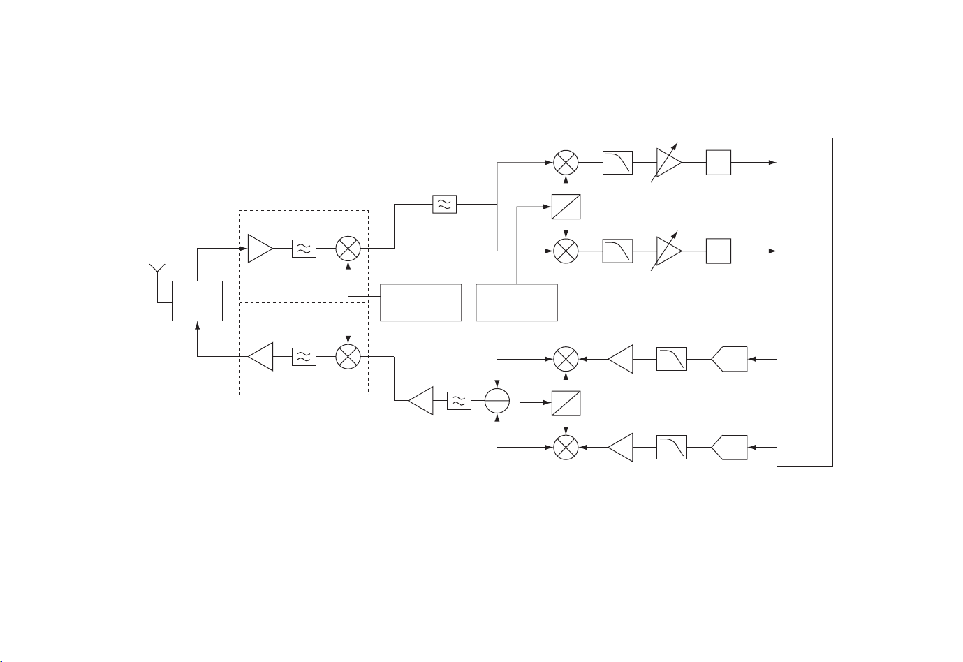
here we give some distinguishing characteristics as well as theirmain advantages and disadvantages in the context of some popular applications of radio system design. Figure 1.1 illustrates
the general structure of a radio transceiver. The SHR architecture involves a mixing stage just
after the low-noise amplifier (LNA) at the receiver or prior to the transmitting medium-power
and high-power amplifiers (HPA). Following this stage, there is quadrature mixing bringing the
received signal down to the baseband. Following mixers, there is variable gain amplification
and filtering to increase the dynamic range (DR) and at the same time improve selectivity.
When the local oscillator (LO) frequency is set equal to the RF input frequency, the received
signal is translated directly down to the baseband. The receiver designed following this
approach is called Direct conversion Receiver or zero-IF receiver. Such an architecture eliminates the IF and the corresponding IF stage at the receiver, resulting in less hardware but, as
we will see in Chapter 3, it introduces several shortcomings that can be eliminated with careful
design.
Comparing the two architectures, SHR is advantageous when a very high dynamic range
is required (as for example in GSM). In this case, by using more than one mixing stage,
amplifiers with variable gain are inserted between stages to increase DR. At the same time,
filtering inserted between two mixing stages becomes narrower, resulting in better selectivity
[Schreir02].
Furthermore, super-heterodyne can be advantageous compared with DCR when large
in-band blocking signals have to be eliminated. In DCR, direct conversion (DC) offset would
change between bursts, requiring its dynamic control [Tolson99].
Regarding amplitude and phase imbalances of the two branches, In-phase (I-phase) and
Q-phase considerably reduce the image rejection in SHR. In applications where there can be
no limit to the power of the neighbouring channels (like the ISM band), it is necessary to have
an image rejection (IR) on the order of 60 dB. SHR can cope with the problem by suitable
choice of IF frequencies [Copani05]. At the same time, more than one down-converting stage
relaxes the corresponding IR requirements. On the other hand, there is no image band in
DCR and hence no problem associated with it. However, in DCR, imbalances at the I–Q
Page 24
A/D
RF Down Converter
Transmit/
8
Receive
Switch
RF Up Converter
RF Synthesized
Local Oscillator
IF Synthesized
Local Oscillator
0
90
A/D
Digital
Baseband
Processor
D/A
0
90
D/A
Figure 1.1 General structure of a radio transmitter and receiver
Page 25

Radio Communications: System Concepts, Propagation and Noise 9
mixer create problems from the self-image and slightly deteriorate the receiver signal-to-noise
ratio (SNR) [Razavi97]. This becomes more profound in high-order modulation constellations
(64-QAM, 256-QAM, etc.)
On the other hand, DCR is preferred when implementation cost and high integration are
the most important factors. For example, 3G terminals and multimode transceivers frequently
employ the direct conversion architecture. DC offset and 1/f noise close to the carrier are
the most frequent deficiencies of homodyne receivers, as presented in detail in Chapter 3.
Furthermore, second-order nonlinearities can also create a problem at DC. However, digital
and analogue processing techniques can be used to eliminate these problems.
Considering all the above and from modern transceiver design experience, SHR is favoured
in GSM, satellite and millimetre wave receivers, etc. On the other hand, DCR is favoured in
3G terminals, Bluetooth and wideband systems like WCDMA, 802.11a/b/g, 802.16 and UWB.
1.2.2 Baseband Platform
The advent of digital signal processors (DSP) and field-programmable gate arrays (FPGAs),
dramatically facilitated the design and implementation of very sophisticated digital demodulators and detectors for narrowband and wideband wireless systems. 2G cellular radio
uses GMSK, a special form of continuous-phase frequency-shift keying (CPFSK). Gaussian
minimum-shift keying (GMSK)modem (modulator–demodulator) implementationcan be fully
digital and can be based on simple processing blocks like accumulators, correlators and lookup tables (LUTs) [Wu00], [Zervas01]. FIR (Finite Impulse Response) filters are always used
to implement various forms of matched filters. Coherent demodulation in modulations with
memory could use more complex sequential receivers implementing the Viterbi algorithm.
3G cellular radios and modern WLAN transceivers employ advanced transmission techniques using either spread spectrum or OFDM to increase performance. Spread spectrum
entails multiplication of the information sequence by a high-bit-rate pseudorandom noise (PN)
sequence operating at speeds which are multiples of the information rate. The multiple bandwidth of the PN sequence spreads information and narrowband interference to a band with
a width equal to that of the PN sequence. Suitable synchronization at the receiver restores
information at its original narrow bandwidth, but interference remains spread due to lack of
synchronization. Consequently, passing the received signal plus spread interference through a
narrow band filter corresponding to the information bandwidth reduces interference considerably. In a similar fashion, this technique provides multipath diversity at the receiver, permitting
the collection and subsequent constructive combining of the main and the reflected signal components arriving at the receiver. This corresponds to the RAKE receiver principle, resembling
a garden rake that is used to collect leaves. As an example, RAKE receivers were used to cope
with moderate delay spread and moderate bit rates (60 ns at the rate of 11 Mb/s [VanNee99].
To face large delay spreads at higher transmission rates, the RAKE receiver was combined
with equalization. On the other hand, OFDM divides the transmission bandwidth into many
subchannels, each one occupying a narrow bandwidth. In this way, owing to the increase in
symbol duration, the effect of dispersion in time of the reflected signal on the receiver is minimized. The effect of ISI is completely eliminated by inserting a guard band in the resulting
composite OFDM symbol. Fast Fourier transform (FFT) is an efficient way to produce
(in the digital domain) the required subcarriers over which the information will be embedded.
In practice, OFDM is used in third-generation WLANs, WiMAX and DVB to eliminate ISI.
Page 26

10 Digital Radio System Design
From the above discussion it is understood that, in modern 3G and WLAN radios, advanced
digital processing is required to implement the modem functions which incorporate transmission techniques like spread spectrum and OFDM. This can be performed using DSPs [Jo04],
FPGAs [Chugh05], application-specific integrated circuits (ASICs) or a combination of them
all [Jo04].
1.2.3 Implementation Challenges
Many challenges to the design and development of digital radio systems come from the necessity to utilize the latest process technologies (like deep submicron complementary metal-oxide
semiconductor, CMOS, processes) in order to save on chip area and power consumption.
Another equally important factor has to do with the necessity to develop multistandard and
multimode radios capable of implementing two or more standards (or more than one mode
of the same standard) in one system. For example, very frequently a single radio includes
GSM/GPRS and Bluetooth. In this case, the focus is on reconfigurable radio systems targeting
small, low-power-consumption solutions.
Regarding the radio front-end and related to the advances in process technology, some
technical challenges include:
•
reduction of the supply voltage while dynamic range is kept high [Muhammad05];
•
elimination of problems associated with integration-efficient architectures like the direct
conversion receiver; such problems include DC offset, 1/f noise and second order
nonlinearities;
•
low-phase-noise local oscillators to accommodate for broadband and multistandard system
applications;
•
wideband passive and active components (filters and low-noise amplifiers) just after the
antenna to accommodate for multistandard and multimode systems as well as for emerging
ultrawideband receivers;
For all the above RF front-end-related issues a common target is to minimize energy
dissipation.
Regarding the baseband section of the receiver, reconfigurability poses considerable challenges as it requires implementation of multiple computationally intensive functions (like FFT,
spreading, despreading and synchronization and decoding) in order to:
•
perform hardware/software partition that results in the best possible use of platform
resources;
•
define the architecture based on the nature of processing; for example, parallel and
computationally intensive processing vs algorithmic symbol-level processing [Hawwar06];
•
implement the multiple functionalities of the physical layer, which can include several
kinds of physical channels (like dedicated channels or synchronization channels), power
control and parameter monitoring by measurement (e.g. BER, SNR, signal-to-interference
ratio, SIR).
The common aspect of all the above baseband-related problems is to design the digital
platform such that partition of the functionalities in DSP, FPGAs and ASICs is implemented
in the most efficient way.
Page 27

Radio Communications: System Concepts, Propagation and Noise 11
1.3 Linear Systems and Random Processes
1.3.1 Linear Systems and Expansion of Signals in Orthogonal
Basis Functions
A periodic signal s(t) of bandwidth BScan be fully reproduced by N samples per period T,
spaced 1/(2B
of dimension N =2B
time waveforms like s(t). Hence, we can define the inner product of two signals s(t) and y(t)
in an interval [c
Using this, a group of signals ψ
) seconds apart (Nyquist’s theorem). Hence, s(t) can be represented by a vector
S
T. Consequently, most of the properties of vector spaces are true for
S
, c2] as:
1
c
s(t), y(t)=
(t) is defined as orthonormal basis if the following is satisfied:
n
ψ
(t), ψm(t)= δmn=
n
2
s(t)y∗(t)dt (1.1)
c
1
1, m = n
0, m = n
(1.2)
This is used to expand all signals {s
In this case, ψ
(t) is defined as a complete basis for {sm(t), m = 1, 2, ...M } and we have:
n
s
(t) =
m
(t), m = 1, 2, ...M } in terms of the functions ψn(t).
m
smkψk(t), smk=
k
T
sm(t)ψk(t)dt (1.3)
0
This kind of expansion is of great importance in digital communications because the group
{s
(t), m =1, 2,...M }represents allpossible transmitted waveforms in atransmission system.
m
Furthermore, if y
(t) is the output of a linear system with input sm(t) which performs
m
operation H[·], then we have:
y
(t) = H [sm(t)] =
m
smkH[ψk(t)] (1.4)
k
The above expression provides an easy way to find the response of a system by determining the
response of it, when the basis functions ψ
(t) are used as inputs.
n
In our case the system is the composite transmitter–receiver system with an overall impulse
response h(t) constituting, in most cases, the cascading three filters, the transmitter filter, the
channel response and the receiver filter. Hence the received signal will be expressed as
the following convolution:
(t) = sm(t) ∗ h(t) (1.5)
y
m
For example, as shown in Section 2.1, in an ideal system where the transmitted signal is only
corrupted by noise we have:
T
r(t) = s
(t) + n(t), rk=
m
r(t)ψk(t)dt = smk+ n
0
k
(1.6)
Based on the orthonormal expansion
s
(t) =
m
smkψk(t)
k
Page 28

12 Digital Radio System Design
of signal sm(t) as presented above, it can be shown [Proakis02] that the power content of a
periodic signal can be determined by the summation of the power of its constituent harmonics.
This is known as the Parseval relation and is mathematically expressed as follows:
tC+T
t
C
0
|sm(t)|2dt =
1
T
0
+∞
k=−∞
|smk|
2
(1.7)
1.3.2 Random Processes
Figure 1.2 shows an example for a random process X (t) consisting of sample functions xEi(t).
Since, as explained above, the random process at a specific time instant t
a random variable, the mean (or expectation function) and autocorrelation function can be
defined as follows:
∞
, t2) = E[X (t1)X (t2)] =
R
XX(t1
E{X (t
)}=mX(tC) =
C
−∞
+∞
+∞
−∞
−∞
xp
(x)dx (1.8)
X (tC)
x1x2p
X (t1)X (t2)
(x1, x2)dx1dx
Wide-sense stationary (WSS) is a process for which the mean is independent of t and its
autocorrelation is a function of the time difference t
and t2[RX(t1−t2) =RX(τ)].
t
1
=τ and not of the specific values of
1−t2
A random process is stationary if its statistical properties do not depend on time. Stationarity
is a stronger property compared with wide-sense stationarity.
Two important properties of the autocorrelation function of stationary processes are:
corresponds to
C
2
(1.9)
(−τ) =RX(τ), which means that it is an even function;
(1) R
X
(2) R
(τ) has a maximum absolute value at τ =0, i.e. |RX(τ)|≤RX(0).
X
Ergodicity is a very useful concept in random signal analysis. A stationary process is ergodic
if, for all outcomes E
and for all functions f (x), the statistical averages are equal to time
i
averages:
T/2
E{f [X (t)]}= lim
T→∞
1
T
f [xEi(t)]dt (1.10)
−T/2
1.3.2.1 Power Spectral Density of Random Processes
It is not possible to define a Fourier transform for random signals. Thus, the concept of power
spectral density (PSD) is introduced for random processes. To do that the following steps are
taken:
(1) Truncate the sample functions of a random process to be nonzero for t < T :
x
(t), 0 ≤ t ≤ T
x
Ei
(t; T) =
Ei
0, otherwise
(1.11)
Page 29
Radio Communications: System Concepts, Propagation and Noise 13
x
(t)
E
1
t1t
2
0
(t)
x
E
2
t
0
(t)
x
E
N
0
) X(t2)
X(t
1
t
t
Figure 1.2 Sample functions of random process X (t)
(2) Determine |XTi( f )|2from the Fourier transform XTi( f ) of the truncated random process
(t; T). The power spectral density S
x
Ei
( f ) for xEi(t; T) is calculated by averaging over a
x
Ei
large period of time T:
T
= lim
T→∞
2
(1.12)
(t; T) [Proakis02]:
Ei
|
X
E
2
|
( f )
Ti
T
(1.13)
(3) Calculate the average E|X
( f ) =
S
X
Ti
E
i
S
= lim
( f )|
xEi( f )
2
lim
T→∞
T→∞
over all sample functions x
|
2
|
X
( f )
Ti
T
|XTi( f )|
Page 30

14 Digital Radio System Design
The above procedure converts the power-type signals to energy-type signals by setting them
to zero for t > T . In this way, power spectral density for random processes defined as above
corresponds directly to that of deterministic signals [Proakis02].
In practical terms, S
( f ) represents the average power that would be measured at frequency
X
f in a bandwidth of 1 Hz.
Extending the definitions of energy and power of deterministic signals to random processes,
we have for each sample function x
=x
E
i
(t):
Ei
2
(t)dt, Pi= lim
Ei
T→∞
1
2
(t)dt (1.14)
x
Ei
T
Since these quantities are random variables the energy and power of the random process X(t)
corresponding to sample functions x
E
X
(t) are defined as:
Ei
= E
X2(t)dt=RX(t, t)dt (1.15)
= Elim
P
X
T→∞
T/2
1
T
X2(t)dt=
−T/2
T/2
1
T
RX(t, t)dt (1.16)
−T/2
For stationary processes, the energy and power are:
= RX(0)
P
X
+∞
E
=
X
RX(0)dt (1.17)
−∞
1.3.2.2 Random Processes Through Linear Systems
If Y (t) is the output of alinear system with input thestationary random process X (t) and impulse
response h(t), the following relations are true for the means and correlation (crosscorrelation
and autocorrelation) functions:
+∞
= m
m
Y
X
(τ) = RX(τ) ∗h(−τ) (1.19)
R
XY
R
(τ) = RX(τ) ∗h(τ) ∗ h(−τ) (1.20)
Y
h(t)dt (1.18)
−∞
Furthermore, translation of these expressions in the frequency domain [Equations (1.21)–
(1.23)] provides powerful tools to determine spectral densities along the receiver chain in the
presence of noise.
m
= mXH(0) (1.21)
Y
S
( f ) = SX|H( f )|
Y
S
( f ) = SX( f )H∗( f ) (1.23)
YX
2
(1.22)
Page 31

Radio Communications: System Concepts, Propagation and Noise 15
1.3.2.3 Wiener–Khinchin Theorem and Applications
The power spectraldensity of arandom process X(t) isgiven as thefollowing Fourier transform:
(1.24)
S
( f ) = Flim
X
T→∞
T/2
1
T
RX(t + τ, t)dt
−T/2
provided that the integral within the brackets takes finite values.
If X (t) is stationary then its PSD is the Fourier transform of the autocorrelation function:
S
( f ) = F [RX(τ)] (1.25)
X
An important consequence of theWiener–Khinchin is that the total powerof the random process
is equal to the integral of the power spectral density:
∞
SX( f )df (1.26)
−∞
P
= Elim
X
T→∞
T/2
1
T
X2(t)dt=
−T/2
Another useful outcome is that, when the random process is stationary and ergodic, its power
spectral density is equal to the PSD of each sample function of the process x
S
( f ) = S
X
( f ) (1.27)
x
Ei
(t):
Ei
1.3.3 White Gaussian Noise and Equivalent Noise Bandwidth
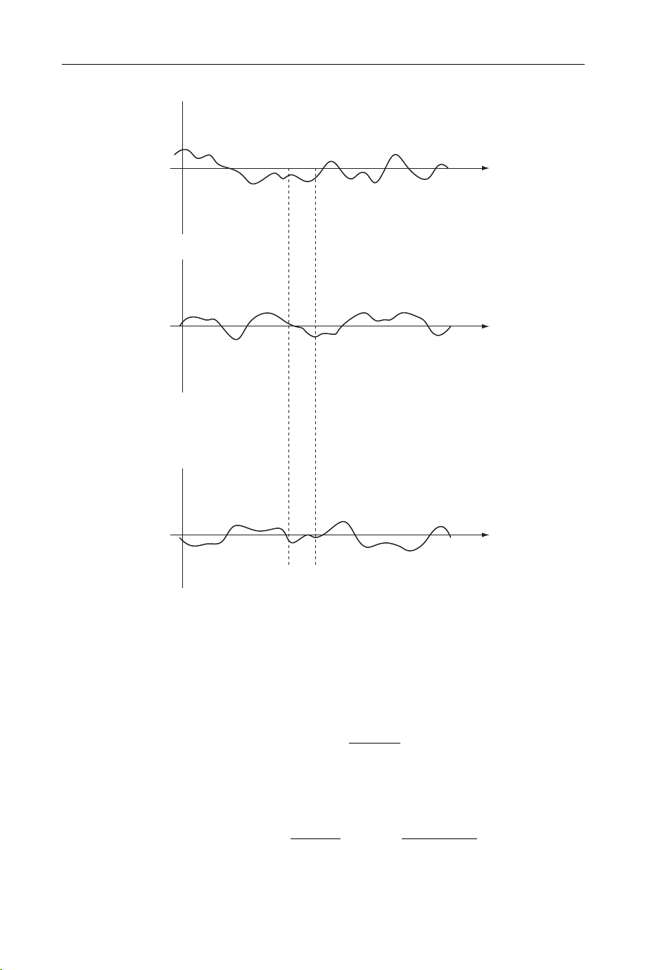
White noise is a random process N (t) having a constant power spectral density over all frequencies. Such a process does not exist but it was experimentally shown that thermal noise can
approximate N(t) well in reasonably wide bandwidth and has a PSD of value kT/2 [Proakis02].
Because the PSD of white noise has an infinite bandwidth, the autocorrelation function is a
delta function:
N
R
(τ) =
N
where N
=kT for white random process. The above formula shows that the random variables
0
associated with white noise are uncorrelated [because R
is also a Gaussian process, then the resulting random variables are independent. In practical
terms the noise used for the analysis of digital communications is considered white Gaussian,
stationary and ergodic process with zero mean. Usually, this noise is additive and is called
additive white Gaussian noise (AWGN).
If the above white noise passes through an ideal bandpass filter of bandwidth B, the resulting
random process is a bandpass white noise process. Its spectral density and autocorrelation
function are expressed as follows:
N
, |f |≤B/2
S
( f ) =
BN
0
0, |f |≥B/2
Noise equivalent bandwidth of a specific system refers to the bandwidth of an ideal reference
filter that will produce the same noise power at its output with the given system. More specifically, let the same white noise with PSD equal to N
frequency response |H
( f )| and a fictitious ideal (rectangular) filter, as shown in Figure 1.3.
F
We can define the constant magnitude of the ideal filter equal to the magnitude |H ( f )|
0
δ(τ) (1.28)
2
(τ) =0 for τ =0]. If white noise
N
, R
(τ) = N
BN
/2 pass through a filter Frwith a given
0
sin (πBτ)
0
πτ
(1.29)
of
ref
Page 32

16 Digital Radio System Design
f
2
HF( f )
2
H( f )
2
ref
B
neq
2
|
and ideal brick-wall filter with band-
H( f )
Figure 1.3 Equivalence between frequency response|HF(f )
width B
neq
Frat a reference frequency f
, which in most cases represents the frequency of maximum
ref
magnitude or the 3 dB frequency.
In this case, noise equivalent bandwidth is the bandwidth of the ideal brick-wall filter, which
will give the same noise power at its output as filter F
. The output noise power of the given
r
filter and the rectangular filter is:
To express B
∞
= N
P
N
we equate the two noise powers. Thus, we get:
neq
|H( f )|2df , PNr= N0|H( f )|
0
0
∞
|H( f )|2df
B
neq
0
=
|H( f )|
2
f
ref
2
B
neq
f
ref
(1.30)
(1.31)
1.3.4 Deterministic and Random Signals of Bandpass Nature
In communications, a high-frequency carrier is used to translate the information signal into
higher frequency suitable for transmission. For purposes of analysis and evaluation of the
performance of receivers, it is important to formulate such signals and investigate their
properties.
A bandpass signal is defined as one for which the frequency spectrum X( f ) is nonzero within
a bandwidth W around a high frequency carrier f
X ( f ) =
nonzero, |f − f
zero, |f − f
It is customary to express high frequency modulated signals as:
:
C
|≤W
C
|≥W
C
(1.32)
x(t) = A(t) cos [2πf
t + θ(t)] = Re[A(t) exp ( j2πfCt) exp ( jθ(t))] (1.33)
C
A(t) and θ(t) correspond to amplitude and phase which can contain information. Since the
carrier f
does not contain information, we seek expressions for the transmitted signal in
C
Page 33

Radio Communications: System Concepts, Propagation and Noise 17
j2 fct
exp
x(t ) xLP(t )
jA(t)sin2 fct (t )
Figure 1.4 The lowpass complex envelope signal xLP(t) produced from x(t)
which dependence on fCis eliminated. Inevitably, this signal will be of lowpass (or baseband)
nature and can be expressed in two ways:
(t) = A(t) exp ( jθ(t)), xLP(t) = xI(t) + jxQ(t) (1.34)
x
LP
To obtain the lowpasscomplex envelope signal x
(t) fromx(t), the termjA(t) sin [2πfCt + θ(t)]
LP
must be added to the passband signal x(t) and the carrier must be removed by multiplying by
exp (−2πf
Consequently, x
where
t). This is depicted in Figure 1.4.
C
(t) can be expressed as [Proakis02]:
LP
(t) = [x(t) +x(t)] exp (−j2πfCt) (1.35)
x
LP
x(t) is defined as the Hilbert transform of x(t) and is analytically expressed in time and
frequency domains as:
x(t) =
1
∗ x(t) (1.36)
πt
From the above we realize that the Hilbert transform is a simple filter which shifts by −π/2
the phase of the positive frequencies and by +π/2 the phase of the negative frequencies. It is
straightforward to show that the relation of the bandpass signal x(t) and quadrature lowpass
components x
(t), xQ(t) is:
I
x(t) = x
x(t) = xI(t) sin (2πfCt) + xQ(t) cos (2πfCt) (1.37b)
(t) cos (2πfCt) − xQ(t) sin (2πfCt) (1.37a)
I
The envelope and phase of the passband signal are:
A(t) =
2
x
(t) + x
I
2
(t), θ(t) = tan
Q
−1
Considering random processes, we can define that a random process X
power spectral density is confined around the centre frequency f
x
Q
xI(t)
:
C
(t)
(t) is bandpass if its
N
(1.38)
(t) is a bandpass process if : S
X
N
It is easy to show that therandom process along withits sample functions x
( f ) = 0 for |f − fC|≥W , W < f
X
N
(t) can be expressed
Ei
in a similar way as for deterministic signals in terms of two new processes X
which constitute the in-phase and quadrature components:
(t) = A(t) cos [2πfCt + θ(t)] = XnI(t) cos (2πfCt) − XnQ(t) sin (2πfCt) (1.40)
X
N
C
(t) and XnQ(t),
nI
(1.39)
Page 34

18 Digital Radio System Design
S f
S
f1
X
N
f , SXQ f 2S
XI
S
f
X
N
Folded
0
f
1
f
Figure 1.5 Lowpass nature of the PSDs SXI( f ), SXQ( f ) of quadrature components xI(t), xQ(t)
If XN(t) is a stationary bandpass process of zero mean, processes XnI(t) and XnQ(t) are also
zero mean [Proakis02].
Considering autocorrelation functions R
(τ), RnQ(τ)ofXnI(t) and XnQ(t), it can be shown
nI
that:
(τ) = RnQ(τ) (1.41)
R
nI
The spectra S
( f ) and SXQ( f ) of processes XnI(t) and XnQ(t) become zero for |f |≥W and
XI
consequently they are lowpass processes. Furthermore, their power spectral densities can be
calculated and are given as [Proakis02]:
S
( f ) = SXQ( f ) =
XI
Figure 1.5 gives the resulting lowpass spectrum of X
1
[S
X
2
( f − fC) +S
N
( f + fC)] (1.42)
X
N
(t) and XnQ(t). Similarly, as for
nI
deterministic signals, the envelope and phase processes A(t) and θ(t) are defined as:
X
LP
where X
(t) = A(t) exp [ jθ(t)], A(t) =X
(t) is the equivalent lowpass process for XN(t), which now can be expressed as:
LP
2
nI
(t) + X
2
(t), θ(t) = tan
nQ
−1
(t)
X
nQ
XnI(t)
(1.43)
X
(t) = A(t) cos [2πfCt + θ(t)] (1.44)
N
The amplitude p.d.f. follows the Rayleigh distribution with mean
A and variance A
[Gardner05]:
E[A] =
A = σ
π/2, E[A2] = A2= 2σ
n
2
n
(1.45)
Regarding the phase, if we assume that it takes values in the interval [−π, π], θ(t) follows a
uniform distribution with p.d.f. p(θ) =1/(2π) within the specified interval. Furthermore, its
2
=π2/3.
mean value is equal to zero and its variance is
θ
2
Page 35

Radio Communications: System Concepts, Propagation and Noise 19
1.4 Radio Channel Characterization
Transmission of high frequency signals through the radio channel experiences distortion and
losses due to reflection, absorption, diffraction and scattering. One or more of these mechanisms is activated depending on the transceiver position. Specifically, in outdoor environments
important factors are the transmitter–receiver (Tx–Rx) distance, mobility of the transmitter or
the receiver, the formation of the landscape, the density and the size of the buildings. For
indoor environments, apart from the Tx–Rx distance and mobility, important factors are the
floor plan, the type of partitions between different rooms and the size and type of objects filling
the space.
A three-stage model is frequently used in the literature to describe the impact of the radio
channel [Pra98], [Rappaport02], [Proakis02], [Goldsmith05]:
•
large-scale path loss;
•
medium-scale shadowing;
•
small-scale multipath fading.
Large-scale attenuation (or path loss) is associated with loss of the received power due to
the distance between the transmitter and the receiver and is mainly affected by absorption,
reflection, refraction and diffraction.
Shadowing or shadow fading is mainly due to the presence of obstacles blocking the lineof-sight (LOS) between the transmitter and the receiver. The main mechanisms involved in
shadowing are reflection and scattering of the radio signal.
Small-scale multipath fading is associated with multiple reflected copies of the transmitted
signal due to scattering from various objects arriving at the receiver at different time instants. In
this case, the vector summation of all these copies with different amplitude and phase results in
fading, which can be as deep as a few tens of decibels. Successive fades can have distances
smaller than λ/2 in a diagram presenting received signal power vs. distance. In addition, the
difference in time between the first and the last arriving copy of the received signal is the time
spread of the delay of the time of arrival at the receiver. This is called delay spread of the
channel for the particular Tx–Rx setting. Figure 1.6 depicts the above three attenuation and
fading mechanisms.
1.4.1 Large-scale Path Loss
The ratio between the transmitted power PTand the locally-averaged receiver signal power
P
is defined as the path loss of the channel:
Rav
P
P
L
The receiver signal power is averaged within a small area (with a radius of approximately 10
wavelengths) around the receiver in order to eliminate random power variations due to shadow
fading and multipath fading.
The free-space path loss for a distance d between transmitter and receiver, operating at a
frequency f = c/λ, is given by [Proakis02]:
L
=
S
T
=
P
Rav
4πd
2
λ
(1.46)
(1.47)
Page 36

20 Digital Radio System Design
K
Path Loss only
Path Loss and shadowing (no multipath)
Path Loss, shadowing and multipath
Pt
Pr
—
10log
0
Figure 1.6 The three mechanisms contributing to propagation losses (reprinted from A. Goldsmith,
‘Wireless Communications’, copyright © 2005 by Cambridge Academic Press)
whereas the power at the input of the receiver for antenna gains of the transmitter and the
receiver G
, GR, respectively, is:
T
P
TGTGR
=
P
Rav
(4πd/λ)
2
10log
—
d
d
0
(1.48)
With these in mind, the free-space path loss is given as:
(dB) =−10 log
P
L
G
10
(4πd)
TGR
2
λ
2
(1.49)
However, in most radio systems the environment within which communication between the
transmitter and the receiver takes place is filled with obstacles which give rise to phenomena
like reflection and refraction, as mentioned above. Consequently, the free-space path loss
formula cannot be used to accurately estimate the path losses. For this reason, empirical path
loss models can be used to calculate path loss in macrocellular, microcellular and picocellular
environments. The most important of these models are the Okumura model and the Hata
model [Rappaport02], [Goldsmith05], which are based on attenuation measurements recorded
in specific environments as a function of distance.
The Okumura model refers to large urban macrocells and can be used for distances of
1–100 km and for frequency ranges of 150–1500 MHz. The Okumura path-loss formula is
( f
associated with the free-space path loss and also depends ona mean attenuation factor A
and gain factors G
), GR(hR) and G
T(hT
related to base station antenna, mobile antenna and
ENV
d)
M
C
type of environment respectively [Okumura68], [Rappaport02], [Goldsmith05]:
(d) = LF( fC, d) +AM( fC, d) −GT(hT) −GR(hR) −G
P
L
ENV
(1.50)
Page 37

Radio Communications: System Concepts, Propagation and Noise 21
GT(hT) = 20 log10(hT/200), for 30 m < hT< 1000m (1.51)
G
R(hR
) =
10 log
20 log
(hR/3) hR≤ 3m
10
(hR/3) 3 m < hR< 10m
10
(1.52)
The Hata model [Hata80] is a closed form expression for path loss based on the Okumura
data and is valid for the same frequency range (150–1500 MHz):
(d) = 69.55 + 26.16 log10( fC) −13.82 log10(hT) −C(hR)
P
Lu
+ [44.9 − 6.55 log
and hRrepresent the base station and mobile antenna heights as previously whereas C(hR)
h
T
(hT)] log10(d) dB (1.53)
10
is a correction factor associated with the antenna height of the mobile and depends on the cell
radius. For example, for small or medium size cities it is [Goldsmith05]:
) = [1.1 log10fC− 0.7]hR− [1.56 log10( fC) −0.8] dB (1.54)
C(h
R
There is a relation associating the suburban and rural models to the urban one. For example,
the suburban path-loss model is:
P
L,sub
(d) = P
(d) − 2(log10( fC/28))2− 5.4 (1.55)
L,u
COST 231 [Euro-COST 231-1991] is an extension of the Hata model for specific ranges of
antenna heights and for frequencies between 1.5 and 2.0 GHz.
An empirical model for path loss in a microcellular environment (outdoor and indoor) is
the so-called ‘piecewise linear’ model [Goldsmith05]. It can consist of N linear sections (segments) of different slopes on a path loss (in decibels) vs. the logarithm of normalized distance
(d/d0)] diagram.
[log
10
The most frequently used is the dual-slope model, giving the following expression for the
received power [Goldsmith05]:
P
+ K − 10γ1log10(d/d0)dB d0≤ d ≤ d
P
(d) =
R
T
PT+ K − 10γ1log10(dB/d0) −10γ2log10(d/dC)dB d > d
B
(1.56)
B
where K is an attenuation factor depending on channel attenuation and antenna patterns. K
is usually less than 1, corresponding to negative values in decibels; d
marking the beginning of the antenna far field; d
vs the logarithm of normalized distance changes slope; and γ1and γ2represent the two
of P
R
different slopes (for distances up to d
and beyond dB)ofthePRvs log10(d/d0) diagram.
B
is a breakpoint beyond which the diagram
B
is a reference distance
0
For system design and estimation of the coverage area, it is frequently very useful to employ
a simplified model using a single path loss exponent γ covering the whole range of transmitter–
receiver distances. Hence the corresponding formula is:
(d) = PT+ K − 10 log10(d/d0) dBm, d > d
P
R
The above model is valid for both indoor environments (d
ronments (d
=10–100 m). In general, the path loss exponent is between 1.6 and 6 in most
0
0
=1–10 m) and outdoor envi-
0
(1.57)
applications depending on the environment, the type of obstructions and nature of the walls in
indoor communication. For example, in an indoor environment 1.6 ≤γ ≤3.5, when transmitter
and receiver are located on the same floor [Rappaport02].
Page 38

22 Digital Radio System Design
Finally, a moredetailed model for indoor propagation can be producedby taking into account
specific attenuation factors for each obstacle that the signal finds in its way from the transmitter
to the receiver. Hence, the above formulas can be augmented as follows:
N
P
(d) = PT− PL(d) −
R
AFidB (1.58)
i=1
where P
(d) is the losses using a path loss model and AFiis the attenuation factor of the ith
L
obstacle. For example, if the obstacle is a concrete wall, AF is equal to 13 dB.
1.4.2 Shadow Fading
As mentioned in the beginning of this section, shadow fading is mainly due to the presence of
objects between the transmitter and the receiver. The nature, size and location of the objects
are factors that determine the amount of attenuation due to shadowing. Hence, the randomness
due to shadow fading stems from the size and location of the objects and not from the distance
between the transmitter and the receiver. The ratio of the transmitted to the received power
ψ =P
where m
=10 log
is a random variable with log–normal distribution [Goldsmith05]:
T/PR
and σ
ψdB
ψ. The mean m
10
p(ψ) =
10/ln 10
ψ√2πσ
are the mean and variance (both in decibels) of the random variable
ψdB
represents the empirical or analytical path loss, as calculated
ψdB
exp−
ψdB
(10 log
ψ − m
10
2σ
2
ψdB
ψdB
2
)
(1.59)
in the ‘large-scale path-loss’ subsection above.
1.4.3 Multipath Fading in Wideband Radio Channels
1.4.3.1 Input–Output Models for Multipath Channels
The objective of this section is to obtain simple expressions for the impulse response of a
radio channel dominated by multipath. For this purpose, we assume a transmitting antenna,
a receiving antenna mounted on a vehicle and four solid obstructions (reflectors) causing
reflected versions of the transmitted signal to be received by the vehicle antenna, as illustrated
in Figure 1.7. We examine two cases: one with static vehicle and one with moving vehicle.
Taking into account that we have discrete reflectors (scatterers), we represent by a
, xn, τ
n
and ϕn, the attenuation factor, the length of the path, the corresponding delay and the phase
change due to the nth arriving version of the transmitted signal (also called the nth path),
respectively.
Let the transmitted signal be:
s(t) = Res
where s
= Re
|
s
(t)|e
L
j2πfCt+ϕ
j2πfCt
(t)e
L
(t) represents the baseband equivalent received signal.
L
(t)
s
L
=|s
(t)|cos (2πfCt + ϕ
L
(t)) (1.60)
s
L
n
Page 39

Radio Communications: System Concepts, Propagation and Noise 23
v0
Figure 1.7 Signal components produced by reflections on scatterers arrive at the mobile antenna
Static Transmitter and Reflectors (Scatterers), Static Vehicle
The received bandpass and baseband signals are given as:
r(t) = Rer
L
(t)e
j2πfCt
= Re
n
ane
−j2πfCτ
n
sL(t − τn)e
j2πfCt
(1.61)
with
jϕ
−j2πfCτ
n
n
δ(τ −t
(1.62)
) (1.63)
n
= ane
a
n
The attenuation coefficient a
factor
anand the effect of the change of phase ϕndue to reflections. τnis related to xnby
/c =xn/(λfC). Consequently, the lowpass channel impulse response is given by:
τ
n=xn
is complex so as to include the magnitude of the attenuation
n
c(τ; t) =
ane
n
Static Transmitter and Reflectors, Moving Vehicle
In this case we have to briefly present the impact of the Doppler effect. For a vehicle moving
in the horizontal direction, Doppler is associated with the small difference x in the distance
that the transmitter signal must cover in the two different positions of the vehicle. As shown in
Figure 1.8, when the vehicle islocated at pointX , it receives the signal from point S in anangle θ.
After time t, the vehicle has moved to point Y where we assume that the angle of arrival is
still θ (a valid assumption if the transmitter S is far away from the vehicle). Hence, the distance
difference x is:
x =−vt cos θ (1.64)
Page 40

24 Digital Radio System Design
S
x
X
v
Figure 1.8 Generation of Doppler effect due to a moving vehicle
Y
This change results in a phase change and consequently in a change of instantaneous frequency
which is:
f
C
ν
v cos θ (1.65)
=
d
c
whereas the maximum frequency change (for θ =0) is:
f
C
v (1.66)
=
ν
D
c
After some elementarycalculations one canshow that thereceived equivalent basebandsignal is
the summmation of n different paths:
r
L
Disregarding v cos θ
(t) =
=
t/c because it is very small, Equation (1.67) gives:
n
ane
n
ane
n
−j2πxn/λej2π
−j2πxn/λej2πfDnt
(t) =
r
L
n
j2πνDcos θnt
ane
v
cos θnt
λ
x
v cos θ
t −
x
c
n
+
c
v cos θ
n
+
c
s
L
t −
s
L
sL(t − τn) (1.68)
t
n
c
t
n
(1.67)
Consequently:
c(τ; t) =
n
j2πνDcos θnt
ane
δ(t − τn) (1.69)
The next step is to assume that there is a ‘continuous’ set of scatterers instead of discrete
scatterers located in the surrounding area. In that case, summations are replaced with integrals
and it can be shown that the received signals (passband and baseband) and impulse responses
are [Proakis02], [Goldsmith05]:
+∞
r(t) =
α(τ; t)s(t − τ)dτ (1.70)
−∞
Page 41

Radio Communications: System Concepts, Propagation and Noise 25
+∞
rL(t) =
−∞
α(τ; t)e
−j2πfCτ
sL(t − τ)dτ (1.71)
where α(τ; t) represents the attenuation at delay equal to τ at time instant t.
The lowpass channel impulse response in this case is:
c(τ; t) = α(τ ; t)e
−j2πfCτ
(1.72)
The input–output relations between r
r
r
(t) =
L
(t) and sL(t) are given [Fleury00], [Goldsmith05]:
L
+∞
(t) =
L
c(τ; t)sL(t − τ)dτ (1.73)
−∞
+∞
C( f ; t)SL( f )e
−∞
−j2πft
df (1.74)
where C( f ;t) represents the Fourier transform of c(τ; t) with respect to variable τ. It is called
the time-variant transfer function and is given by:
+∞
C( f ; t) =
−∞
c(τ; t)e
−j2πf τ
dτ (1.75)
which, for discrete impulse response, becomes:
In addition, S
( f ) represents the power spectrum of sL(t).
L
Another expression for r
C( f ; t) =
(t) is [Fleury00]:
L
(t) =
r
L
−∞
+∞
n
−∞
−j2πfCτn(t)e−j2πf τn(t)
αn(t)e
+∞
j2πνt
e
sL(t − τ)h(τ , ν)dτdν (1.77)
(1.76)
where h(τ, ν) is called the delay-Doppler spread function expressed as:
h(τ, ν) =
αnδ(ν − νn)δ(τ −τn) (1.78)
n
and consequently h(τ, ν) is the Fourier transform of c(τ; t) with respect to variable t:
+∞
h(τ, ν) =
−∞
c(τ; t)e
−j2πνt
dt (1.79)
Furthermore, h(τ, ν) is the two-dimensional Fourier transform of C( f ; t):
+∞
h(τ, ν) =
−∞
+∞
C( f ; t)e
−∞
j2πf τe−j2πνt
dtdf (1.80)
1.4.3.2 Spectral Densities and Autocorrelation Functions
It is now necessary to produce quantities which can be used to determine the distribution of
power with respect to time delay τ and Doppler frequency ν. These quantities are associated
Page 42

26 Digital Radio System Design
with autocorrelation functions of the impulse response and the frequency response of the radio
channel.
With respect to the distributionof power the cross-power delay spectrum ϕ
(τ; t) is needed,
c
which is given by (for wide-sense stationary uncorrelated scattering, WSSUS):
ϕ
; t)δ(τ1− τ2) = Rc(τ1, τ2; t1, t2) ≡
c(τ1
where t =t
; t) gives the average power of the output of the channel as a function of τ and t. For
ϕ
c(τ1
2−t1
.
t =0 the resulting autocorrelation ϕ
1
∗
(τ1, t1)c(τ2, t2)
Ec
2
(τ;0)≡ϕc(τ) is called the power delay profile (PDP)
c
(1.81)
and illustrates how the power at the radio channel output is distributed in the delay τ domain.
Furthermore, we define the frequency–time correlation function ϕ
ϕ
(f ; t) =
C
1
∗
EC
( f ; t)C( f + f ; t + t)
2
∞
≡
ϕc(τ1; t)e
−∞
j2πτ1( f2−f1)
dτ1= RC( f1, f2; t1, t2) (1.82)
(f ; t):
C
At this point, it is important to introduce the delay-Doppler power spectrum, or scattering
function S(τ; ν) which can be shown to be [Fleury00]:
S(τ; ν) =
∞
−∞
ϕc(τ; t)e
−j2πνt
d(t) =
∞
−∞
∞
ϕC(f ; t)e
−∞
−j2πνtej2πτf
d(t)d(f )
(1.83)
Also, its relation to the autocorrelation of h(τ, ν) can be shown to be [Fleury00]:
R
(τ1, τ2; ν1, ν2) = S(τ1; ν1)δ(ν2− ν1)δ(τ2− τ1) (1.84)
h
The importance of the scattering function lies in the fact that it reveals the way the average
power at the receiver isdistributed in two domains, the delay domain andthe Doppler frequency
domain.
In addition the double integral of S(τ; ν) can be expressed as:
+∞
−∞
+∞
S(τ; ν)dτdν = ϕC(0; 0) =
−∞
1
|
C( f ; t)
E
2
2
|
(1.85)
which implies that the bandpass output power is the same regardless of the fact that the input
to the channel may be a narrowband or a wideband signal.
Finally, the Doppler cross-power spectrum S
(f ; t):
ϕ
C
S
(f ; ν) =
C
Letting f =0, we define S
+∞
−∞
ϕC(f ; t)e
(0; ν) ≡SC(ν) as the Doppler power spectrum which takes
C
−j2πνt
(f ; ν) is the Fourier transform of
C
dτ =
+∞
S(τ; ν)e
−∞
−j2πτf
dτ (1.86)
the form:
It is important to note that S
+∞
S
(ν) =
C
(ν) depicts the power distribution in Doppler frequency.
C
ϕC(t)e
−∞
−j2πνt
dτ (1.87)
Page 43

Radio Communications: System Concepts, Propagation and Noise 27
In addition we have:
+∞
(τ) =
ϕ
c
S
(ν) =
C
In conclusion, all three functions S(τ; ν), S
S(τ; ν)dν (1.88)
−∞
+∞
S(τ; ν)dτ (1.89)
−∞
(ν) and ϕc(τ) represent power spectral densities
C
and will produce narrowband or wideband power after integration. Furthermore, function
(f ; t) characterizes channel selectivity in frequency and time. By eliminating one of
ϕ
C
the variables, we obtain channel selectivity with respect to the other. Hence, ϕ
channel selectivity with respect to frequency and ϕ
(t) with respect to time.
C
(f ) gives the
C
For discrete scatterer positions, the power delay profile is given by:
ϕ
(τ) =
c
n
1
2
E|a
|
n
2
δ(τ −τ
) (1.90)
n
Furthermore, the Doppler power spectrum and the corresponding autocorrelation function
are given by:
S
(ν) =
C
πν
2
σ
D
ϕ
1
1 −
(t) = σ2J0(2πνDt) (1.92)
C
, for ν ∈ (−νD, νD) (1.91)
2
ν
ν
D
Figure 1.9 shows the Doppler power spectrum for omnidirectional receiving antenna and
uniformly distributed scatterers.
U-shaped Doppler Power Spectrum
(v)
S
C
0.8
0.7
0.6
0.5
0.4
1 0.5 0.5
1
v/v
D
Figure 1.9 U-Shaped Doppler power spectrum for uniform distributed scatterers
Page 44

28 Digital Radio System Design
1.4.3.3 Parameters of Multipath Radio Channels
Dispersion in Time Delay and Frequency Selectivity
By choosing the peak values in a continuous power delay profile, we obtain the corresponding
discrete PDP. Furthermore, it is convenient to set the time of arrival of the first ray equal to
zero (τ
=0).
1
Figure 1.10 illustrates the above notions. ϕ
(τ) is used to depict time dispersion because it
c
gives the way power is distributed as a function of time delay. For equivalence between the
continuous and the corresponding discrete PDP, the following must hold:
τ
2
σ
a
n
2
σ
a
N
n+1
=
=
ϕ
(τ)dτ, for n = 1, ..., N −1
c
τ
n
+∞
ϕc(τ)dτ, for n = N (1.93)
τ
N
The mean delay for continuous and discrete power delay profiles, is given respectively by:
∞
τϕc(τ)dτ
0
=
m
τ
∞
ϕc(τ)dτ
0
=
m
τ
τ
n+1
τ
n
n
n
τ
τ
τ
n
n+1
n
ϕc(τ)dτ
ϕc(τ)dτ
2
σ
τ
n
a
n
n
=
2
σ
a
n
n
(1.94)
(1.95)
where the denominator is necessary for PDP normalization. If the PDP power is normalized to
one, the denominators are equal to one and can be eliminated.
The rms delay spread for both continuous and discrete profiles is given by:
+∞
!
σ
≡
τ
(
τ −m
0
∞
0
2
)
τ
ϕc(τ)dτ
ϕc(τ)dτ
(1.96)
"
2
2
σ
τ
a
n
n
τ
()
c
1
2
σ
n
n
2
a
Power Delay
n
=
σ
− m
n
Continuous
Profile
2
τ
N
Figure 1.10 Transformation of continuous power delay profile into a discrete one
(1.97)
Page 45

Radio Communications: System Concepts, Propagation and Noise 29
Mean excess delay and rms delay spread are associated with the power delay profile ϕc(τ)of
the radio channel. In fact, assuming that ϕ
(τ) represents a probability distribution function,
c
mean excess delay corresponds to the mean value of the delay, in which a very narrow pulse is
subjected. Furthermore, the rms delay spread gives the spread of the delays around the mean
delay of the pulse.
Frequency selectivity is characterized by a parameter called coherence bandwidth of the
channel [f ]
approximately flat. This implies that for f ≥[f ]
. This is definedas the bandwidthwithin which the channelfrequency response is
C
, ϕC(f ) ≈ 0 and consequently the chan-
C
nel responses for frequency difference exceeding the coherence bandwidth are uncorrelated.
As frequency correlation function ϕ
(τ), the following relation holds between rms delay spread and coherence bandwidth:
ϕ
c
where k
the times we use k
depends on the shape of ϕc(τ) and the value at which we use for correlation. Most of
τ
=1.
τ
(f ) is the Fourier transform of power delay profile
C
k
τ
coh
∼
=
σ
τ
(1.98)
(f )
Figure 1.11 shows the shape of a power delay profile and its Fourier transform from where
the coherence bandwidth can be calculated.
Dispersion in Doppler Frequency and Time Selectivity
In analogy with time delay, S
(ν) is used to determine the spread in Doppler frequency.
C
More specifically, when there is Doppler effect due to movement of the mobile unit, a single
carrier f
band [ f
transmitted through the channel, produces a Doppler spectrum occupying afrequency
C
, fC+νD], where νDindicates the maximum Doppler frequency. The U-shaped
C−νD
Doppler is an example of this distribution. The mean Doppler frequency and rms Doppler
spread are given respectively by:
+∞
m
≡
ν
"
σ
≡
ν
−∞
νSC(ν)dν (1.99)
−∞
+∞
(ν − mν)2SC(ν)dν (1.100)
()
c
0
max
f
C
1
f
coh
f
Figure 1.11 RMS delay spread and coherence bandwidth depicted on power delay profile and its
autocorrelation function
Page 46

30 Digital Radio System Design
In practice, the rms delay spread FDgives the bandwidth over which SC(ν) is not close
to zero.
To quantify how fast the radio channel changes with time, the notion of coherence time is
introduced, which represents the time over which the time correlation function ϕ
(t)isnot
C
close to zero:
: ϕC(t) ≈ 0 for t ≥ T
T
C
More specifically, coherence time T
indicates the time interval during which the channel
C
C
impulse response does not change significantly. Coherence time T
and rms Doppler spread
C
(1.101)
are connected with an inverse relation of the form:
k
Figure 1.12 shows ϕ
≈
T
C
σ
v
(t) and SC(ν) and graphically depicts parameters FDand TC.
C
(1.102)
1.4.3.4 Characterization of Small-scale Fading
Based on the above parameters of selectivity in frequency and time, small-scale fading can be
classified in four categories. Two of them concern frequency selectivity and the other two are
associated with selectivity in time.
Frequency Selectivity
By comparing the bandwidth W
channel (f )
, we classify fading in flat fading and frequency selective fading, given by the
coh
of the bandpass signal to the coherence bandwidth of the
BP
following criteria:
W
W
(f )
BP
(f )
BP
⇒ Frequency Selective Fading (1.104)
coh
⇒ Flat Fading (1.103)
coh
In the case of flat fading the relation between the input and output (transmitted and received)
baseband signals is very simple and is given by:
+∞
(t) = C(0; t)
r
L
(t) SC(v)
c
(t)
coh
Figure 1.12 Coherence time and Doppler spread estimated from channel autocorrelation function and
Doppler power spectrum
−∞
SL( f )e
t
j2πft
df = C(0; t)sL(t) (1.105)
d
v
Page 47

Radio Communications: System Concepts, Propagation and Noise 31
where
C(0; t) =
n
an(t)e
−j2πf
Cτn
(t)
(1.106)
In addition, in the time domain, the two conditions are expressed in terms of the rms delay
spread and the signalling interval T (T = 1/W
BP
):
T σ
T σ
⇒ Frequency Selective Fading (1.107b)
τ
⇒ Flat Fading (1.107a)
τ
It is important to note that the above relations indicate that in a frequency-selective channel,
due to the relation T
, the channel introduces ISI.
Sστ
Finally, we must note that the characterizationof fading asfrequency selective or not depends
only on the bandwidth ofthe transmitted signal, compared with the channel frequency response.
Time Selectivity
In this case, the symbol interval T is compared with coherence time T
. If the channel impulse
C
response does not change significantly within the symbol interval, we have slow fading. In the
opposite case, fading is characterized as fast fading. These two are expressed as:
T (t)
T (t)
⇒ Slow Fading (1.108a)
coh
⇒ Fast Fading (1.108b)
coh
Furthermore, in terms of Doppler spread we have:
W
σν⇒ Slow Fading (1.109a)
BP
W
σν⇒ Fast Fading (1.109b)
BP
As with frequency selectivity, characterizing the channel as slow fading or fast fading mostly
depends on the transmitted signal bandwidth. However, in this case, since the channel statistics
can change due to change in Doppler frequency, which depends on the change in Doppler, the
channel can be transformed from slow fading to fast fading and vice versa.
Figure 1.13 depicts graphically the radio channel categorization in terms of frequency
selectivity and time selectivity as discussed above.
Time SelectivityFrequency Selectivity
Figure 1.13 Categorization of channel properties with respect to selectivity in frequency and time
Page 48

32 Digital Radio System Design
1.4.3.5 The Tapped Delay-line Channel Model
For a baseband transmitted signal of bandwidth W the received signal is given by:
r
(t) =
L
L
taps
n=1
cn(t)s
t −
l
n −1
W
(1.110)
It can be shown that [Proakis02] the coefficients are given by:
c
(t) =
n
W
n −1
1
c
W
; t
(1.111a)
The number of taps is given by:
=τ
L
taps
Wwherex= Nx, Nx≤ x < Nx+ 1 (1.111b)
max
Finally, it should be noted that the impulse response c(τ; t) as a function of the tap values is:
c(τ; t) =
L
taps
cn(t)δt −
n=1
n −1
W
(1.112)
Coefficients {c(τ; t)} are uncorrelated and follow a complex Gaussian distribution. When there
is no line-of-sight (N-LOS), the magnitude of {c(τ; t)} follows a Rayleigh distribution with
uniform distribution in phase.
1.5 Nonlinearity and Noise in Radio Frequency Circuits and Systems
An RF system is mainly plagued by two shortcomings produced by respective nonidealities.
These are nonlinearity and noise. These two factors greatly affect its performance and define
the region of useful operation of the RF front-end.
1.5.1 Nonlinearity
Let x(t) represent the input of a system which by means of an operator L{·} produces output
y(t):
y(t) = L{x(t)
This system is linear if the superposition principle is satisfied at its output. The linear combination of two input signals x
(t) and x2(t) produces the linear combination of the corresponding
1
outputs:
}
(1.113)
x(t) = C
y(t) = C
(t) + C2x2(t)
1x1
L{x1(t)}+C2L{x2(t)} (1.114)
1
Furthermore, a system is memoryless if at a time instant t its output depends only on the
current value of the input signal x(t) and not on values of it in the past:
y(t) = Cx(t) (1.115)
Page 49

Radio Communications: System Concepts, Propagation and Noise 33
In this subsection we present the effects of nonlinear memoryless systems that can be described
by the general transfer function:
N
y(t) =
αnxn(t) (1.116)
n=0
The above equation specifies a system with nonlinearities of order N.
1.5.1.1 Output Saturation, Harmonics and Desensitization
We assume the input of a memoryless nonlinear system of order N =3 is a simple sinusoid
x(t) = A cos ωt. The output is given by:
3
3
cos (ωt)
a
A
3
4
y(t) =
3
an(A cos ωt)n=
n=1
1
+
A2cos (2ωt) +
a
2
2
1
a
A2+a1A +
2
2
1
3
cos (3ωt) (1.117)
A
4
If we had an ideal linear system the output would be:
x(t) (1.118)
1
Coefficient a
y(t) = a
constitutes the small-signal gain of the ideal system.
1
Hence, the above equation differs from the ideal in that it contains terms with frequencies
2ω and 3ω. These terms constitute harmonics of the useful input. There exist harmonics of all
orders up to the order of the nonlinearity (in this case second and third).
In addition, from the above equation we see that the coefficient of the useful term cos (ωt)
contains one more term (3a
nonlinearity does not change with the input signal, a
A3/4) compared with the ideal. Assuming that the nature of
3
will have a constant value. Hence, the
3
overall, nonideal gain is now a nonlinear function of the input amplitude A:
3
2
A
a
3
4
(1.119)
Because, in most cases, a
G(A) = Aa
< 0, when A starts increasing beyond a point, G(A) stops increas-
3
+
1
ing linearly and starts saturating. Figure 1.14 shows this variation. Ausual measure to determine
nonlinearity implicitly is the ‘1-dB compression point’, which is defined as the input amplitude
at which the output differs by 1 dB with respect to the ideally expected output amplitude. Using
Equation (1.117) we get:
#
#
2
#
1dB
=−1dB or A
#
#
1
="0.145
1dB
#
#
#
#
a
1
#
#
#
#
a
3
(1.120)
20 log
#
3
#
+
a3A
a
1
#
4
#
#
a
Desensitization concerns the impact of a high power interfering signal. To quantify the effect
we assume that the input x(t) of the system consists of a useful signal with amplitude A
frequency f
and a strong interfering signal with amplitude A2at frequency f2.
1
1
at
x(t) = A
cos (ω1t) + A2cos (ω2t) (1.121)
1
Page 50

34 Digital Radio System Design
20log A
o
1 dB
A
1dB
Figure 1.14 Determination of 1 dB compression point in nonlinear transfer function
20log A
i
Taking into account that A2A1, a good approximation of the output y(t) is given as
[Razavi98]:
It is easy to realize that if a
+
y(t) = A
< 0 the amplitude factor [a
3
a
1
1
3
2
A
a
3
2
2
t +··· (1.122)
cos ω
1
+(3a3A
1
2
)/2], which represents the
2
gain at the output of the system, will keep reducing until it gets close to zero. In this case,
the receiver is desensitized by the strong interferer and the weaker useful signal is ‘blocked’.
1.5.1.2 Distortion due to Intermodulation Products
Intermodulation (IM) products are created by the mixing operation applied on two signals
appearing at the input of the receiver at different frequencies. The mixing operation is due to
nonlinearities and produces signals falling within the demodulation bandwidth of the receiver.
Assuming again that the input is given by two signals of comparable amplitudes as in Equation
(1.121), third-order nonlinearity will give an output:
3
y(t) =
an(A1cos ω1t + A2cos ω
n=1
n
t)
2
(1.123)
Expanding Equation (1.123) and using trigonometric identities will give intermodulation
products and harmonics the number and strength of which is depicted in Table 1.1.
The most important intermodulation products are, depending on thereceiver architecture, the
third order and second order. Most wireless communication systems have considerable numbers of user channels (10–100) close to each other. Neighbouring channels are located at
distances equal to the channel bandwidth of the system. Hence, in such a system, two neighbouring channels, ch1 and ch2, with strong amplitudes, can create serious problems to the third
successive channel ch3 because the third-order products will fall into its useful band. This is
depicted in Figure 1.15. If the receiver is tuned to ch3, the neighbouring channels ch1 and
ch2 will be treated as interferers and they will deteriorate the SINR (signal-to-interference
and-noise ratio).
Page 51

Radio Communications: System Concepts, Propagation and Noise 35
Table 1.1 Intermodulation products and
harmonics and their respective amplitudes
Frequency Component amplitude
Interfering
Signals
ch1 ch2
Useful
Signal (ch3)
ω
1
ω
2
ω1±ω
2ω1±ω
2ω
f
2±ω1
2
3a3A
1
4
3a3A1A
3
4
3
4
2
A
2
2
2
a1A1+
a1A2+
2
a2A1A
2
4
Nonlinear
Circuit
3
3
a
A
+
3
1
3
a
A
+
3
2
2
a
A
3A1
2
2
3
2
a
A
3A2
1
2
Figure 1.15 Useful signal and two interfering signals passing through a nonlinear circuit
To characterize third-order IM products, the parameter ‘third-order intercept point’ is used,
also known as IP3. To evaluate IP3 we assume that the input U
creating IM distortion is the summation of two equal amplitude sinusoids tuned at ω
(t) of the nonlinear device
IM
and ω2:
1
f
U
(t) = A cosω1t + A cos ω2t (1.124)
IM
Using Table 1.1, the corresponding output, taking into account only the terms at frequencies
ω
, ω2,2ω1−ω
1
U
(t) =a1+
IM-O
The input IP3 is defined as the input amplitude for which the components at ω
2ω
,2ω2−ω1of the output signal, have equal amplitudes:
1−ω2
and 2ω2−ω1, is given as:
2
9
2
A
a
3
4
(t) +
U
IM
9
a
a
+
1
4
3
3
[
A
a
cos (2ω
3
4
2
A
A
3
IP3
IP3
− ω2)t + cos (2ω2− ω1)t](1.125)
1
3
3
a
=
A
3
IP3
4
, ω2and
1
(1.126)
Page 52

36 Digital Radio System Design
N
20 log A
OIP
3
Saturation
Intermodulation
Component
(Curve C
IM
IIP
3
)
20 log A
I
a
1
Useful Signal
Transfer Function
(Curve C1)
Slope
1:1
Slope
3:1
20 log A
Figure 1.16 Intersection of ideal transfer function and third-order IM component
A
2
A
2
21
2
P
OIn
A
2
(21 2)(22 1)
21
A
1
1
Figure 1.17 Output spectrum of nonlinear circuit when input consists of two tones at frequencies
ω
and ω
1
2
9
Assuming a1
4
2
a3A
, the input and output IP3 are given as:
IP3
"
A
=
IP3
#
#
#
#
4
a
1
#
#
, A
#
#
3
a
3
OIP3
= a1A
IP3
(1.127)
However, as we mentioned before, when the concept of saturation was presented, the above
assumption for α
is not valid for high input amplitude and the UO(t) exhibits saturation.
1
Figure 1.16 shows geometrically the relations between the useful transfer function curve
C
and the IM curve CIMplotted in logarithmic scale. The above equations indicate that the
1
slope of the latter is three times the slope of C
(3 dB/dB vs. 1 dB/dB). Furthermore, due to
1
saturation the intercept point cannot be measured experimentally. However, the measurement
can be done indirectly by applying the two tones at the input and noting the difference P
O-IM
at the output of the components at frequencies ω1, ω2and 2ω1−ω2,2ω2−ω1.
Figure 1.17 shows this relation graphically. Elementary calculations using the above
formulas (1.125) and (1.126) show that this relation is [Razavi98]:
20 log A
IP3
1
=
2
20 log
A
A
ω
1
2ω1−ω
+ 20 log A
2
in
(1.128)
Page 53

Radio Communications: System Concepts, Propagation and Noise 37
z(t) x1(t) x2(t)
A
IP
3,1
Figure 1.18 Cascading of two nonlinear stages with given IP
A
IP
3,2
3
1.5.1.3 The Third-order Intercept Point of Cascaded Stages
Assume we have two successive stages with order of nonlinearity equal to 3 at the receiver,
as illustrated in Figure 1.18. The input z(t) of the first stage produces an output x
is used as the input of the next stage giving x
(t) at its output. The signals x1(t) and x2(t) are
2
(t) which
1
given as:
3
(t) =
1
(t) =
2
(t) =
2
#
#
4
#
#
#
3
a3b1+ 2a1a2b2+ a
anzn(t) (1.129)
n=1
3
n
b
x
n
1
n=1
6
Knzn(t) (1.131)
n=1
a
1b1
(t) (1.130)
3
b
3
1
#
#
#
#
3
#
b
3
1
(1.132)
(1.133)
It is easy to express x
Calculations show that K
is given by dividing K1by K3to get:
A
IP3
(t) as a function of z(t) by eliminating x1(t):
2
and K3are given by [Razavi98]:
1
= a1b1, K3= a3b1+ 2a1a2b2+ a
K
1
A
IP3
x
x
x
!
=
and consequently:
The terms A
1
2
A
IP3
2
, i =1, 2 give the input IP3 of the two successive stages 1 and 2 respectively.
IP3,i
1
3a
=
2
A
IP3,1
2b2
+
2b
+
A
1
Finally, considering low values for second-order coefficients a
2
1
2
A
IP3
1
≈
2
A
IP3,1
a
1
+
2
A
IP3,2
2
a
1
2
IP3,2
, b2we get:
2
(1.134)
(1.135)
Page 54

38 Digital Radio System Design
When there are more than two stages we have [Razavi98]:
2
1
2
A
IP3
1
≈
2
A
IP3,1
a
1
+
2
A
IP3,2
2
2
b
a
1
1
+
+··· (1.136)
2
A
IP3,3
1.5.2 Noise
As mentioned in the beginning of this section, apart from nonlinearities noise is another factor
that has considerable impact on the circuit and system performance. The aim of this subsection
is to identify the noisesources in electronic elements (active andpassive) and, based on these, to
examine the parameters and techniques that will give the noise behaviour of complete circuits
and systems.
1.5.2.1 The Noise Model of Bipolar Transistors
The fluctuation of the collector current due to the crossing of holes and electrons through the
PN base–collector junction of a bipolar transistor, creates shot noise on the collector current
and its spectral density is given by:
2
i
= 2qICf (1.137)
C
A similar noise component (shot noise) is created at the base of the transistor originating from recombination at the base and carrier-crossing through the base–emitter junction.
Apart from that, it was shown experimentally that two other sources of noise (flicker and
burst) contribute to the overall noise at the base of the transistor. Flicker noise has a 1/f dependence on frequency whereas burst noise has 1/[1 +( f /f
the base noise spectral density for a bandwidth f is given as:
f
I
FN
B
f +K
f
where K
current I
2
i
= 2qIBf +K
B
, KBNare multiplication constants and f, b are exponents associated with the base
FN
for flicker and burst noise, respectively.
B
Finally, there is thermal noise associated to physical resistance at the three terminals, base,
collector and emitter, of the transistor:
4kT
2
i
=
r
b
f , i
rb
4kT
2
=
r
c
f , i
rc
where, k is the Boltzman constant and T is the absolute temperature (usually 290 K). We must
2
i
note that
is the most important because the other current densities have very low values.
rb
Taking into account the above presentation of noise sources, Figure 1.19 depicts the noise
model of bipolar transistors. Note that r
, rμand rorepresent resistances in the noise model
π
without contributing any thermal noise.
)2] frequency dependence. Hence,
C
b
I
B
BN
1 +( f /fC)
2
re
=
f (1.138)
2
4kT
f (1.139)
r
e
1.5.2.2 The Noise Model of MOS Transistors
The major contribution of noise in FETs comes from the channel that exhibits thermal noise
due to its resistive behaviour [Gray01]. This is due to modulation of the channel by V
GS
.
Page 55

Radio Communications: System Concepts, Propagation and Noise 39
C
—
2
i
r
b
B
r
b
—
2
i
B
r
C
C
—
U
gmU
be
be
r
e
E
r
o
—
2
i
r
e
2
i
C
—
2
i
r
c
r
c
Figure 1.19 Noise model of bipolar transistor
In addition, experiments have shown that a flicker noise term can be included in the drain
2
i
current spectral density
where g
is the drain conductance of the device under zero-bias conditions and Idis the drain
do
:
d
f
2
i
d
= 4kT γ g
m
I
d
+ K
do
, m = 0.5 −2 (1.140)
C
f
current. γ is a factor taking values depending on the bias and the type of the device:
2
≤ γ ≤ 1 for long channel devices
3
2 ≤ γ ≤ 3 for short channel devices (L ≤ 0.7 μm)
⎫
⎬
⎭
(1.141)
Furthermore, a significant noise contributor in MOS devices is the induced gate noise current which is due to fluctuations of the channel charge originating from the drain noise
current 4kTγg
[Shaeffer97]. This is given by:
do
2
i
g
= 4kT δg
f
, gg=
g
2C2
ω
5g
gs
do
(1.142)
and δ is a coefficient associated with gate noise.
Because induced gate noise is related to the drain noise as seen from the above expressions,
the two noise factors are partially correlated:
2
i
g
f
= 4kT δg
|c|=
(1 −|c|2) +4kT δgg|c|
g
igi
i
#
#
#
∗
#
d
#
#
2
2
· i
#
g
d
#
#
#
#
#
#
#
2
(1.143)
(1.144)
Page 56

40 Digital Radio System Design
—
V
dd
—
2
U
0
r
g
R
g
—–
2
i
out
—–
2
i
g,c
—–
2
i
g,u
g
g
C
U
gs
gs
g
mUgs
S
Figure 1.20 MOS transistor noise model
—
2
R
S
R
S
Noisy
Network
U
i
—
2
i
i
Noiseless
Network
Figure 1.21 Transformation of noisy into a noiseless network with noise sources at the input
Another noise factor, similar to that of bipolar transistors, is shot noise current at the gate:
2
i
gs
f
= 2qI
G
(1.145)
2
i
d
This is due to gate leakage current and it has been experimentally found that its contribution to
the gate noise current is significant at sub-GHz frequencies [Scholten03]. However, the gate
noise current is dominated by the induced gate noise as in Equation (1.142) at frequencies
above approximately 1 GHz.
Finally, there is a noise voltage due to the distributed gate resistance R
. Taking into account
g
all of the above, a reasonably accurate equivalent noise model of a MOS device for f ≥1 GHz
is as in Figure 1.20. Note that the shot noise component is not included for the reasonspresented
2
U
above and
is negligible.
Rg
1.5.2.3 Noise Performance of Two-port Networks and Noise Figure
According to the two-port noisy network theorem, any two-port noisy network is equivalent
to a noiseless network with two noise sources, a voltage and a current noise source, connected
2
at its input, as shown in Figure 1.21. When correlation of the two noise sources
taken into account, the model is valid for any kind of source impedance.
U
in
and i
2
in
is
Page 57

Radio Communications: System Concepts, Propagation and Noise 41
L
L
Noiseless Circuit
—–
2
U
RS
R
S
—–
U
2
n
i
R
—
2
i
n
i
Figure 1.22 Equivalent two-port noise model of bipolar transistor
—–
2
U
RS
R
IN
V
in
S
—–
2
U
ni
P
—
2
i
ni
(a) (b)
Z
in
Noiseless
Circuit
V
out
R
—–
2
U
IN
R
S
Figure 1.23 (a) Two-port network including all noise sources for NF calculation, (b) representation of
2
overall noise (including noise from Rs) with
U
IN
The above theorem can be applied to a bipolar transistor to produce the equivalent twoport noise model, as shown in Figure 1.22, with input noise voltage and current given by the
following expressions [Meyer94]:
I
2
U
= 4kT [rb+ 1/(2gm)]f , i
ni
2
= 2qIB+
ni
C
|β( jω)|
f (1.146)
2
where flicker noise has been neglected in the calculation of noise current.
The SNR is defined as the ratio between signal power and noise power at any point along the
receiver chain. The noise figure (NF ) or noise factor (F) of a circuit (or system) along
the receiver is defined as the amount by which SNR deteriorates when passing through it.
Quantitatively F is expressed as:
SNR
SNR
out
in
(1.147)
F =
The noise figure is given by NF =10 log (F).
Figure 1.23(a) shows a two-port network including all noise sources, which is used to find
a suitable expression for the noise factor. The source resistance R
2
V
We assume that the voltage gain is A
= 4kTR
S
from point IN to point P and A2from point P to the
1
S
produces noise equal to:
S
(1.148)
output. The input SNR is measured at point P and is equal to the ratio of signal power produced
Page 58

42 Digital Radio System Design
by an input signal of amplitude Vinto the noise due to the source resistance RS. Consequently,
the expressions for SNR
and SNR
in
SNR
are as follows [Razavi98]:
out
A
=
SNR
in
A
=
out
2
(
V
+
U
Rs
ni
2
2
V
1
in
2
2
V
Rs
1
2
V
in
+ IniR
(1.149)
2
2
2
)
A
A
S
1
2
(1.150)
Further calculations produce the following expression for F, useful for measurement and
simulation:
2
V
+ (Uni+ IniRS)
F =
Rs
(A1A2)
Overall output noise power
=
Voltage gain from IN to OUT
2
1
2
2
V
Rs
'
(Noise due to R
S
) =
2
V
n,o
(A1A2)
2
1
4kTR
(1.151)
S
As an example of how to use the above considerations to determine the noise figure we
use a simple common emitter amplifier followed by subsequent stages, as shown in Figure 1.23(b). Elimination of (A
)2in the first expression of Equation (1.151) shows that
1A2
the noise factor can also be calculated by dividing the overall equivalent noise at the
input
n,In
2
V
independent,
2
=V
+(Uni+IniRS)2by the noise due to RS. Assuming Uni, Iniare statistically
Rs
2
V
becomes:
n,In
+ I
2
2
R
S
ni
S
2
(1.152)
S
(1.153)
Using the expressions for
2
V
n,In
F =
= 1 +
=
2
V
Rs
r
b
R
S
U
4kTR
+
2gmR
2
V
n,In
2
2
, I
from Equation (1.146), we can finally obtain:
ni
ni
+ 4kT [rb+ 1/(2gm)] +2q[IB+ IC/|β( jω)|2]R
S
= V
2
2
+ U
Rs
ni
4kTR
1
g
mRS
+
2β(0)
S
+
2|β(jω)|
g
mRS
β(0) is the value of β at DC. It must be noted that the load resistance appearing at the collector
due to subsequent stages was not taken into account in this calculation.
1.5.2.4 Noise Figure of N Cascaded Stages
Let N stages at the input of the receiver after the antenna are connected in cascade, as shown
in Figure 1.24. Let A
denote the power gain of the ith stage assuming conjugate matching at
i
both input and output of the corresponding stage. By replacing in the cascaded structure each
stage by a noiseless two-port network with noise voltage and current connected at its input, as
Page 59

Radio Communications: System Concepts, Propagation and Noise 43
t
—–
2
U
R
RS
S
U
in
—–
U
2
n1
—
2
i
n1
A1,F
1
Stage
One
R
in1
—–
2
U
n2
—
2
i
n2
R
out1
A2,F
2
Stage
Two
R
in2
R
LUout
R
out2
Figure 1.24 Noise model of two receiver stages connected in cascade
Passive Circuit
R
S
U
in
R
U
in
TH
R
out
RLU
ou
Figure 1.25 Noise model of passive circuit
shown in Figure 1.21, it can be shown after mathematical manipulation that the overall noise
factor is given by [Razavi98]:
F
= 1 + (F1− 1) +
T
F
2
A
− 1
1
F
− 1
3
+
A1A
+···+
2
F
− 1
n
A1A2...A
N−1
(1.154)
This is the Friis noise formula and computes the overall noise factor for N cascaded stages
along the receiver chain. Noise factors at each stage are determined by taking into account the
impedance appearing at the input of the corresponding stage.
1.5.2.5 Noise Figure of Passive Circuits
A passive circuit is connected to a voltage input V
load resistances. R
in
and R
represent the input and output resistances respectively, as shown
out
, with RSand RLbeing the source and
in
in Figure 1.25. First, we determine the output noise voltage and the overall voltage gain and
subsequently we use Equation (1.151) to calculate the noise figure. This is done by employing
the Thevenin equivalent of the output circuit. It is then easy to show that noise figure is equal
to the losses of the passive circuit [Razavi98]:
F = Losses = (4kTR
out
2
V
in
)
V
Th
1
4kTR
(1.155)
S
Page 60

44 Digital Radio System Design
1.6 Sensitivity and Dynamic Range in Radio Receivers
1.6.1 Sensitivity and Dynamic Range
When the receiver is matchedin impedance at its input, the noisepower delivered to the receiver
per unit bandwidth is equal to kT [Razavi98]. Consequently, for a receiver with information
bandwidth B, the minimum detectable signal (MDS) represents the lowest possible power of
the signal that just exceeds the noise threshold and is given by:
N
= N
TH
For a specific application, the sensitivity of the receiver is defined as the minimum received
power for which we can have satisfactory detection. This means that the SNR (or equivalently
E
/N0), should have the minimum value to guarantee a required bit error rate (BER). For
b
example, a GSM receiver needs approximately 9 dB in SNR in order to achieve satisfactory
error rate. In addition, the noise figure of the receiver must be taken into account because, by
its nature, it is the principle factor of deterioration of the SNR at the input of the receiver.
Consequently, the sensitivity is given in decibels as follows:
N
= 10 log (kT ) + 10 log B +10 log (Eb/No) +NF (1.156b)
S
= kTB (1.156a)
MDS
Another factor that can cause deterioration is the implementation losses L
associated with
imp
implementation of the RF receiver and the modem. For example, synchronization subsystems
can contribute an SNR loss in the order of 0.5–2 dB due to remaining jitter of the carrier
and time synchronizers. Implementation losses can worsen the receiver sensitivity by a few
decibels.
On the other hand, there is a strongest allowable signal that the receiver is able to handle.
Above that level, distortion becomes dominant and receiver performance deteriorates rapidly.
The difference between the strongest allowable signal and the noise floor is defined as the
dynamic range (DR) of the receiver. The highest allowable signal at the input is set as the input
power at which the third-order IM products become equal to the system noise floor [Razavi98],
[Parssinen01]. Figure 1.26 shows the fundamental and IP3 curves along with the noise floor.
Point A is the point representing the strongest allowable signal and consequently DR is equal
to the length AB. From the similar triangles it can be easily shown that DR is [Razavi98],
[Parssinen01]:
2
DR =
(IIP
− NTH− NF) (1.157)
3
3
For example, a GSM-900 system has a bandwidth of 200 kHz and requires an SNR of 9 dB. If
in addition the receiver has noise figure and IP3 equal to NF = 8 dB and IIP3 =−10 dBm, the
DR is 68.7 dB.
1.6.2 Link Budget and its Effect on the Receiver Design
Link budget refers to the analysis and calculation of all factors in the transceiver system in
order to ensure that the SNR at the input of the digital demodulator is adequate for achieving
satisfactory receiver performance according to the requirements of the application. In doing
that, transmitted power and antenna gain must be taken into account in the transmitter. The
Page 61

Radio Communications: System Concepts, Propagation and Noise 45
P
(dB)
out
C
BA
N
out
P
FDR
N
input
IIP3
ICP
in
(dB)
Figure 1.26 Relation between noise floor, IP3 and dynamic range
radio channel losses must be also determined. At the receiver side, sensitivity, noise, distortion
and implementation losses have to be carefully determined.
The required sensitivity is a figure determined by taking into account the transmitted
power, the gain of the transmitter and receiver antennas, as well as the average expected propagation losses between the transmitter and the receiver for the particular system application:
= f (EIRP, Gr, L
N
req
) (1.158)
prop
The overall system design and network planning sets the transmitted power levels, the antenna
gains and the expected average propagation losses. An additional parameter is the fade margin
associated with signal attenuation due to multipath fading. Fade margin is usually a factor of
2–4 dB and can be accommodated within the average propagation loses L
all these into account at the right-hand side of Equation (1.158), the required sensitivity N
factor. Taking
prop
req
is determined and dictated by the system specification requirements.
Consequently, Equation (1.156) is used to determine the maximum allowable noise figure
NF by setting: N
of −104dBm for a 9 dB E
> NS. As anexample we mentionGSM900, requiringa reference sensitivity
req
/N0. Taking into account that the information bandwidth is 200 kHz
b
and assuming zero implementation losses, Equation (1.156b) gives a maximum allowable NF
of 8 dB for the overall receiver.
Table 1.2 illustrates, in the form of an example for multiband UWB [Aiello03] system, the
procedure of evaluating the basic quantities in the link budget. On the other hand, regarding
linearity, the system requirements usually refer to a maximum level of a neighbouring interfering signal under which the useful signal can still be demodulated with satisfactory SNR. This
maximum interferer power lets us calculate the input IP3 of the overall receiver. Hence here we
do the inverse compared with the calculation of DR above. We use the required specification
to calculate the receiver IIP3. For example, in GSM we should have satisfactory demodulation while two interfering signals of power −43 dBm are present, located 0.8 and 1.6 MHz
Page 62

46 Digital Radio System Design
Table 1.2 Link Budget calculation for multiband UWB
Bit rate (Rb) 112 Mb/s
Transmitted power −8.3dBm
Tx, Rx antenna gains G
Path loss at 1 m 44.5dB
Path loss at 10 m 20 dB
Rx power (at 10 m) =P
Rx noise figure at antenna terminal 7 dB
Noise power per bit [N
Minimum E
Implementation losses (IL) 3 dB
Code rate 0.5
Raw bit rate 224 Mb/s
Link margin at 10 m 7.1 dB
b/N0
, G
T
R
+GT+GR−L1−L
r=Pt
=−174 +10 log (Rb) + NF] −86.5 dBm
Th
2
−72.8 dBm
3.6 dB
0
away from the useful carrier. Input IP3 can be calculated by using IIP3=P
our example, P
=−10.5 dB.
IIP
3
=−43 dBm and IM
INT
=−104 −4 −(−43) =−65 dB. Consequently we get
3
−IM3/2. In
INT
From the above considerations it is easy to realize that the link budget involves a balancing
procedure resulting in specific requirements for noise and linearity for the overall receiver.
The overall noise and linearity requirements can then be translated into noise and linearity
specifications for each circuit in the receiver chain (LNA, filters, mixers, etc.), taking into
account the Friis formula for noise figure calculation of the cascaded receiver stages and the
corresponding formula for overall IP3 calculation presented in Section 1.5.
1.7 Phase-locked Loops
1.7.1 Introduction
The phase-locked loop is one of the most frequently used subsystems in communications
for detection, synchronization and frequency generation. We briefly present below the basic
principles and operation of linear and hybrid PLLs. Linear PLLs are the ones using a linear
analogue multiplier as a phase detector (PD), whereas ‘hybrid’ refers to the PLLs that use
both digital and analogue components. Sometimes they are also called ‘mixed-signal’ PLLs
[Best03].
Linear and hybrid PLLs represent the great majority of PLLs used in most applications
today. All-Digital PLLs (ADPLL) are mostly used in purely digital subsystems where jitter
requirements are not very stringent.
1.7.2 Basic Operation of Linear Phase-locked Loops
Figure 1.27 illustrates the basic structure of a linear PLL. Let us assume that its input and
output are expressed as follows:
y
(t) = A ·sin [ωit + ϕi(t)]
i
(t) = B · cos [ωot + ϕo(t)] (1.159)
y
o
Page 63

Radio Communications: System Concepts, Propagation and Noise 47
LPF
yi(t)
Figure 1.27 Phase-locked loop block diagram
Phase
Detector
y
o
U
PD
(t)
U
VCO
VCO
In more detail, it is a feedback system in which the incoming signal yi(t) and the output
signal of the VCO y
quantities [ω
which is proportional to the phase difference of yiand yo. The lowpass filter following
U
PD
t +ϕi(t)] and [ωot +ϕo(t)] of the two signals. The PD generates an output signal
i
the PD passes only the DC component
(VCO) is commanded by
(t) are used as the inputs for a phase detector, which compares the phase
o
UPD. Subsequently, the voltage-controlled oscillator
UPD. We use U
to represent the tuning voltage at the input of the
VCO
VCO, which changes its output frequency and phase such that its frequency becomes equal to
the frequency of the input signal y
equations give the state of the system while the feedback path is still open. By closing it, y
(t), whereas its phase locks to the phase of yi(t). The above
i
o
(t)
changes its phase and frequency until it locks to the input. At that time the output signal is
given by:
y
(t) = B · cos [ωit + ψo] (1.160)
o
Before the system reaches its steady-state condition (final locking), the output of the phase
detector can be represented by the low frequency component of the product of y
and yo:
i
UPD= KPDcos [(ωi− ωo(t)) + ϕi− ϕo(t)] (1.161)
where K
is the sensitivity constant of the phase detector and ϕois a function of time repre-
PD
senting the dynamic change of the output phase and frequency of the VCO during the locking
procedure.
Figure 1.28 shows the procedure of locking when a step f occurs at the frequency of
the input signal y
=f ·t. Hence, in terms of phase, in the beginning the phase error keeps increasing. How-
θ
e
at t =t0. The frequency difference is translated into a phase difference
i
ever, application of this DC voltage at the input of the VCO forces it to increase its output
frequency which has as a consequence the continuous reduction of f and, therefore, of the
corresponding phase error. Hence, as depicted in the figure, after an initial increase of the
phase error and
the phase error (see time instants t
UPD,att1and t2, the resulting increase of the VCO frequency will decrease
, t4) until the system becomes locked.
3
The equation of operation of the VCO is given in terms of angular frequency as:
dϕ
dt
(t)
o
= K
VCOUVCO
(1.162)
where K
= ωo+ K
ω
inst
is the sensitivity constant of the VCO in Hz/V or rad/sec/V.
VCO
VCOUVCO
d
=
dt
[ω
(t)t + ϕo(t)],
o
Page 64

48 Digital Radio System Design
f0 f
f
0
(t)
y
i
yo(t)
PD
Output
e at Steady
State
Steady State
Voltage to Settle
to Proper
t
out
LPF
Output
e
t
0
t
1
e
t
t
2
t
3
4
Figure 1.28 PLL’s basic behaviour in the time domain when a frequency step of the input signal occurs
If f (t) and F ( jω) are the impulse response and transfer function of the LPF respectively, the
output of the LPF and input of the VCO is given by:
U
(t) = UPD(t) ∗ f (t) (1.163)
VCO
We assume, for purposes of simplicity, that the frequency of the two signals y
and yois the
i
same. By combining the above equations, we obtain:
dϕ
dt
(t)
0
= K
PDKVCO
·sin [ϕi(t) − ϕ0(t)] ∗ f (t)
(1.164)
1.7.3 The Loop Filter
The loop filter, apart from eliminating possible high-frequency components at the output of the
phase detector, also affects the stability of the feedback system. In most cases, three types of
filters are used.
(1) The simple RC filter (which we call S-RC) with transfer function
F( jω) =
Figure 1.29(a) shows the circuit and the magnitude of the transfer function.
(2) When the capacitor in parallel is replaced by a combination of a capacitor and a resistor
we have what we call the lowpass with phase lead filter (LP-PL). Its transfer function is
given by:
F( jω) =
1 +jωτ
1 +jωτ
1 +jωτ
2
, τ
1
1
, τ1= RC (1.165)
1
= R2C, τ1= (R1+ R2)C (1.166)
2
Page 65

Radio Communications: System Concepts, Propagation and Noise 49
R
1
C
R
1
R
2
C
R
C
2
R
1
(a)
(b)
F j
j
F
j
F
F j
j
F
j
F
1 j
j
1
1 j
1
1 j
2
1 j(1 2)
2
1
(c)
Figure 1.29 Circuits andmagnitude oftransfer functionsof PLLfilters: (a) simple RCfilter, (b) lowpass
filter with phase lead, (c) active filter
Figure 1.29(b) depicts the circuit and transfer function for this type of filter.
(3) The third choice is an active filter, the circuit and transfer function of which are illustrated
in Figure 1.29(c). By analysing the circuit we can easily obtain the corresponding equation
for the transfer function:
F( jω) =−G
1 +jωτ
1 +jωτ
2
, τ2= R2C, τ1= (R1+ GR1+ R2)C (1.167)
1
If the gain of the filter G is high, the above transfer function can be approximated by:
F( jω) ≈−G
1 +jωτ
jωτ
2
1
(1.168)
The denominator corresponds to the integrator function and consequently we call this
filter integrator with phase lead filter (I-PL).
Page 66

50 Digital Radio System Design
1.7.4 Equations and Dynamic Behaviour of the Linearized PLL
We use Equation (1.164) to determine the linear equation for PLL and its transfer function for
all three types of filters presented above. For this purpose, we consider that phase difference
(ϕ
(t) −ϕ0(t)) is small and therefore sin [ϕi(t) −ϕ0(t)] ≈ϕi(t) −ϕ0(t). Hence, the resulting
i
equation becomes:
dϕ
(t)
0
= K
dt
PDKVCO
We assume that the PLL remains locked. By taking Fourier transforms, we obtain the PLL
transfer function and error transfer function in terms of the overall open loop gain K after
elementary manipulations [Blanchard78]:
H( jω) =
( jω)
o
i( jω)
KF( jω)
=
jω +KF ( jω)
By inserting in the above equations the expressions for F( jω) presented in the previous section,
we can determine expressions for the PLL transfer function in terms of K and the time constants
of the filters.
In the case where there is no filter in the loop [F( jω) = 1], the PLL transfer function is
given by:
H( jω) =
·{[ϕi(t) − ϕ0(t)] ∗ f (t)} (1.169)
, H
jω +K
( jω) =
e
K
jω
jω +KF ( jω)
(1.170)
(1.171)
Similarly, for the PLL with filter F ( jω) =(1 + jωτ
H( jω) =
K − ω2τ1+ jωKτ
)/jωτ1, the transfer function becomes:
2
K + jωKτ
2
2
(1.172)
Replacing the jω operator by the Laplace operator s, we have:
(Kτ
)s +K
H(s) =
2
τ1s2+ (K τ2)s +K
(1.173)
In similar fashion, for the other two lowpass filters (S-RC and LP-PL) we obtain:
H(s) =
H(s) =
τ1s2+ (K τ2+ 1)s + K
K
τ1s2+ s + K
(Kτ
)s +K
2
(1.174)
(1.175)
Taking into account the feedback systems theory we observe that, by elementary manipulations, the denominator in all cases can be expressed in the form s
2
+2ζωns +ω
2
. After
n
straightforward calculations we obtain the expressions presented in Table 1.3 for the three
different filters.
By using Fouriertransform properties inthe time domain, we can easilyderive the differential
equations for first-order PLLs (no filter) and second-order PLLs (using one of the previously
presented LPFs). For these cases the corresponding equations are [Blanchard78]:
dϕ
(t)
o
dt
(t) = Kϕi(t) (1.176)
+ K ϕ
o
Page 67

Radio Communications: System Concepts, Propagation and Noise 51
Table 1.3 Transfer function and loop parameters for second order PLL with
different filters
2
=
n
2
=
n
K
=
τ
1
2
,2ζω
n
K
,2ζωn=
τ
1
K
,2ζωn=
τ
1
,2ζωn=
n
1
τ
1
Kτ
τ
1
1 + Kτ
τ
1
2
2
Filter type H(s) ω
2
ω
1/(1 + jωτ1)
(1 + jωτ2)
jωτ
1
(1 +jωτ2)
(1 + jωτ1)
s2+2ζωns + ω
s2+2ζωns + ω
(2ζω
s2+2ζωns + ω
n
2ζωns + ω
2
−ω
/K)s + ω
n
n
2
n
2
n
2
n
2
n
2
n
ω
ω
2
ω
n
d2ϕo(t)
τ
1
dt
2
+ K τ
dϕo(t)
2
dt
+ K ϕ
(t) = Kτ
o
dϕi(t)
2
dt
(t) (1.177)
+ K ϕ
i
Observing that the first equation is a first-order differential equation (DE) and the second
is a second-order DE, we define the loop without filter as a first-order PLL, whereas the loop
with one of the LPFs presented above is called a second-order PLL.
It is of great interest to determine the dynamic behaviour of the PLL under various kinds
of excitation suchas an abruptchange in phaseor frequency of the inputsignal. The behaviourof
the system to such changes finds application to phase and frequency demodulation and carrier
recovery techniques, as we shall see in Section 1.7.8. By using standard Laplace transform
techniques, the resulting time domain function can be obtained for each kind of excitation.
As an example, let us assume that we have a unit step change at the phase of the input signal
(t) which in time and Laplace domains is given by:
y
i
(t) = ϕu(t), i(s) =
ϕ
i
ϕ
s
(1.178)
where u(t) represents the unit step function.
Using the expression for the error function H
expressions for
(s) and subsequently for ϕe(t). For example, for the integrator with phase-
e
(s) from Equation (1.170) we can obtain
e
lead filter we get:
(s) =
e
τ1s2+ K τ2s +K
τ
sϕ
1
=
sϕ
s2+ 2ζωns +ω
2
n
(1.179)
By splitting the denominator into a product of the form (s +α)(s + β) and taking the inverse
Laplace transform, we obtain the following expression for ϕ
ϕ
(t) =
e
⎧
⎪
⎪
⎪
ϕ exp[−ζω
⎪
⎪
⎪
⎨
ϕ exp[−ω
⎪
⎪
⎪
⎪
⎪
ϕ exp[−ζω
⎪
⎩
]
t
coshω
n
] (
t
1 −ωnt), ζ = 1
n
]
t
cosω
n
ζ2− 1 t−
n
1 −ζ2t−
n
1 −ζ
(t):
e
, ζ<1
, ζ>1
n
ζ2− 1 t
n
1 −ζ2t
ζ
sinhω
2
ζ
− 1
ζ
sinω
2
(1.180)
Figure 1.30 shows the normalized response of the phase error ϕ
normalized (with respect to natural frequency ω
) time. These equations and corresponding
n
/ϕ as a function of
e
Page 68

52 Digital Radio System Design
1.0
0.9
0.8
0.7
0.6
0.5
0.4
0.3
e
0.2
—–
0.1
0
5.0
0.1
0.2
0.3
0.4
0.5
01234
2.0
n
1.0
0.707
0.5
0.3
5678
t
Figure 1.30 Resulting phase error as a response to a phase step ϕ (from ‘Phaselock Techniques’,
2nd edn, F. Gardner, copyright © 1979 by John Wiley & Sons)
diagrams are very useful to determine the time needed for the system to settle to the new phase
or frequency.
Sometimes it is of interest to know only the steady-state value of the phase or frequency in
order to realize whether the system will finally lock or not. In that case, it is only necessary to
use the final value theorem of Laplace transform:
lim
[ϕe(t)] = lim
t→∞
[se(s)] (1.181)
s→0
For example, if a step change ω ·u(t) of the input frequency is applied at the input of the
PLL, the steady-state error for a second-order loop is given by:
lim
t→∞
[
ϕ
(t)]= lim
e
s→0
ω/s
s
1 +
2
K
s(1+sτ1)
ω
=
K
(1.182)
At this point it is helpful to define lock range, hold range and lock time.
Lock range is defined as the frequency range within which the PLL will lock, while initially
unlocked, within one cycle. Hold range represents the frequency range within which the PLL
will remain locked while it is already in lock.
Straightforward analysis shows that the hold range ω
is the maximum value that ω
HR
takes in the following equation [Gardner05]:
lim
[sin ϕe(t)] =
t→∞
KPDK
ω
VCO
F(0)
(1.183)
Page 69

Radio Communications: System Concepts, Propagation and Noise 53
Since the maximum value of sin ϕe(t) is equal to 1 (for ϕe=π/2), the hold range is given by
ω
= KPDK
HR
The typical lowpass with phase lead filter with low frequency gain F(0) = K
range of K
PDKVCOKF
whereas the perfect integrator filter I-PL theoretically exhibits infinite
F(0) (1.184)
VCO
will have a hold
F
hold range. However, its hold range is limited by the tuning frequency range of the VCO.
On the other hand, in order to determine the lock range, we initially assume that the PLL
is unlocked and the frequency applied at its input is ω
=ωo+ω. Assuming that the phase
iS
detector is a simple multiplier and that the high frequency term is filtered by the LPF, the signal
at the output of the LPF (input of the VCO) is:
U
= U
F
VCO
|
F( jω)|sin (ωt + ϕ
≈ K
PD
(t)) (1.185)
i
This represents a slow sinusoid modulating the VCO. Thus, the VCO output frequency from
Equation (1.162) is given by:
ω
= ωo+ K
i
VCOKPD
|
F( jω)|sin (ωt) (1.186)
The above equation indicates that the VCO output frequency increases and decreases in a
sinusoidal fashion with upper and lower limits:
|
= ωo± K
ω
i
VCOKPD
F( jω)
In order for locking to take place within one period, the upper limit ω
, should exceed the input frequency ωiSand consequently:
ω
i
|
K
VCOKPD
F( jω)|≥ ω (1.188a)
The upper limit of ω in Equation (1.188a) gives the lock range ω
K
VCOKPD
F( jω
)|= ω
L
|
To solve this nonlinear equation, approximate expressions for F(jω
|
of the VCO frequency
i max
:
L
L
) must be used. These
L
(1.187)
(1.188b)
give approximately the same value for all types of filters [Best03]:
ω
≈ 2ζω
L
n
(1.189)
To find the lock-in time thetransient response of the second-order PLL mustbe determined. Itis
shown that the transient response is confined to the steady-state value within a small percentage
of it, in approximately one signal period. Hence, the lock in time can be expressed as:
,2π
=
T
L
−1
ω
n
(1.190)
1.7.5 Stability of Phase-locked Loops
The requirement for stability is that the phase of the open-loop transfer function G(jω)atthe
gain crossover frequency ω
Taking into account that the open-loop gain is expressed as:
(at which|G( jω)|=1) is higher than −180◦:
CO
∠G( jω
G(s) =
) ≥−180
CO
K
PDKVCO
◦
F(s)
s
(1.191)
(1.192)
Page 70

54 Digital Radio System Design
A
G jin dB⬔G j
20 dB/dec
B
40 dB/dec
K
1
P
1
—
2
3
—
4
3
—
4
3
—
2
1
P
2
C
D
60 dB/dec
E
Figure 1.31 Magnitude and phase Bode plots ofG(s) for loop with no filter (ideal and lowpassbehaviour
of VCO and PD)
we distinguish the following cases:
(1) No filter. In that case, the Bode diagrams of the magnitude and phase for G(s) are shown
in Figure 1.31, indicated by the ABD straight line and a constant −π/ 2 phase. It is obvious
that in this case the system is stable. However, the filter is necessary after the PD for
proper operation. Even if such a filter is absent, the phase detector and VCO exhibit
lowpass behaviour at the respective outputs. This behaviour can be modelled as an LPF at
the output of the respective components with poles at 1/τ
and 1/τP2, where τP1and τ
P1
P2
represent the time constants of the PD and VCO respectively. Hence, the final open-loop
transfer function will become:
K
G( jω) =
jω(1 + jωτP1)(1 +jωτP2)
PDKVCOKF
(1.193)
Figure 1.31 shows hypothetical but possible Bode plots for such a system. It is easy to
realize that depending on the values of τ
, τP2and K, the system can become unstable.
P1
Page 71

Radio Communications: System Concepts, Propagation and Noise 55
G jin dB
⬔G j
—
2
0.1 1
0.1 1
40 dB/dec
1
—
n
2
1
—
2
20 dB/dec
K
—
1
2
10
3
10
3
10
4
10
4
10
Figure 1.32 Bode diagram with perfect integrator with phase lead filter (ωn> 1/τ2)
(2) Perfect integrator with phase lead filter. Figure 1.32 shows the Bode diagrams for the
case that ω
operation is: ω
> 1/τ2, for which stability can be very satisfactory. The condition for stable
n
> 2ζ>1. Hence, high values of ζ guarantee good stability.
nτ2
(3) Filter with LPF and phase-lead correction. This filter has an open-loop transfer function
given by:
G( jω) =
K(1 +jωτ
jω(1 + jωτ1)
)
2
(1.194)
Because of its two time constants, this filter permits to independently choose values for τ
(and subsequently ωn) and τ2and ζ, which is a function of τ2. Hence, no matter how low the
value for ω
is chosen, increasing τ2provides better stability [Blanchard78].
n
1.7.6 Phase Detectors
The phase detector is one of the principle elements of the PLL as it serves as the component
closing the feedback loop through its second input coming from the VCO. The most popular
phase detectors are the analogue multiplier and the digital PDs based on flip flops and logic
circuitry. The analogue multiplier performs direct multiplication of the two input signals y
and yoresulting in a useful term of the form sin [(ωi−ωo(t)) +ϕi−ϕo(t)] as given previously
1
i
Page 72

56 Digital Radio System Design
U
U
y
i
y
o
XOR
PD
a
90180 90 180
—–
U
U
y
y
PD
—
K
d
2
J
i
o
K
JK-FF
0
a
—
K
d
2
—
d
K
d
PD
Q
(deg)
e
180 1800
K
d
(deg)
e
Figure 1.33 Exclusive-OR and JK flip-flop phase detectors with their characteristics
in Equation (1.161). Disregarding the frequency difference, the output signal is a nonlinear
function of the phase difference sin [ϕ
when the input signal y
contains considerable noise, this PD exhibits superior performance
i
−ϕo(t)], resulting in a major disadvantage. However,
i
compared with the digital detectors. On the other hand, owing to the advances of digital
technology, digital PDs have dominated most applications excluding those involving very
high-speed analogue signals where the analogue detector seems irreplaceable [Gardner05].
The most popular digital PD are the exclusive-OR PD, the Edge-triggered JK-flip flop (ET-JK)
detector and the phase-frequency detector (PFD).
Page 73

Radio Communications: System Concepts, Propagation and Noise 57
V
B
“1”
Q1
FF
clear
clear
Q2
FF
UP
AND
DN
y
i
y
o
D
Ck
D
Ck
When Q1 1
S
1
S
1
When Q2 1
S
2
S
2
Closes
Closes
U
PD
Figure 1.34 The phase–frequency detector
1.7.6.1 The Exclusive-OR and the Edge-triggered JK FF Phase Detectors
Figure 1.33 shows both detectors with inputs and output y
, yoand UPDrespectively. The
i
exclusive-OR phase detector gives a high-level (logic ‘1’) output when the two input signals
have different levels and a logic ‘0’ when they both have high or low levels. Based on that, the
exclusive-OR characteristic is also given in Figure 1.33.
However, when one of the signals has a duty cycle different from 50%, the characteristic
curve exhibits flattening. This happens because the detector is insensitive to phase changes
during time periods so that the high level of one of the inputs is not crossed by the falling or
the rising edge of the other.
The edge-triggered-JK flip-flop produces a high level at the output when a rising edge occurs
at input yiwhereas it gives a low-level when a rising edge takes place at the second input yo.
Figure 1.33 also shows the JK PD characteristic exhibiting a linear range that is twice as high as
that of the exclusive-OR detector. The edge-triggered-JK flip-flop does not have the same problem with that of exclusive-OR detector sincethe logic levels ‘1’and ‘0’at the outputresult from
occurrences of rising edges and not from durations of logic states ‘1’ and ‘0’ at the two inputs.
1.7.6.2 The Phase-frequency Detector
Figure 1.34 depicts the PFD consisting of two D flip-flops with their clock inputs connected
to the PD input signals y
and yo. Their Q-outputs represent the UP and DN PFD digital outputs
i
the combination of which gives the current state of PFD. Three combinations of logic levels for
UP and DN are possible, whereas the fourth (UP = DN =‘1’) is prohibited through the AND
gate. Table 1.4 illustrates all possible states and transitions, which actually can be represented
Page 74

58 Digital Radio System Design
Table 1.4 Phase-frequency detector states and transitions
Current state Output signal Next state for Next state for rising
U
PD
rising edge of y
i
edge of y
o
State =‘−1’: UP =‘0’, DN = ‘1’ UPD=0 Volts ‘0’ ‘−1’
State =‘0’: UP =‘0’, DN = ‘0’ High impedance ‘+1’ ‘−1’
State =‘+1’: UP =‘1’, DN = ‘0’ U
U
1
U
2
1
PFD
State
0
1
(a)
PD=VB
e
Volts ‘+1’ ‘0’
0
e
—–
U
d
Kd2
4 2 2 4
(b)
0
K
2
d
Figure 1.35 (a) Output states of the PFD with the first input leading the second, (b) characteristics of
the PFD
graphically by a state diagram [Best03]. It is easy to realize that the three possible states
correspond to three states for the output U
that switches S
and S2are controlled by UP and DN respectively as shown in Figure 1.34.
1
Figure 1.35(a) shows the output states of the PFD when y
, whereas Figure 1.35(b) illustrates the characteristic of the PD for the average UPD. The
y
o
value of
the frequency of the two signals y
UPDdepends on the average occupancy in time of a particular state. However, when
and yois different, the average occupancy of a particular
i
state will be higher than the other states. Consequently,
of the PD as shown at the table, taking into account
PD
leads in phase compared with
i
UPDchanges as a function of frequency
making the PFD sensitive in frequency variations, as well.
e
Page 75

Radio Communications: System Concepts, Propagation and Noise 59
1.7.7 PLL Performance in the Presence of Noise
Let the input yiat the phase detector be corrupted by additive noise:
y
(t) = VSsin (ωit + ϕi) +n(t) (1.195a)
i
The output of the VCO and second input of the PD is given by:
y
(t) = Vocos (ωit + ϕo) (1.195b)
o
where θ
can be initially treated as time invariant for reasons of convenience. It can be shown
o
[Gardner79] that the output signal of the PD can be expressed as:
U
= K[sin (ϕi− ϕo)] +n(t) (1.196)
PD
where K is a constant representing the product V
noise n
where P
at the output of the PD n
(t) as a function of input SNR, SNRi, is given by:
2
σ
P
n
2
=
σ
n
and Pnare the signal and noise power at the input of the PLL, respectively. The noise
S
(t) could also be created by a phase disturbance sin ϕni(t) =n(t).
=
2
2P
V
S
SVOKPD
n
=
S
. The variance σ
1
2SNR
i
2
of the equivalent
n
(1.197)
When the signal-to-noise ratio at the input is high, the disturbance can be linearized due to
small ϕ
phase variance
(t) [Gardner79]. In this case, it can be considered that the noise is created by an input
ni
Calculation of the spectral density of the noise n
2
ϕ
which represents the jitter of the input signal due to phase noise.
ni
( f ) =
n
(t) gives [Gardner79]:
2N
0
2
V
S
(1.198)
Consequently, since the PLL transfer function is H(jω) the spectral density of the VCO output
phase noise
( f ) and the corresponding variance are given by:
no
( f ) =
no
2
ϕ
=
no
0
( f )|H ( jω)|
n
∞
( f )|H ( j2πf )|2df (1.200)
n
2
(1.199)
When the noise density of n(t) at the input is white in the band of interest (corresponding to
the bandwidth of a bandpass filter in front of the PLL), then
( f ) =N0and the VCO output
n
phase noise is:
∞
2N
2
ϕ
no
0
=
V
|H( j2πf )|2df (1.201)
2
0
S
As noted in a previous section, the above integral represents the equivalent noise bandwidth:
∞
B
=
L
|H( j2πf )|2df (1.202)
0
Page 76

60 Digital Radio System Design
2.5
2.0
n
/
L
1.5
1.0
Noise Bandwidth - B
0.5
B
L
1
— —( 1/4)
n
2
0
1.5 2.0 2.5 3.0 3.51.00 0.5
Damping Factor -
Figure 1.36 Normalized noise bandwidth of a second order PLL (from ‘Phaselock Techniques’, 2nd
edn, F. Gardner, copyright © 1979 by John Wiley & Sons, Inc.)
2
ϕ
represents the phase jitter at the output of the VCO and, like the noise at the input, it can
no
be associated with the signal-to-noise ratio of the loop SNR
=
1
2SNR
L
2
ϕ
no
:
L
(1.203)
Consequently, the PLL improves the SNR of the signal at its input as follows:
B
2B
i
L
(1.204)
where B
= SNRi·
SNR
L
is the bandwidth of a bandpass filter at the input of the PLL.
i
Figure 1.36 illustrates the noise bandwidth of a second-order PLL, normalized to the natural
angular frequency ω
in the minimum noise bandwidth B
. One can realize that there is an optimum value for ζ close to 0.5 resulting
n
.
L
1.7.8 Applications of Phase-locked Loops
Phase-locked loops have a wide variety of applications in radio communications ranging from
frequency synthesizers to modulators and demodulators of analogue and digital signals. Furthermore, they constitute important building blocks in carrier recovery and synchronization in
coherent receivers.
The principle of frequency synthesizers is based on deriving an output frequency fvco,
which in the most general case could be the linear combination of a number of reference frequencies. In the most usual case, fvco is an integer multiple of an input frequency f
reference frequency. This is widely known as the integer-N frequency synthesizer. The synthesizer should be able to generate a wide range of frequencies necessary for down-conversion
in the receiver or up-conversion in the transmitter. The number of frequencies and frequency
used as
in
Page 77

Radio Communications: System Concepts, Propagation and Noise 61
f
in
(t) n(t)
r
M
LPF
Phase
Detector
f
Nf
out
in
Programmable
Divider
N
Figure 1.37 Typical integer-N frequency synthesizer
PM Demodulated
Signal
VCO
90
VCO
FM Demodulated
Signal
f
VCO
AM Demodulated
Signal
Figure 1.38 FM demodulator using PLL
resolution (minimum frequency step) of the synthesizer are dictated by the application. Phase
noise generated by the synthesizer is an important issue as it has a considerable impact on
the receiver performance (this will be examined later in Chapter 4). It can be shown that in
a simple integer-N configuration the phase noise of the output signal f
of the VCO follows
o
the phase noise of the reference frequency (which is usually low) within the loop bandwidth.
This rule aids in compromising frequency resolution for phase noise. Figure 1.37 illustrates a
typical integer-N synthesizer. One can notice that it is a classical PLL with a programmable
divider (·/N) inserted at the feedback loop at the output of the VCO.
When the input at the phase detector is an FM/FSK modulated signal (including noise)
r
+n(t), the output of the LPF (and input of the VCO) produces the noisy modulated signal
M
(Figure 1.38). This is because the VCO of the locked system follows the frequency variation of
the input signal r
. In order for the VCO to follow the frequency variation, its input is a time-
M
varying voltage corresponding to the information signal. Improved demodulator performance
is achieved by designing the loop to have an increased output SNR.
Page 78

62 Digital Radio System Design
)
Demodulated
Data
M3
a(t)sin(it i)
Recovered
Carrier
M1
2sin(it o)
90
M2
I path
Q path
Low-Pass
Filter
BW
Loop
Filter
Low-Pass
Filter
—
2T
a(t)cos(
o)
i
1
2
0.5 a
(t)sin2(
a(t)sin(
o)
i
i
o
Figure 1.39 Costas loop for carrier recovery and demodulation
Because PLLs can implement maximum likelihood (ML) phase or frequency estimators
of feedback nature [Proakis02], they find wide use in carrier and data synchronizers. For
example, the Costas loop illustrated in Figure 1.39 is widely known and applicable in BPSK
carrier recovery and demodulation. Indeed, by carefully looking at it, if a BPSK modulated
signal is used at the input, we see that the output 0.5a
2
(t) sin 2(θi−θo) of the multiplier M3 due
to the factor of 2 within the phase argument has eliminated phase modulation and consequently
the output of the VCO produces the recovered carrier in phase and frequency. In addition, by
designing the I-pathLPF as amatched filter with bandwidthequal to theinformation bandwidth,
the output of the I-arm constitutes the BPSK data demodulator [Gardner05]. Other forms of the
Costas loop can be applied for carrier recovery in M-PSK modulation. The Costas loop can
be designed as a digital system for carrier and clock recovery [Mengali97] in modern communication systems. Commercial digital implementations [HSP50210] find wide use in digital
modem design and development.
References
[Aiello03]: R. Aiello, ‘Challenges for ultra-wideband (UWB) CMOS integration’, IEEE Radio Frequency Integrated
Circuits Symp., RFIC’2003, pp. 497–500.
[Best03]: R. Best, ‘Phase-Locked Loops: Design, Simulation and Applications’, 5th edn, McGraw-Hill, New York,
2003.
[Blanchard78]: A. Blanchard, ‘Phase-locked Loops’, John Wiley & Sons Inc., New York, 1978.
[Chugh05]: M Chugh, D. Bhatia, P. Balsara, ‘Design and implementation of configuable W-CDMA rake receiver
architectures on FPGA’, IEEE Int. Parallel and Distributed Processing Symposium (IPDPS’05).
[Copani05]: T. Copani, S. Smerzi, G. Girlando, G. Palmisano, ‘A12-GHz silicon bipolar dual-conversion receiver for
digital satellite applications’, IEEE J. Solid St. Circuits, vol. 40, June 2005, pp. 1278–1287.
[Euro-COST 231-1991]: ‘Urban Transmission Loss models for Mobile Radio in the 900 and 1800 MHz bands’,
September 1991.
[Fleury00]: B.Fleury, ‘First-and second-order characterization ofdispersion and space selectivityin the radio channel’,
IEEE Trans. Inform. Theory, vol. 46, September 2000, pp. 2027–2044.
Page 79

Radio Communications: System Concepts, Propagation and Noise 63
[Gardner79]: F. Gardner, ‘Phaselock Techniques’, 2nd edn, John Wiley & Sons Inc., New York, 1979.
[Gardner05]: F. Gardner, ‘Phaselock Techniques’, 3rd edn, John Wiley & Sons Inc., New York, 2005.
[Geer06]: D. Geer, ‘UWB standardization effort ends in controversy’, Computer, July 2006, pp. 13–16.
[Goldsmith05]: A. Goldsmith, ‘Wireless Communications’, Cambridge University Press, Cambridge, 2005.
[Gray01]: P. Gray, P. Hurst, S. Lewis, R. Meyer, ‘Analysis and Design of Analog Integrated Circuits’, John Wiley &
Sons Inc., New York, 2001.
[Hata80]: M. Hata, ‘Empirical formula for propagation loss in land mobile radio services’, IEEE Trans. Vehicular
Technol., vol. VT-29, no. 3, August 1980, pp. 317–325.
[Hawwar06]: Y. Hawwar, E. Farag, S. Vanakayala, R. Pauls, X. Yang, S. Subramanian, P. Sadhanala, L. Yang,
B. Wang, Z. Li, H. Chen, Z. Lu, D. Clark, T. Fosket, P. Mallela, M. Shelton, D. Laurens, T. Salaun, L. Gougeon,
N.Aubourg, H. Morvan, N LeHenaff, G. Prat,F. Charles, C. Creach,Y.Calvez, P.Butel, ‘3GUMTS wireless system
physical layer: baseband proccessing hardware implementation perspective’, IEEE Commun. Mag., September
2006, pp. 52–58.
[HSP50210]: ‘Digital Costas Loop’, Data sheet, 2 July 2008, Intersil.
[Ibnkahla04]: M. Ibnkahla, Q. M. Rahman, A. I. Sulyman, H. A. Al-Asady, J. Yuan, A. Safwat, ‘High-speed satellite
mobile communications: technologies and challenges’, IEEE Proc., vol. 92, February 2004, pp. 312–339.
[Jo04]: G-D Jo, K-S Kim, J-U Kim, ‘Real-time processing of a software defined W-CDMA modem’, IEEE Int. Conf.
on Vehicular Technology (VTC04), pp. 1959–1962.
[Mengali97]: U. Mengali, A. D’Andrea, ‘Synchronization Techniques for Digital Receivers’, Plenum Press, London,
1997.
[Meyer94]: R. Meyer, W. Mack, ‘A 1-GHz BiCMOS RF Front-End IC’, IEEE J. Solid-St. Circuits, vol. 29, March
1994, pp. 350–355.
[Muhammad05]: K. Muhammad, ‘Digital RF processing: towards low-cost reconfigurable radios’, IEEE Commun.
Mag., August 2005, pp. 105–113.
[Okumura68]: T. Okumura, E. Ohmori, K. Fukuda, ‘Field strength and its variability in VHF and UHF land mobile
service,’ Rev. Elect. Commun. Lab., vol. 16, nos 9–10, September–October 1968, pp. 825–873.
[Parssinen01]: A. Parssinen, ‘Direct Conversion Receivers in Wide-Band Systems’, Kluwer Academic, Dordrecht,
2001.
[Pra98]: R. Prasad, ‘Universal Wireless Personal Communications’, Artech House, Norwood, MA, 1998.
[Proakis02]: J. Proakis, M. Salehi, ‘Communication Systems Engineering’, 2nd edn, Prentice Hall, Englewood Cliffs,
NJ, 2002.
[Rappaport02] T. Rappaport, ‘Wireless Communications: Principles and Practice’, 2nd edn, Prentice Hall, Englewood
Cliffs, NJ, 2001.
[Razavi97]: B. Razavi, ‘Design considerations for direct conversion receivers’, IEEE Trans. Circuits Systems II, vol.
44, June 1997, pp. 428–435.
[Razavi98]: B. Razavi, ‘RF Microelectronics’, Prentice Hall, Englewood Cliffs, NJ, 1998.
[Scholten03]: A. Scholten, L. Tiemeijer, R. van Langevelde, R. Havens, A. Zegers-vanDuijnhoven, V. Venezia, ‘Noise
modeling for RF CMOS circuit simulation’, IEEE Trans. Electron Devices, vol. 50, March 2003, pp. 618–632.
[Schreier02]: R. Schreier, J. Lloyd, L. Singer, D. Paterson, M. Timko, M. Hensley, G. Patterson, K. Behel, J. Zhou,
‘A 10-300-MHz F-digitizing IC with 90–105-dB dynamic range and 15–333 kHz bandwidth’, IEEE J. Solid St.
Circuits, vol. 37, December 2002, pp. 1636–1644.
[Shaeffer97]: D. Shaeffer, T. Lee, ‘A 1.5-V, 1.5-GHz CMOS low noise amplifier’, IEEE J. Solid St. Circuits, vol. 32,
May 1997, pp. 745–759.
[Tolson99]: N. Tolson, ‘A novel receiver for GSM TDMA radio’, IEEE Int. Proc. Vehicular Technlogy, 1999,
pp. 1207–1211.
[Van Nee99]: R. van Nee, G. Awater, M. Morikura, H. Takanashi, M. Webster, K. Halford, ‘New high-rate wireless
LAN standards’, IEEE Commun. Mag., December 1999, pp. 82–88.
[Wheeler07]: A. Wheeler, ‘Commercial applications of wireless sensor networks using ZigBee’, IEEE Commun.
Mag., April 2007, pp. 71–77.
[Wu00]: Y.-C. Wu, T.-S. Ng, ‘New implementation of a GMSK demodulator in linear-software radio receiver’, IEEE
Personal, Indoor Radio Commun. Conf. (PIMRC’00), pp. 1049–1053.
[Zervas01]: N. Zervas, M. Perakis, D. Soudris, E. Metaxakis, A. Tzimas, G. Kalivas, K. Goutis, ‘low-power design
of direct conversion baseband DECT receiver’, IEEE Trans. Circuits Systems II, vol. 48, December 2001.
[Zhang05]: X. Zhang, G. Riley, ‘Energy-aware on-demand scatternet formation and routing for Bluetooth-based
wireless sensor networks’, IEEE Commun. Mag., July 2005, pp. 126–133.
Page 80

This page intentionally left blank
Page 81

2
Digital Communication Principles
The objective of this chapter is to give to the reader the principles of digital modem design
for radio transmission and reception. As it is one of the introductory chapters of this book,
we tried to keep it as short as possible. On the other hand, all topics necessary to develop the
concept of digital radio modem design needed to be included. Furthermore, it was necessary
to cover the subjects in sufficient depth and detail to make the material of this chapter useful
in modem analysis and design. To keep a balance, details that would distract the reader (like
mathematical derivations) from the objectives of the book were omitted.
To present the material in sufficient depth and concise way, [Proakis02] and [Proakis04]
were used. Furthermore, we have followed [Simon05] in the sections concerning detection
formulation and receiver performance of QPSK, QAM, coherent detection with nonideal synchronization and noncoherent and differentially coherent detection. Moreover, [Simon05] was
used to briefly present performance in fading channels. Finally [Goldsmith05] was used in
providing final formulas for error performance in coded systems.
2.1 Digital Transmission in AWGN Channels
2.1.1 Demodulation by Correlation
As presented in Chapter 1, all possible transmitted signals belonging to a set
{s
(t), m =1, ..., M } can be expressed as a linear combination of N basis functions ψn(t).
m
We assume that the demodulation consists of a parallel bank of correlators, as shown in
Figure 2.1(a). Then, at the output of the kth branch we have:
T
r
=
k
r
k
Digital Radio System Design Grigorios Kalivas
© 2009 John Wiley & Sons, Ltd
r(t)ψk(t)dt =
0
= smk+ nk, k = 1, 2, ..., N (2.1)
T
[sm(t) + n(t)]ψk(t)dt
0
Page 82

66 Digital Radio System Design
(t)
1
T
dt
0
(t)
2
Received
Signal
r(t)
(t)
N
T
0
T
0
dt
dt
(a) Sample at
t T
s
(t)
1
R
Received
Signal
r(t)
T
0
s
(t)
2
T
0
dt
dt
1
R
2
r
1
r
2
r
N
Decision
Device
Decision
Device
(t)
s
n
T
R
N
dt
0
(b)
Figure 2.1 (a) Correlation demodulator. (b) Alternative implementation for correlation receiver
where smkare components of a vector sm, and nkare random variables associated with the
input noise at the receiver n(t). They are given as follows:
T
=
s
mk
n
k
sm(t)ψk(t)dt, k = 1, 2,..., N
0
T
=
n(t)ψk(t)dt, k = 1, 2,..., N (2.2)
0
Page 83

Digital Communication Principles 67
Noise components nkare zero mean random variables with variance equal to σ
N
represents the spectral density of the noise.
0
2
=N0/2, where
n
Furthermore, the received signal can be written as a linear combination of the basis functions
ψ
(t) [Proakis02] within the integration interval 0 ≤t ≤T:
n
N
r(t) =
smkψk(t)+
k=1
It can be shown [Proakis02] that n
the transmitted signal and it is only necessary to use the outputs r
N
nkψk(t)+n(t) =
k=1
n
(t) = n(t) −
(t) does not influence the decision of the receiver on
N
nkψk(t) (2.3b)
k=1
N
rkψk(t)+n(t) (2.3a)
k=1
from the correlators to
k
demodulate the received signal. Furthermore, these signal components are random variables
with mean and variance as shown below:
N
] = E[smk+ nk] = smk, σ
E[r
k
2
= σ
r
k
0
2
=
n
2
(2.4)
It can be proved [Peebles87] that the decision variables can be formulated as:
T
R
=
k
r(t)sk(t)dt (2.5)
0
In this case, an alternative implementation of the correlation receiver is as illustrated in
Figure 2.1(b), where the signalling waveforms s
(t) are used as the multiplying functions.
m
Coming back to the first receiver implementation, it can be shown that the conditional
probability density functions (p.d.f.) of signal vector r=(r
and smk[Proakis02]:
r
k
f (r|s
) =
m
1
(πN0)
N/2
exp
−
, r2, ...rN)Tare only a function of
1
N
(rk− smk)
k=1
N
0
2
(2.6)
Furthermore, the components of the output vector r of the correlator are sufficient statistics
to decide which signal, out of the M possible waveforms, was transmitted, because n
(t)is
uncorrelated to the elements of r.
2.1.2 Demodulation by Matched Filtering
Instead of correlation, the received signal can go through a filter h(t), which is designed such
that it maximizes the signal to noise ratio at the output. Therefore, if the composite signal ( y
plus noise (y
) waveform at the output is:
n
y(t
) = yS(t0) +yn(t0) (2.7)
0
we seek the impulse response h(t) such that we get a maximum as expressed below:
max
N
In addition, the optimum time instant t
= max
-
y
Ey
S
out
at which the output signal y(t0) assumes the maximum
0
2
S
(t0)
2
(t0)
n
.
value, must be determined.
S
(2.8)
)
Page 84

68 Digital Radio System Design
If the transmitted signalling waveform is s(t), it can be shown that the matched filter impulse
response is:
h(t) = s(t
− t) (2.9)
0
In this way, the receiver can take the form of Figure 2.2(a) for which the signal at the output of the receiver is the correlation function of the received signal r(t) with the signalling
waveform s(t):
t
y(t) =
r(τ ) · s(t0− t + τ)dτ (2.10)
0
To demonstrate that the form of the matched filter is as in Equation (2.9), the ratio given at the
right hand of Equation (2.8) must be calculated. Indeed, this will give the following expression:
Received
Signal
r(t)
out
=
1
2
(T t)
(T t)
∞
h(τ)s(t0− τ)dτ
0
∞
N
0
h2(t0− t)dt
0
2
S
N
2
(2.11)
r
1
r
2
Decision
Device
r
(T t)
n
(a) Sample at
y(t) s() · s(T t )d
2
A
T
s(t)
A
TTt
(b)
t T
t
0
N
2T
Figure 2.2 (a) Matched filter receiver. (b) Unit pulse transmitted signalwaveform and resulting matched
filter output
Page 85

Digital Communication Principles 69
Having in mind that, for finite energy signals s(t) and h(t), the Cauchy–Swartz inequality
holds:
it is easy to see that thetwo terms of the above becomeequal when h(t) =Ks(t
∞
0
h(t)s(t0− t)dt
2
≤h2(t)dts2(t0− t)dt (2.12)
−t). In addition,
0
when this condition is satisfied the resulting maximum SNR is:
S
N
out
t
O
2
=
N
s2(t)dt (2.13)
0
0
Since this is directly related to the energy of the signal s(t), it can be deduced that the optimum
time instant t
at which the output of the matched filter is sampled is the one at which the
0
signalling waveform ends. This is easy to realize when a specific shape is used for s(t). Figure
2.2(b) shows the case for a rectangular unit pulse signal ending at T. In this case we notice
that the autocorrelation of s(t) is maximized at T, at which the output of the matched filters
must be sampled. In general the integration intervals are usually set equal to the duration of
the signalling waveform.
2.1.3 The Optimum Detector in the Maximum Likelihood Sense
To proceed further, at this stage, it is necessary to find a detector, which will use the observed
vector r =(r
ity of correct decision. To do this, the maximum a posteriori probability (MAP) criterion must
be used, according to which, the a posteriori probability given below must be maximized:
, r2, ..., rN)Tto decide on the transmitted waveform by maximizing the probabil-
1
P(s
|
r)= P(s
m
was transmitted|r
m
)
(2.14a)
From the Bayes rule we get:
p(r|s
) ·P(sm)
P(s
m
|
r)=
m
p(r)
Assuming that the M possible transmitted signals are equally probable [P(s
p(r|s
) ·P(sm)
M
m=1
m
p(r|sm)P(sm)
m
=
(2.14b)
) =1/M ] and
taking into account that the denominator value is independent of the transmitted signal, the
maximization criterion is:
|
r) }=max
{P(s
m
{p(r|sm) } (2.15)
S
m
) and its natural logarithm ln {p(r|sm)}can both be chosen as
Hence the conditional p.d.f. p(r|s
max
S
m
m
the likelihood function. The criterion used to maximize the likelihood function is defined as the
maximum likelihood criterion. We must note here that the MAP and ML criteria are exactly
the same when all possible M transmitted signals have the same a priori probability P(s
m
). As
we will see in Chapter 5, a similar situation exists for MAP and ML criteria regarding other
receiver subsystems such as those used for synchronization.
Examining the case of AWGN and taking into account Equation (2.6), the log-likelihood
function becomes
ln [ f (r|s
)] =−
m
N ln(πN
2
N
)
0
−
(rk− smk)
k=1
N
0
2
(2.16)
Page 86

70 Digital Radio System Design
As the first term in the previous equation is independent of the transmitted signal, the ML
criterion becomes:
2
ML
|
= min [D(r, sm)] = min−2r ·sm+|s
AWGN
|
m
(2.17)
where D(r, s
) is defined as the distance metrics and expresses the intuitively obvious consid-
m
eration that the transmitted signal is the one which corresponds to the minimum distance from
the received vector:
D(r, s
m
) =
N
n=1
N
2
r
−2
n
rnsmn+
n=1
N
n=1
2
s
mn
=|r
2
|
−2r ·sm+|s
2
|
, m = 1, 2, ..., M (2.18)
m
The last two terms of the above equation, represent the correlation metric:
2
C(r, s
m
) = 2r · sm−|s
|
m
(2.19)
2.1.3.1 Example – Special Case: Probability of Error for M Orthogonal Signals
Assuming s
where n
random variables with zero mean and variance σ
was transmitted, the received signal vector is:
1
)
r =(r
, i =1, ..., M represents noise terms characterized as mutually independent Gaussian
i
, r2, ..., r
1
=
M
ES+ n1, n2, ..., n
2
= N0/2. ESrepresents the signal energy.
ni
M
(2.20)
According to the above, the following correlation metric must be maximized:
M
C(r, s
) = r · sm=
m
rksmk, m = 1, 2, ..., M (2.21)
k=1
The elements of the above metric are:
) =E
C(r, s
1
) =ESni, i = 2, 3, ..., M (2.22)
C(r, s
i
Dividing all correlator outputs by√E
the p.d.f.s of random variables r
f
rm(xm
, i = 1, ..., M are:
i
) =
f
r1(x1
1
) =
√
πN
ES+ n
S
and taking into account the nature of ni, i =1, ..., M ,
S
1
exp
√
πN
0
−(x
exp
0
m
N
0
1
−x
−√E
1
N
2
)
, m = 2, 3, ..., M (2.24)
2
S
0
(2.23)
Page 87

Digital Communication Principles 71
The probability of symbol error P
M
P
SER
where P(e|s
1
=
=
P(e|sj)
M
j=1
M
1
M
1 −dr
j=1
) is the conditional probability of error.
j
j
−∞
is:
SER
r
j
...
r
j
p(r|sj)dr1dr2, ...,dr
−∞
j−1drj+1
, ...,dr
(2.25)
M
The joint p.d.f. of the vector r is expressed as [Cooper86]:
p(r|s
where r
represents the received signal vector, from each element of which the correlation
z
to the transmitted signal s
) =
j
(t)[
j
1
M /2
(2π)
T
sj(t)si(t)dt] has been subtracted. Q is a matrix with ele-
0
|Q|
exp−0.5r
1/2
T
z
Q−1r
z
(2.26)
ments proportional to the correlation of the noise components at the output of the matched
2
=σ
filters, q
dent zero-mean Gaussian random variables, we havethat Q =[N
E[ninj]. Since the noise components ni, i =1, ..., M are mutually indepen-
ij
ni
E/2]·I, where I is the identity
0
matrix.
Consequently, the conditional p.d.f. [in the square brackets of Equation (2.25)] can now be
expressed as the product of the p.d.f. of each element r
M
/
i=1
√
1
2πσ
exp−(r
where m
p(r|s
) =
j
represents the mean of the corresponding p.d.f.s.
ij
:
i
− mij)2/2σ
i
2
(2.27)
Some mathematical manipulations can now give the conditional probability of error:
"
2E
N
.
M −1
1
exp−r
√
0
2π
2
/2dr (2.28)
P(e|s
) = 1 −
j
∞
−∞
1 −Q-r +
Since P(e|s
) is independent of j, the above equation gives:
j
M
P
SER
1
=
P(e|sj) = P(e|sj) (2.29)
M
j=1
2.1.3.2 Decision Regions
As noted in the introductory chapter, the basis functions ψ
(t) are used to map the vectors s
n
onto the N-dimensional signal space. In turn, the signal space can be divided into M different
regions. For equally probable transmitted signals, the boundaries of a particular region I
ms
are determined such that all vectors r belonging to that region are closer to the point smsthan
any other point. These regions I
(m =1, ..., M ) are defined as the decision regions for the
m
particular signal space. Figure 2.3 shows the four decision regions for a two-dimensional signal
space with M =4, for which signal vectors s
, s2, s3, s4are located at the edges of a trapezoid.
1
To determine the boundaries for equally probable transmitted signals, we draw perpendicular
m
Page 88

72 Digital Radio System Design
Figure 2.3 Decision regions of signal space with M = 4
lines bisecting the lines that connect the signal points. Based on that, a general formula for the
error probabilities based on decision regions can be given as follows:
.
M
...p(r|s
j
)drfor all k = j (2.30)
j
Pe
where dr
#
#
s
= 1 − Pr
j
=dr1dr2, ...,dr
≥ r
j
j−1drj+1
#
#
s
j
k
= 1 −dr
, ...,dr
2.1.4 Techniques for Calculation of Average Probabilities of Error
In the following sections we will seek simplified expressions for the probability of symbol
error, P
, and the probability of bit error, P
SER
radio communications. As we shall see, common terms in all these expressions will be the
Gaussian Q-function and the Marcum Q-function (see Appendix A). In an effort to present
final expressions for the calculation of P
BER
complex and time-consuming mathematical manipulations, we will follow [Simon05] in the
presentation of such probabilities. For this reason we will only give final expressions (except
from the cases where there is a reason to give more details). The interested reader is directed to
[Simon05], where all derivations, along with the necessary mathematical tools are presented
in great detail.
Most P
The integrand of I
sents the instantaneous SNR of a slowly fading signal. The argument of the Q-function is the
product of
In most cases a compact form of I
and P
BER
√
γ and a constant a, which is associated with the modulation/detection technique.
for coherent detection involve the following integral:
SER
is the product of a Q-function and of the p.d.f. pγ(γ). Variable γ repre-
G
∞
=
I
G
Q(a ·√γ)pγ(γ)dγ (2.31)
0
can be used which includes the moment generating
G
function (MGF) of γ [Simon05]:
π/2
1
=
I
G
π
0
, for a variety of modulation techniques in
BER
M
and P
γ
−
without having to get involved in
SER
2
a
dθ (2.32)
2 sin2θ
Page 89

Digital Communication Principles 73
It is much easier to compute IGusing the above expression because Mγrepresents the Laplace
transform of the SNR p.d.f. p
γ
(γ):
M
(s) =
γ
∞
exp (sγ)pγ(γ)dγ (2.33)
0
Regarding the probability of error for differential and noncoherent communication systems,
the following integral is very useful involving the Marcum Q-function of order l and double
argument:
∞
In a similar way as above, I
π
I
1
=
M
2π
1 +2ζ sin θ +ζ
−π
=
I
M
can be simplified by expressing it as a function of Mγ:
M
c(θ; ζ, l)
Ql(a√γ, b√γ)pγ(γ)dγ (2.34)
0
2
× M
2
b
−
γ
f (θ; ζ)dθ
2
f (θ; ζ) ≡ 1 + 2ζ sin θ + ζ
−(l−1)
c(θ; ζ, l) ≡ ζ
cos(l − 1)θ +
2
, ζ =
a
b
π
− ζ coslθ +
2
π
2
,0
+
≤ ζ<1 (2.35)
Similarly,
I
M
ζ =
=
1
2π
b
,0
a
π
c(θ; ζ, −(l − 1))
1 +2ζ sin θ +ζ
−π
+
≤ ζ<1 (2.36)
2
× M
2
a
−
γ
f (θ; ζ)dθ
2
2.1.5 M-ary Pulse Amplitude Modulation (PAM)
2.1.5.1 Transmitted Waveforms and their Properties
This scheme involvesM possible transmittedsignals located ona straight line(one-dimensional
signal space), which take the following values:
s
=Eg· am=Eg·(2m −1 −M), m = 1, 2, ..., M (2.37)
m
Defining the decision thresholds as the points between successive signal vectors s
have the corresponding decision regions II, as indicated in Figure 2.4(a). The distance between
neighbouring constellation points is d =2
previously, for all signal vectors except those at the end (s
Eg. Employing the decision metrics as presented
, s
M −1
), we have:
1−M
, s
,we
i
i+1
P
(E|sm) = P[ˆs = s
SER
m
= Pr < (a
|
s = s
m
] = P(|r − sm| >Eg)
m
∪
d
− 1)
2
r > (a
m
+ 1)
s = s
m
d
|
2
= 2Q
d
(2.38)
2σ
Page 90

74 Digital Radio System Design
– Signal Points
t
,…, t
– Thresholds
i
i4
s
i
s
i1
s
i2
s
i3
s
i4
s
i5
s
t
(a)
i
i
,…, s
,…, t
(b)
t
i
– Signal Points
i5
– Thresholds
i4
E
s
b
2
t
i1
Antipodal
t
i2
E
b
s
2
2 E
t
i3
2E
b
b
t
i4
Orthogonal
E
b
s
1
Figure 2.4 (a) M -PAM signaling vectors and decision regions. (b) Binary PAM (antipodal and
orthogonal)
Similarly, for the edge signal vectors we have:
P
SER
[E|s
M −1
] = P
SER
[E|s
= P[r > (1 +(1 −M ))
] = P(ˆs = s
1−M
M −1
Eg] = Q
|s = s
2σ
M −1
d
)
(2.39)
Consequently the overall probability of error is:
(E) =
1
M
(M − 2)P
SER
[E| s
m=±(M −1)
] +P
m
SER
[E|s
M −1
] +P
SER
[E|s
](2.40)
1−M
P
SER
In terms of average power P
P
av
SER
we have:
(E) =
2(M − 1
M
)
Q
"
-
(M2− 1)N
6PavT
2.1.5.2 Special Case: Binary PAM
In this case, we have two signal waveforms s
and s2. The signal points at the constellation map
1
can be positioned in two ways, as shown in Figure 2.4(b): (a) s
.
S
0
and s2at +√Eband −√E
1
(2.41)
b,
Page 91

Digital Communication Principles 75
respectively on the real axis – this is called antipodal signalling; (b) s1and s2on the x and y
axes, respectively, at distances√E
from the origin. This represents orthogonal signalling.
b
(1) Antipodal signalling – the received signal from the optimum (correlator-matched filter)
demodulator is:
√
Eb+ n when s1(t) is transmitted
r
= si+ n =
i
√
Eb+ n when s2(t) is transmitted
−
(2.42)
In this case it is easy to calculate P
at zero. Let s
(t) be the transmitted signal. In this case P
1
by setting the threshold of the two decision regions
BER
is just the probability of r
BER
being less than zero:
0
P
BER
(E) = P
=
[E|s1] = P(r < 0) =
BER
0
1
exp [−(r −Eb)2/N0]dr = Q
√
πN
−∞
0
−∞
p(r|s1)dr
"
2E
N
b
0
(2.43)
(2) Orthogonal signalling – in this case we use vector notation and the transmitted vector is:
Assuming that s
s
= (Eb, 0), s
1
was transmitted, the received vector is:
1
= (0,Eb)
2
Eb+ n1, n2)
r = (
Using correlation metrics from Equation (2.19) we get [Proakis02]:
"
E
P
(E|s1) = P[C(r, s2) > C(r1, s1)] = P[n2− n1>Eb] = Q
BER
b
N
0
(2.44)
The resulting poorer performance (by 3 dB) of orthogonal signalling with respect to the
antipodal is due to the fact that the distances between s
and s2are 2Eband 4Ebrespectively.
1
2.1.6 Bandpass Signalling
Transmission of digitally modulated signals through channels with bandpass frequency
response (radio channel, wireline channel) can be achieved using a carrier frequency f
within the passband of the channel. The carrier frequency is generated in the local oscillator
(LO) section and mixing operation is performed to up-convert the baseband information signal
at the transmitter. In turn, downconversion at the receiver transforms the received signal into
its baseband form for further processing and detection. The radio channel creates delay and
distortion, which have to be compensated for at the receiver. Furthermore, the receiver must
remove frequency and phase shifts for proper coherent detection. Consequently, there are two
major aspects that must be considered for passband reception: synchronization and channel
distortion. The objective of this section is two-fold. The first is to demonstrate, under perfect
synchronization, the equivalence of baseband and passband reception. The second aspect is
to give a general framework for representing all major modulations using complex signals.
located
C
Page 92

76 Digital Radio System Design
f
This is very effective when detection techniques are examined in detail for most modulation
methods in the subsequent sections of this chapter.
Before we give a more general representation for signals as complex quantities along the
transceiver chain, let us use real-valued signals to present the practical aspects of passband
transmission and reception.The baseband signalwaveforms s
formulated as abovein Equation
m
(2.37) can be replaced by the following up-converted waveform for transmission:
(t) = sm(t) cos(2πfCt) = AmgT(t) cos (2πfCt) (2.45)
u
m
where g
is a pulse formulation function for signal conditioning.
T
This sinusoidal modulation of the digital information, transforms the PSD of the baseband
signal (of bandwidth W ) to passband at ±f
, as illustrated in Figure 2.5.
C
The composite baseband signal consists of an infinite sequence and is given as:
∞
U(t) =
angT(t − nT) (2.46)
−∞
whereas the transmitted passband signal is expressed as follows:
u(t) = U (t) cos (2πf
The energy of the passband waveforms E
can be shown to be half of that of the baseband
m
t) (2.47)
C
waveforms [Proakis02]:
∞
E
=
m
−∞
2
u
m
G
(t)dt ≈
f
T
∞
2
A
m
2
1
−∞
2
g
(t)dt =
T
2
A
m
· E
g
2
(2.48)
f
fc W f
U
m
0
f
1
2
0
WW
fc W fc W f
c
Figure 2.5 Spectral density of baseband and passband modulated signals
fc W
c
Page 93

Digital Communication Principles 77
2.1.6.1 Complex Representation, Demodulation and Carrier Synchronization of
Passband Signals
For optimum demodulation, the received signal r(t) is correlated with the basis function ψ(t):
r(t) = u
(t) + n(t) = AmgT(t) cos (2πfCt) + n(t) (2.49)
m
where n(t) is the bandpass noise process (see Chapter 1), whereas ψ(t) is considered a realvalued signal also and is given as [Proakis02]:
"
2
ψ(t) =
gT(t) cos (2πfCt) (2.50)
E
g
Correlation will give:
"
R
(t) =
C
∞
r(t)ψ(t)dt = A
−∞
+
2
m
E
g
∞
n(t)ψ(t)dt =A
−∞
∞
2
g
(t) cos2(2πfCt)dt
T
−∞
Eg/2 +n
m
C
(2.51)
In this subsection we assume an ideal bandpass channel in which the channel does not affect
in any other way the received signal apart from adding additive white Gaussian noise. In the
next subsection we will examine the effect of a nonideal bandpass channel.
In general the passband communication system can have the form of Figure 2.6. Although
considering real-valued signals is useful to grasp the practical aspects of the transceiver, for
the rest of this chapter we adopt a unified formulation for signals and waveforms which helps
to examine in a more systematic way the various modulation schemes and their performance.
To do this, signals are represented as complex quantities (similar to [Simon05]), along the
transmitter and receiver chain, as indicated in Figure 2.7. The three basic modulation categories
are quadrature amplitude modulation (QAM), phase shift keying (PSK) and frequency shift
keying (FSK). The receiver structure in Figure 2.7 corresponds to PSK and QAM. These
two schemes can be visualized by mapping the signalling waveforms on the complex (twodimensional) plane. This is called a constellation mapping. Figure 2.8 illustrates the two cases.
When signal points vary in both amplitude and phase we have QAM modulation. When only
the phase is changed we have PSK. Capital S(t) denotes the baseband transmitted waveform at
time instant t, whereas lower case s(t) denotes the passbandtransmitted waveform. R(t) and r(t)
represent the baseband and passbandreceived waveforms at time instantt, respectively. Finally,
by assigning different frequencyincrements corresponding to the transmitted symbols, we have
FSK modulation. The baseband FSK receiver is somewhat different in that the multiplication
by the possible transmitted waveforms s
(t) is done prior to integration.
m
Taking into account the above discussion the mathematical formulation for all necessary
signals is as follows:
⎧
Aa(t), QAM modulation
⎪
⎨
S(t) =
A exp[ jθ(t)], PSK modulation
⎪
⎩
A exp[ j2πf (t)t], FSK modulation
(2.52)
Page 94

78
n(t)
S(t) s(t) r(t)
x(t)
*
Matched
Filter
Detected
Data
Detector
Local
Oscillator
Receiver
Local
Oscillator
Figure 2.6 General form of transmitter and coherent receiver
Sampling
Clock
Page 95

Digital Communication Principles 79
s
1
Modulated
Data
n(t)
S(t) s(t) r(t) R(t)
s
, m 1,…, M
m
T
0
dt
s
2
s
3
s
M
Formulation
of
Decision
Metric
Figure 2.7 General form of complex transceiver for QAM and M -PSK modulation
a
Qn
a
In
Decision
(a)
(b)
Figure 2.8 Constellation mapping for QAM and M -PSK
Considering the same quantities at the nth symbol interval, the expressions become:
⎧
+ jaQn), QAM modulation
A(a
⎪
In
⎨
S(t
n
) =
A exp [jθ
⎪
⎩
A exp [j2πf
], PSK modulation
n
(t − nTS)], FSK modulation
n
(2.53)
The transmitted passband signal is obtainedafter up-conversion by multiplication with the local
oscillator, which has the form of an exponential function to anticipate for complex operations:
s(t) = S(t) exp [j(2πf
The corresponding received passband signal ϕ
t + θC)] (2.54)
C
(τ1; t) is:
c
r(t) = αs(t) + n(t) (2.55)
where the Greek letter α stands for the channel attenuation.
Page 96

80 Digital Radio System Design
At the receiver, the received signal r(t) is used to obtain carrier synchronization in the block
‘receiver LO’.
(t) = exp[−j(2πfCt +ˆθC)] (2.56)
c
LO
The baseband signal R(t) after downconversion at the receiver by multiplying with c
R(t) = r(t) exp[−j(2πf
The term θ
is a random phase introduced by the transmitter LO andˆθCits estimate. Ideal
C
t +ˆθC)] = αS(t) exp j(θC−ˆθC) +n(t) exp[−j(2πfCt +ˆθC] (2.57)
C
coherent reception entails perfect carrier synchronization in frequency and phase (ˆθ
(t) is:
LO
C=θC
)at
the receiver and transmitter LO:
R(t) = αS(t) + n(t) exp[−j(2πf
t +ˆθC] (2.58)
C
It is easy to see that, for passband transmission and perfect carrier recovery, optimum reception is similar to that performed at baseband (after downconversion), as presented in the above
sections.
Furthermore, optimum demodulation and decision can be performed in the passband
instead of baseband. In this case, the system has the form of Figure 2.9. Looking at a practical system (real-valued signals instead of complex), the received signal
is multiplied by g
(T − t) cos {2πfC(T − t) −ˆθC}where bandpass matched filtering is used at the receiver. This
g
T
(t) cos (2πfCt −ˆθC) when bandpass correlation is employed, or by
T
can be achieved using PLLs when feedback techniques are used for that. The output of the
PLL-based LO system where carrier recovery has taken place is c
perfect carrier synchronization (ˆθ
) detection is done using Equation (2.51), as before.
C=θC
(t) = cos (2πfCt −ˆθC). For
LO
Furthermore, the optimum detection, like in the baseband system model, can be based on
finding the minimum distance using correlation metrics:
C(r, s
In the sections below, we use y(t)ory
) = 2rsm− s
m
to represent the decision variables at the output of
n
2
m
(2.59)
the matched filter in order not to create any confusion with r(t), which is used to represent the
passband received signal.
Received
Signal
r(t)
Recovered
Receiver
Local Oscillator
Correlator or
Matched Filter
(Bandpass)
Recovered
Figure 2.9 Passband demodulation
Clock
Detector
Output
Data
Page 97

Digital Communication Principles 81
The quantities s(t), S(t), r(t) and R(t) represent transmitted and received symbols at a specific
time instant. The transmitted waveform consisting of asequence of symbols is given as follows:
∞
u(t) =
AngT(t − nTS) (2.60)
−∞
where A
ulation. For example, for QAM, A
represents one of the three expressions in Equation (2.53), depending on the mod-
n
=A(aIn+ jaQn). The time function gTrepresents a unit
n
pulse function designed so as to limit the bandwidth of the transmitted signal. Most of the
modulation schemes along with their variants can be represented using the above expressions.
Possible variants can be detection with nonideal carrier recovery, partially coherent detection,
FSK with continuous phase and differentially encoded modulations.
2.1.6.2 Effect of Bandpass Channel on System Design
In radio transmission the propagation channel is of bandpass nature. In this subsection we
include a nonideal bandpass channel and we briefly examine its effect on the system. The
main issue here is to demonstrate that a passband channel can be converted into its equivalent
baseband channel. As a result, the techniques outlined in Section 2.1.3 can be directly applied.
Figure 2.10 illustrate the passband and equivalent baseband systems. The relations connecting
the frequency responses of the bandpass and baseband channels C
( f ) and Cbb( f ) are as
p
follows [Proakis02]:
0, f > −f
∗
2C
(−f ), f < −f
p
C
C
(2.61)
(2.62)
C
( f − fC) =
bb
C
p
( f ) =
2C
( f ), f > f
p
0, f < f
1
C
( f − fC) +C
bb
2
C
C
bb
, C
bb
∗
(−f − fC)
∗
(−f − fC) =
n(t)
Baseband
Transmitter Receiver
LO LO
TX Filter
G
f
T
Baseband Transmitter
C
f
p
Baseband
Channel
n(t)
Baseband Receiver
Baseband
RX Filter
G
f Cbb f
R
Figure 2.10 Passband and equivalent baseband transceiver and the role of filtering
Detector
Page 98

82 Digital Radio System Design
Regarding impulse responses we have:
c
(t) = Re{c(t) exp [ j(2πfCt)]} (2.63)
p
To anticipate for the effects of the channel, transmitter and receiver filters must be designed.
Regarding the design of these filters we have two cases:
(1) The frequency response C
receiver filter responses G
G
( f )Cbb( f )GR( f ) = Xrc( f ) exp[−jπft
T
where X
( f ) represents a filtering function designed to eliminate intersymbol interference
rc
( f ) of the channel is known – in this case the transmitter and
bb
( f ), GR( f ) are designed such that they satisfy the relation:
T
]
,|f|≤ W (2.64)
0
and has usually the form of a raised-cosine function. This is discussed in much detail in
subsequent sections when techniques are considered for elimination of channel distortion
using equalizers. The delay t
is used to anticipate the delay of the transmitted signal
0
in reaching the receiver.
(2) The frequency response C
( f ) is unknown – in this case transmitter and receiver filters
bb
are designed to satisfy:
|
G
( f )||GR( f )|= XRC( f ) (2.65)
T
The above approach would give ideal reception in the case of an ideal channel [C
( f ) =1
bb
in the passband]. However, owing to the nonideal channel, there will be intersymbol interference. To eliminate it, an equalizer can be designed with frequency response G
which will compensate for the channel transfer function C
( f ). Detailed presentation of
bb
Eq
equalization techniques will be given in a subsequent section.
2.1.7 M-ary Phase Modulation
2.1.7.1 Transmitted Waveforms and their Properties
As mentioned before, in M -phase shift keying (M -PSK) modulation the transmitted symbols
are located on the circumference of a unit circle at equal angular distances. Each data symbol
s
is located at an angle θk=2πk/M . Figure 2.11 gives the mapping (constellations) of the
k
(f )
S
2
S
3
M 4M 8
S
1
s
E
S
4
S
3
S
4
S
5
S
6
E
s
Figure 2.11 Constellations for 4-PSK and 8-PSK modulations
S
2
S
1
S
8
S
7
Page 99

Digital Communication Principles 83
PSK-modulated signals for M = 4 and M =8. For the case of M -PSK we will briefly present
two approaches for detection in order to show that both techniques employing decision regions
and optimum receiver principle based on distance metrics are equivalent.
Phase modulation of the band-pass signal is done by digitally modulating the phase of the
signal waveforms u(t) using phase values θ
θ
u
(t) = gT(t) exp2πfCt +
m
When g
(t) is a rectangular pulse it has the form:
T
m
+ θ
C
M
g
(t) =2ES/T,0≤ t ≤ T
T
By using the real part of the transmitted signal u
, θ
as follows:
k
2πm
=
m
(t) we can easily show how a PSK-modulated
m
M
π
+
, m = 0, 1, 2 ...,(M −1) (2.66)
M
signal can be represented as two-dimensional vector:
Re[u
(t)] = AmCgT(t) cos (2πfCt) + AmSgT(t) sin (2πfCt) (2.67)
m
where:
A
mC
= cos
2πm
M
Therefore the signal waveforms consist of two-dimensional signal vector s
s
=
m
π
+
, A
M
√
EScos
mS
2πm + π
= sin
M
2πm
M
√
,
π
+
, m = 0, 1, ..., M -1 (2.68)
M
m
ESsin
2πm + π
M
as follows:
(2.69)
The transmitted bandpass signal consists of a sequence of information symbols and can be
expressed in a more general form as follows:
∞
u(t) = Re[exp (j2πf
t) · U (t)]= Reexp ( j2πfCt) ·
C
exp ( jθn)gT(t − nT)(2.70)
n=−∞
By standard manipulations, this expression can give the power spectrum of the transmitted
signal by calculating the autocorrelation function and taking in turn the Fourier transform.
2.1.7.2 Special Case 1: Power Spectrum of M-PSK
R
The first step is to obtain an expression for the average autocorrelation
of U (t). Subse-
U(τ)
quently, by using the Fourier transform, we arrive at the power spectrum, which is as follows
[Proakis02]:
1
S
U
[S
( f − fC) +SU(−f − fC)] (2.71)
U
4
( f )
S
( f ) =
∗
a
k+n
k
an
|
T
= E[exp (−jθ
2
|
G
( f )
T
) exp ( jθ
k
k+n
]
)
(2.72)
(2.73)
( f ) =
S
u
where S
S
an
tion R
( f ) is the PSD of the corresponding low-pass signal U(t):
U
( f ) is the PSD of the transmitted information sequence an≡{aIn+jaQn} with autocorrela-
(τ):
an
(τ) = Ea
R
an
Page 100

84 Digital Radio System Design
∞
San( f ) =
Ran(n) exp [−j2πfnT ] (2.74)
n=−∞
For a rectangular PSK pulse G
Since the autocorrelation of equally probable transmitted data is equal to 1, the PSD of S
(t) we have:
T
|
2
|
G
( f )
T
= 2EST
sin (πfT)
πfT
2
(2.75)
(f )
u
in this case is:
S
u
( f ) =
E
S
2
sin π(f −f
π( f −fC)T
2
)T
C
+
E
sin π( f +f
S
2
π( f +fC)T
2
)T
C
(2.76)
This is the power spectrum of M-PSK and it is illustrated in Figure 2.12. When we look at the
PAM spectrum in Section 2.4 ( for band-limited channels), we will note that it is obtained using
the same steps as for the power spectrum of M -PSK. This can be easily realized by taking
into account that the baseband M -PSK signal U(t) from the above equation can be written as
follows:
∞
U(t) =
gT(t − nT) · (aIn+ jaQn) (2.77)
n=−∞
The corresponding equation for PAM is:
∞
U(t) =
angT(t − nT) (2.78)
n=−∞
The only difference between the two expressions is that in M -PSK the information sequence
a
+ jaQn= anis complex whereas for PAM it is real.
In
( f )
S
U
02468
2468
Figure 2.12 Power spectrum of M -PSK modulation with fCT =4
f T
 Loading...