

Page 1

ANTENNAS
FROM THEORY TO PRACTICE
Yi Huang
University of Liverpool, UK
Kevin Boyle
NXP Semiconductors, UK
A John Wiley and Sons, Ltd, Publication
Page 2

Page 3

ANTENNAS
Page 4

Page 5

ANTENNAS
FROM THEORY TO PRACTICE
Yi Huang
University of Liverpool, UK
Kevin Boyle
NXP Semiconductors, UK
A John Wiley and Sons, Ltd, Publication
Page 6

This edition first published 2008
C
2008 John Wiley & Sons Ltd
Registered office
John Wiley & Sons Ltd, The Atrium, Southern Gate, Chichester, West Sussex, PO19 8SQ, United Kingdom
For details of our global editorial offices, for customer services and for information about how to apply for
permission to reuse the copyright material in this book please see our website at www.wiley.com.
The right of the author to be identified as the author of this work has been asserted in accordance with the
Copyright, Designs and Patents Act 1988.
All rights reserved. No part of this publication may be reproduced, stored in a retrieval system, or transmitted, in
any form or by any means, electronic, mechanical, photocopying, recording or otherwise, except as permitted by the
UK Copyright, Designs and Patents Act 1988, without the prior permission of the publisher.
Wiley also publishes its books in a variety of electronic formats. Some content that appears in print may not be
available in electronic books.
Designations used by companies to distinguish their products are often claimed as trademarks. All brand names and
product names used in this book are trade names, service marks, trademarks or registered trademarks of their
respective owners. The publisher is not associated with any product or vendor mentioned in this book. This
publication is designed to provide accurate and authoritative information in regard to the subject matter covered. It
is sold on the understanding that the publisher is not engaged in rendering professional services. If professional
advice or other expert assistance is required, the services of a competent professional should be sought.
Library of Congress Cataloging-in-Publication Data
Huang, Yi.
Antennas : from theory to practice / Yi Huang, Kevin Boyle.
p. cm.
Includes bibliographical references and index.
ISBN 978-0-470-51028-5 (cloth)
1. Antennas (Electronics) I. Boyle, Kevin. II. Title.
TK7871.6.H79 2008
621.382
4—dc22 2008013164
A catalogue record for this book is available from the British Library.
ISBN 978-0-470-51028-5 (HB)
Typeset in 10/12pt Times by Aptara Inc., New Delhi, India.
Printed in Singapore by Markono Print Media Pte Ltd, Singapore.
Page 7

Contents
Preface xi
Acronyms and Constants xiii
1 Introduction 1
1.1 A Short History of Antennas 1
1.2 Radio Systems and Antennas 4
1.3 Necessary Mathematics 6
1.3.1 Complex Numbers 6
1.3.2 Vectors and Vector Operation 7
1.3.3 Coordinates 10
1.4 Basics of Electromagnetics 11
1.4.1 The Electric Field 12
1.4.2 The Magnetic Field 15
1.4.3 Maxwell’s Equations 16
1.4.4 Boundary Conditions 19
1.5 Summary 21
References 21
Problems 21
2 Circuit Concepts and Transmission Lines 23
2.1 Circuit Concepts 23
2.1.1 Lumped and Distributed Element Systems 25
2.2 Transmission Line Theory 25
2.2.1 Transmission Line Model 25
2.2.2 Solutions and Analysis 28
2.2.3 Terminated Transmission Line 32
2.3 The Smith Chart and Impedance Matching 41
2.3.1 The Smith Chart 41
2.3.2 Impedance Matching 44
2.3.3 The Quality Factor and Bandwidth 51
2.4 Various Transmission Lines 55
2.4.1 Two-wire Transmission Line 56
2.4.2 Coaxial Cable 57
2.4.3 Microstrip Line 60
Page 8

vi Contents
2.4.4 Stripline 63
2.4.5 Coplanar Waveguide (CPW) 66
2.4.6 Waveguide 68
2.5 Connectors 70
2.6 Summary 74
References 74
Problems 74
3 Field Concepts and Radio Waves 77
3.1 Wave Equation and Solutions 77
3.1.1 Discussion on Wave Solutions 79
3.2 The Plane Wave, Intrinsic Impedance and Polarization 80
3.2.1 The Plane Wave and Intrinsic Impedance 80
3.2.2 Polarization 82
3.3 Radio Wave Propagation Mechanisms 83
3.3.1 Reflection and Transmission 83
3.3.2 Diffraction and Huygens’s Principle 91
3.3.3 Scattering 92
3.4 Radio Wave Propagation Characteristics in Media 93
3.4.1 Media Classification and Attenuation 93
3.5 Radio Wave Propagation Models 97
3.5.1 Free Space Model 97
3.5.2 Two-ray Model/Plane Earth Model 98
3.5.3 Multipath Models 99
3.6 Comparison of Circuit Concepts and Field Concepts 101
3.6.1 Skin Depth 101
3.7 Summary 104
References 104
Problems 104
4 Antenna Basics 107
4.1 Antennas to Radio Waves 107
4.1.1 Near Field and Far Field 108
4.1.2 Antenna Parameters from the Field Point of View 112
4.2 Antennas to Transmission Lines 122
4.2.1 Antenna Parameters from the Circuit Point of View 122
4.3 Summary 125
References 126
Problems 126
5 Popular Antennas 129
5.1 Wire-Type Antennas 129
5.1.1 Dipoles 129
5.1.2 Monopoles and Image Theory 137
5.1.3 Loops and the Duality Principle 141
5.1.4 Helical Antennas 147
Page 9

Contents vii
5.1.5 Yagi–Uda Antennas 152
5.1.6 Log-Periodic Antennas and Frequency-Independent Antennas 157
5.2 Aperture-Type Antennas 163
5.2.1 Fourier Transforms and the Radiated Field 163
5.2.2 Horn Antennas 169
5.2.3 Reflector and Lens Antennas 175
5.2.4 Slot Antennas and Babinet’s Principle 180
5.2.5 Microstrip Antennas 184
5.3 Antenna Arrays 191
5.3.1 Basic Concept 192
5.3.2 Isotropic Linear Arrays 193
5.3.3 Pattern Multiplication Principle 199
5.3.4 Element Mutual Coupling 200
5.4 Some Practical Considerations 203
5.4.1 Transmitting and Receiving Antennas: Reciprocity 203
5.4.2 Baluns and Impedance Matching 205
5.4.3 Antenna Polarization 206
5.4.4 Radomes, Housings and Supporting Structures 208
5.5 Summary 211
References 211
Problems 212
6 Computer-Aided Antenna Design and Analysis 215
6.1 Introduction 215
6.2 Computational Electromagnetics for Antennas 217
6.2.1 Method of Moments (MoM) 218
6.2.2 Finite Element Method (FEM) 228
6.2.3 Finite-Difference Time Domain (FDTD) Method 229
6.2.4 Transmission Line Modeling (TLM) Method 230
6.2.5 Comparison of Numerical Methods 230
6.2.6 High-Frequency Methods 232
6.3 Examples of Computer-Aided Design and Analysis 233
6.3.1 Wire-type Antenna Design and Analysis 233
6.3.2 General Antenna Design and Analysis 243
6.4 Summary 251
References 251
Problems 252
7 Antenna Manufacturing and Measurements 253
7.1 Antenna Manufacturing 253
7.1.1 Conducting Materials 253
7.1.2 Dielectric Materials 255
7.1.3 New Materials for Antennas 255
7.2 Antenna Measurement Basics 256
7.2.1 Scattering Parameters 256
7.2.2 Network Analyzers 258
Page 10

viii Contents
7.3 Impedance, S11, VSWR and Return Loss Measurement 261
7.3.1 Can I Measure These Parameters in My Office? 261
7.3.2 Effects of a Small Section of a Transmission Line or a Connector 262
7.3.3 Effects of Packages on Antennas 262
7.4 Radiation Pattern Measurements 263
7.4.1 Far-Field Condition 264
7.4.2 Open-Area Test Sites (OATS) 265
7.4.3 Anechoic Chambers 267
7.4.4 Compact Antenna Test Ranges (CATR) 268
7.4.5 Planar and Cylindrical Near-Field Chambers 270
7.4.6 Spherical Near-Field Chambers 270
7.5 Gain Measurements 272
7.5.1 Comparison with a Standard-Gain Horn 272
7.5.2 Two-Antenna Measurement 272
7.5.3 Three-Antenna Measurement 273
7.6 Miscellaneous Topics 273
7.6.1 Efficiency Measurements 273
7.6.2 Reverberation Chambers 274
7.6.3 Impedance De-embedding Techniques 275
7.6.4 Probe Array in Near-Field Systems 276
7.7 Summary 281
References 281
Problems 282
8 Special Topics 283
8.1 Electrically Small Antennas 283
8.1.1 The Basics and Impedance Bandwidth 283
8.1.2 Antenna Size-Reduction Techniques 299
8.2 Mobile Antennas, Antenna Diversity and Human Body Effects 304
8.2.1 Introduction 304
8.2.2 Mobile Antennas 305
8.2.3 Antenna Diversity 318
8.2.4 User Interaction 325
8.3 Multiband and Ultra-Wideband Antennas 334
8.3.1 Introduction 334
8.3.2 Multiband Antennas 334
8.3.3 Wideband Antennas 337
8.4 RFID Antennas 340
8.4.1 Introduction 340
8.4.2 Near-Field Systems 343
8.4.3 Far-Field Systems 349
8.5 Reconfigurable Antennas 352
8.5.1 Introduction 352
8.5.2 Switching and Variable-Component Technologies 352
8.5.3 Resonant Mode Switching/Tuning 354
Page 11

Contents ix
8.5.4 Feed Network Switching/Tuning 355
8.5.5 Mechanical Reconfiguration 355
8.6 Summary 356
References 356
Index 357
Page 12

Page 13

Preface
As an essential element of a radio system, the antenna has always been an interesting but
difficult subject for radio frequency (RF) engineering students and engineers. Many good
books on antennas have been published over the years and some of them were used as our
major references.
This book is different from other antenna books. It is especially designed for people who
know little about antennas but would like to learn this subject from the very basics to practical
antenna analysis, design and measurement within a relatively short period of time. In order
to gain a comprehensive understanding of antennas, one must know about transmission lines
and radio propagation. At the moment, people often have to read a number of different books,
which may not be well correlated. Thus, it is not the most efficient way to study the subject.
In this book we put all the necessary information about antennas into a single volume and
try to examine antennas from both the circuit point of view and the field point of view. The
book covers the basic transmission line and radio propagation theories, which are then used
to gain a good understanding of antenna basics and theory. Various antennas are examined
and design examples are presented. Particular attention is given to modern computer-aided
antenna design. Both basic and advanced computer software packages are used in examples to
illustrate how they can be used for antenna analysis and design. Antenna measurement theory
and techniques are also addressed. Some special topics on the latest antenna development are
covered in the final chapter.
The material covered in the book is mainly based on a successful short course on antennas
for practising professionals at the University of Oxford and the Antennas module for students
at the University of Liverpool. The book covers important and timely issues involving modern
practical antenna design and theory. Many examples and questions are given in each chapter. It
is an ideal textbook for universityantenna courses, professionaltraining courses and self-study.
It isalso a valuable reference forengineers anddesigners who work with RF engineering, radar
and radio communications.
The book is organized as follows:
Chapter 1:Introduction.The objective of this chapter is tointroduce theconcept of antennas
and review essential mathematics and electromagnetics, especially Maxwell’s equations. Material properties (permittivity,permeability and conductivity) are discussed and some common
ones are tabulated.
Chapter 2: Circuit Concepts and Transmission Lines. The concepts of lumped and distributed systems are established. The focus is placed on the fundamentals and characteristics
of transmission lines. A comparison of various transmission lines and connectors is presented.
The Smith Chart, impedance matching and bandwidth are also addressed in this chapter.
Page 14

xii Preface
Chapter 3: Field Concepts and Radio Waves. Field concepts, including the plane wave,
intrinsic impedance and polarization, are introduced and followed by a discussion on radio
propagation mechanisms and radio wave propagation characteristics in various media. Some
basic radio propagation models are introduced, and circuit concepts and field concepts are
compared at the end of this chapter.
Chapter 4: Antenna Basics. The essential and important parameters of an antenna (such
as the radiation pattern, gain and input impedance) are addressed from both the circuit point
of view and field point of view. Through this chapter, you will become familiar with antenna
language, understand how antennas work and know what design considerations are.
Chapter 5:Popular Antennas. In this long chapter, some of the most popular antennas (wiretype, aperture-type and array antennas) are examined and analyzed using relevant antenna
theories. The aim is to see why they have become popular, what their major features and
properties are (including advantages and disadvantages) and how they should be designed.
Chapter 6: Computer-Aided Antenna Design and Analysis.Theaimofthis special and unique
chapter is to give a brief review of antenna-modeling methods and software development,
introduce the basic theory behind computer simulation tools and demonstrate how to use
industry standard software to analyze and design antennas. Two software packages (one is
simple and free) are presented with step-by-step illustrations.
Chapter 7: Antenna Manufacturing and Measurements. This is another practical chapter to
address two important issues: how to make an antenna and how to conduct antenna measurement, with a focus placed on the measurement. It introduces S-parameters and equipment. A
good overview of the possible measurement systems is provided with an in-depth example.
Some measurement techniques and problems are also presented.
Chapter 8: Special Topics. This final chapter presents some of the latest important developments in antennas. It covers mobile antennas and antenna diversity, RFID antennas, multiband
and broadband antennas, reconfigurable antennas and electrically small antennas. Both the
theory and practical examples are given.
The authors are indebted to the many individuals whoprovidedusefulcomments,suggestions
and assistance to make this book a reality. In particular, we would like to thank Shahzad
Maqbool, Barry Cheeseman and Yang Lu at the University of Liverpool for constructive
feedback and producing figures, Staff at Wiley for their help and critical review of the book,
Lars Foged at SATIMO and Mike Hillbun at Diamond Engineering for their contribution to
Chapter 7 and the individuals and organizations who have provided us with their figures or
allowed us to reproduce their figures.
Yi Huang and Kevin Boyle
Page 15

Acronyms and Constants
ε
0
μ
0
η
0
AC Alternating current
AF Antenna factor
AM Amplitude modulation
AR Axial ratio
AUT Antenna under test
BER Bit error rate
CAD Computer-aided design
CATR Compact antenna test range
CDF Cumulative distribution function
CEM Computational electromagnetics
CP Circular polarization
CPW Coplanar waveguide
DC Direct current
DCS Digital cellular system
DRA Dielectric resonant antenna
DUT Device under test
EGC Equal gain combining
EIRP Effective isotropic radiated power
EM Electromagnetic
EMC Electromagnetic compatibility
ERP Effective radiated power
FDTD Finite-difference time domain
FEM Finite element method
FNBW First null beamwidth
GPS Global positioning system
GSM Global System for Mobile communications
GTD Geometrical theory of diffraction
HPBW Half-power beamwidth
HW Hansen–Woodyard (condition)
ISI Inter-symbol interference
8.85419 ×10
4π ×10−7H/m
≈ 377
−12
F/m
Page 16

xiv Acronyms and Constants
LCP Left-hand circular polarization
Liquid crystal polymer
LPDA Log-periodic dipole antenna
MEMS Micro electromechanical systems
MIMO Multiple-in, multiple-out
MMIC Monolithic microwave integrated circuits
MoM Method of moments
MRC Maximal ratio combining
NEC Numerical electromagnetic code
OATS Open area test site
PCB Printed circuit board
PDF Power density function
Probability density function
PIFA Planar inverted F antenna
PO Physical optics
PTFE Polytetrafluoroethylene
RAM Radio-absorbing material
RCP Right-hand circular polarization
RCS Radar cross-section
RF Radio frequency
RFID Radio frequency identification
RMS Root mean square
SAR Specific absorption rate
SC Selection combining
SI units International system of units (metric system)
SLL Side-lobe level
SNR Signal-to-noise ratio
SWC Switch combining
TE Transverse electric (mode/field)
TEM Transverse electromagnetic (mode/field)
TM Transverse magnetic (mode/field)
TV Television
UHF Ultra-high frequency
UTD Uniform theory of diffraction
UWB Ultra-wide band
VHF Very high frequency
VNA Vector network analyzer
VSWR Voltage standing wave ratio
WLAN Wireless local area network
WiMax Worldwide interoperability of microwave access
Page 17

1
Introduction
1.1 A Short History of Antennas
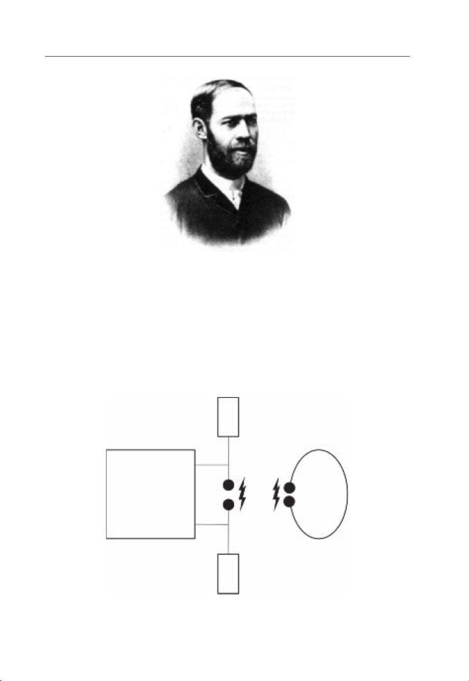
Work onantennasstartedmanyyears ago. The firstwell-knownsatisfactoryantennaexperiment
was conducted by the German physicist Heinrich Rudolf Hertz (1857–1894), pictured in
Figure 1.1. The SI (International Standard) frequency unit, the Hertz, is named after him. In
1887 he built a system, as shown in Figure 1.2, to produce and detect radio waves. The original
intention of his experiment was to demonstrate the existence of electromagnetic radiation.
In the transmitter, a variable voltage source was connected to a dipole (a pair of one-meter
wires) with two conducting balls (capacity spheres) at the ends. The gap between the balls
could be adjusted for circuitresonance as well as forthe generation ofsparks. When the voltage
was increased to a certain value, a spark or break-down discharge was produced. The receiver
was asimple loop with two identical conducting balls. The gap between theballs wascarefully
tuned to receive the spark effectively. He placed the apparatus in a darkened box in order to
see the spark clearly. In his experiment, when a spark was generated at the transmitter, he also
observed a spark at the receiver gap at almost the same time. This proved that the information
from location A (the transmitter) was transmitted to location B (the receiver) in a wireless
manner – by electromagnetic waves.
The information in Hertz’s experiment was actually in binary digital form, by tuning the
spark on andoff.Thiscould be considered theveryfirst digital wireless system,which consisted
of two of the best-known antennas: the dipole and the loop. For this reason, the dipole antenna
is also called the Hertz (dipole) antenna.
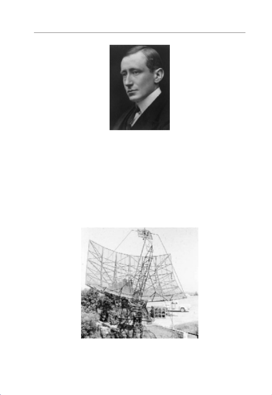
Whilst Heinrich Hertz conducted his experiments in a laboratory and did not quite know
what radio waves might be used for in practice, Guglielmo Marconi (1874–1937, pictured
in Figure 1.3), an Italian inventor, developed and commercialized wireless technology by
introducing a radiotelegraph system, which served as the foundation for the establishment of
numerous affiliated companies worldwide. His most famous experiment was the transatlantic
transmission from Poldhu, UK to St Johns, Newfoundland in Canada in 1901, employing
untuned systems. He shared the 1909 Nobel Prize for Physics with Karl Ferdinand Braun
‘in recognition of their contributions to the development of wireless telegraphy’. Monopole
antennas (near quarter-wavelength) were widely used in Marconi’s experiments; thus vertical
monopole antennas are also called Marconi antennas.
Antennas: From Theory to Practice Yi Huang and Kevin Boyle
C
2008 John Wiley & Sons, Ltd
Page 18
2 Antennas: From Theory to Practice
Figure 1.1 Heinrich Rudolf Hertz
During World War II, battles were won by the side that was first to spot enemy aeroplanes,
ships or submarines. To give the Allies an edge, British and American scientists developed
radar technology to ‘see’ targets from hundreds of miles away, even at night. The research
resulted in the rapid development of high-frequency radar antennas, which were no longer just
wire-type antennas. Some aperture-type antennas, such as reflector and horn antennas, were
developed, an example is shown in Figure 1.4.
Variable
Voltage Source
Figure 1.2 1887 experimental set-up of Hertz’s apparatus
Loop
Page 19
Introduction 3
Figure 1.3 Guglielmo Marconi
Broadband, circularly polarized antennas, as well as many other types, were subsequently
developed for various applications. Since an antenna is an essential device for any radio
broadcasting, communication or radar system, there has always been a requirement for new
and better antennas to suit existing and emerging applications.
More recently, one of the main challenges for antennas has been how to make them broadband and small enough in size for wireless mobile communications systems. For example,
WiMAX (worldwide interoperability for microwave access) is one of the latest systems aimed
at providing high-speed wireless data communications (>10 Mb/s) over long distances from
point-to-point links tofull mobile cellular-typeaccess over a widefrequencyband. The original
WiMAX standard in IEEE 802.16 specified 10 to 66 GHz as the WiMAX band; IEEE 802.16a
Figure 1.4 World War II radar (Reproduced by permission of CSIRO Australia Telescope National
Facility)
Page 20

4 Antennas: From Theory to Practice
was updated in 2004 to 802.16-2004 and added 2 to 11 GHz as an additional frequency range.
The frequency bandwidth is extremely wide although the most likely frequency bands to be
used initially will be around 3.5 GHz, 2.3/2.5 GHz and 5 GHz.
The UWB (ultra-wide band) wireless system is another example of recent broadband radio
communication systems. The allocated frequency band is from 3.1 to 10.6 GHz. The beauty of
the UWB system is that the spectrum, which is normally very expensive, can be used free of
charge but the power spectrum density is limited to −41.3 dBm/MHz. Thus, it is only suitable
for short-distance applications. The antenna design for these systems faces many challenging
issues.
The role of antennas is becoming increasingly important. In some systems, the antenna is
now no longer just a simple transmitting/receiving device, but a device which isintegrated with
other parts of the system to achieve better performance. For example, the MIMO (multiple-in,
multiple-out) antenna system has recently been introduced as an effective means to combat
multipath effects in the radio propagation channel and increase the channel capacity, where
several coordinated antennas are required.
Things have been changing quickly in the wireless world. But one thing has never changed
since the very first antenna was made: the antenna is a practical engineering subject. It will
remain an engineering subject. Once an antenna is designed and made, it must be tested. How
well it works is not just determined by the antenna itself, it also depends on the other parts of
the system and the environment. The standalone antenna performance can be very different
from that of an installed antenna. For example, when a mobile phone antenna is designed, we
must take the case, other parts of the phone and even our hands into account to ensure that it
will work well in the real world. The antenna is an essential device of a radio system, but not
an isolated device! This makes it an interesting and challenging subject.
1.2 Radio Systems and Antennas
A radio system is generally considered to be an electronic system which employs radio waves,
a type of electromagnetic wave up to GHz frequencies. An antenna, as an essential part of a
radio system, is defined as a device which can radiate and receive electromagnetic energy in
an efficient and desired manner. It is normally made of metal, but other materials may also be
used. For example, ceramic materials have been employed to makedielectricresonatorantennas
(DRAs). There are many things in our lives, such as power leads, that can radiate and receive
electromagnetic energy but they cannot be viewed as antennas because the electromagnetic
energy is not transmitted or received in an efficient and desired manner, and because they are
not a part of a radio system.
Since radio systems possess some unique and attractive advantages over wired systems,
numerous radio systems have been developed. TV, radar and mobile radio communication
systems are just some examples. The advantages include:
r
mobility: this is essential for mobile communications;
r
good coverage: the radiation from an antenna can cover a very large area, which is good for
TV and radio broadcasting and mobile communications;
r
low pathloss: this is frequency dependent. Since the loss of a transmission line is an exponential function of the distance (the loss in dB =distance ×per unit loss in dB) and the loss
Page 21
Introduction 5
of a radio wave is proportional to the distance squared (the loss in dB = 20 log10(distance)),
the pathloss of radio waves can be much smaller than that of a cable link. For example,
assume that the loss is 10 dB for both a transmission line and a radio wave over 100 m; if the
distance is now increased to 1000 m, the loss for the transmission line becomes 10 × 10 =
100 dB but the loss for the radio link is just 10 + 20 = 30 dB! This makes the radio link
extremely attractive for long-distance communication. It should be pointed out that optical
fibers are also employed for long-distance communications since they are of very low loss
and ultra-wide bandwidth.
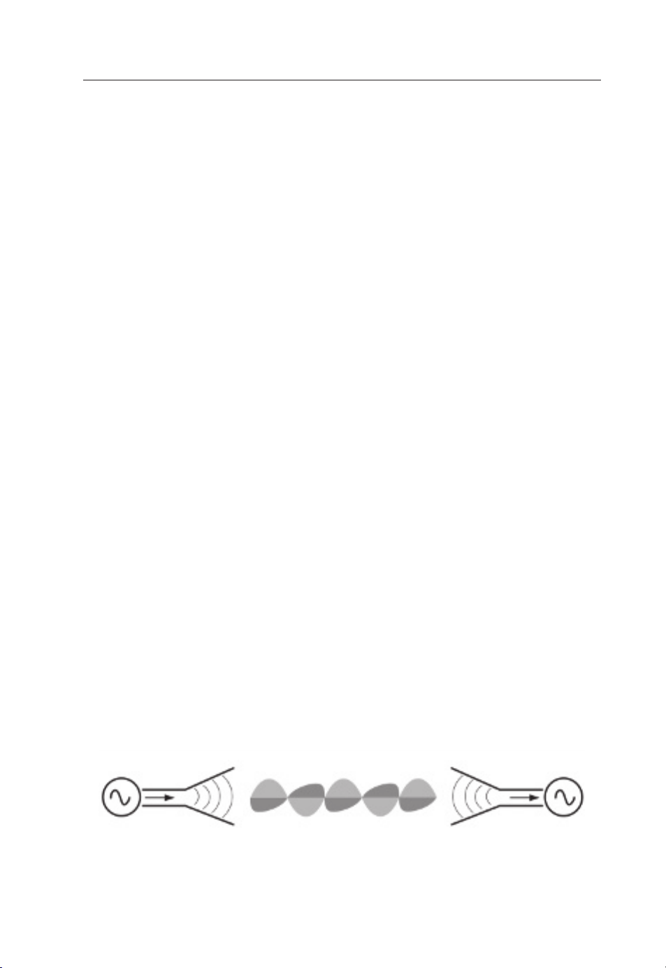
Figure 1.5 illustrates a typical radio communication system. The source information is
normally modulatedand amplified in the transmitter and then passed on to thetransmit antenna
via a transmission line, which has a typical characteristic impedance (explained in the next
chapter) of 50 ohms. The antenna radiates the information in the form of an electromagnetic
wave in an efficient and desired manner to the destination, where the information is picked up
by the receive antenna and passed on to the receiver via another transmission line. The signal
is demodulated and the original message is then recovered at the receiver.
Thus, the antenna is actually a transformer that transforms electrical signals (voltages and
currents from a transmission line) into electromagnetic waves (electric and magnetic fields),
or vice versa. For example, a satellite dish antenna receives the radio wave from a satellite and
transforms it into electrical signalswhich areoutput to a cable tobe further processed. Our eyes
may be viewed as another example of antennas. In this case, the wave is not a radio wave but
an optical wave, another form of electromagnetic wave which has much higher frequencies.
Now it is clear that the antenna is actually a transformer of voltage/current to electric/
magnetic fields, it can also be considered a bridge to link the radio wave and transmission line.
An antennasystem isdefined asthe combinationof theantenna andits feedline. Asan antenna
is usually connected to a transmission line, how to best make this connection is a subject of
interest, since the signal from the feed line should be radiated into the space in an efficient
and desired way. Transmission lines and radio waves are, in fact, two different subjects in
engineering. To understand antenna theory, one has to understand transmission lines and radio
waves, which will be discussed in detail in Chapters 2 and 3 respectively.
In some applications where space is very limited (such as hand-portables and aircraft), it is
desirable to integrate the antenna and its feed line. In other applications (such as the reception
of TV broadcasting), the antenna is far away from the receiver and a long transmission line
has to be used.
Unlike other devices in a radio system (such as filters and amplifiers), the antenna is a very
special device; itdeals with electrical signals (voltages and currents) as well aselectromagnetic
waves (electric fields and magnetic fields), making antenna design an interesting and difficult
Transmission
Transmitter
Line
Antenna
Electromagnetic
wave
Figure 1.5 A typical radio system
Antenna
Receiver
Page 22

6 Antennas: From Theory to Practice
subject. For different applications, the requirements on theantenna may be verydifferent, even
for the same frequency band.
In conclusion, the subject of antennas is about how to design a suitable device which will be
well matched with its feed line and radiate/receive the radio waves in an efficient and desired
manner.
1.3 Necessary Mathematics
To understand antenna theory thoroughly requires a considerable amount of mathematics.
However, the intention of this book is to provide the reader with a solid foundation in antenna
theory andapply the theory to practical antenna design. Here weare justgoing tointroduce and
review the essential and important mathematics required for this book. More in-depth study
materials can be obtained from other references [1, 2].
1.3.1 Complex Numbers
In mathematics, a complex number, Z, consists of real and imaginary parts, that is
Z = R + jX (1.1)
where R is called the real part of the complex number Z , i.e. Re(Z), and X is defined as the
imaginary part of Z , i.e. Im(Z). Both R and X are real numbers and j (not the traditional
notation i in mathematics to avoid confusion with a changing current in electrical engineering)
is the imaginary unit and is defined by
√
j =
−1 (1.2)
Thus
2
j
=−1 (1.3)
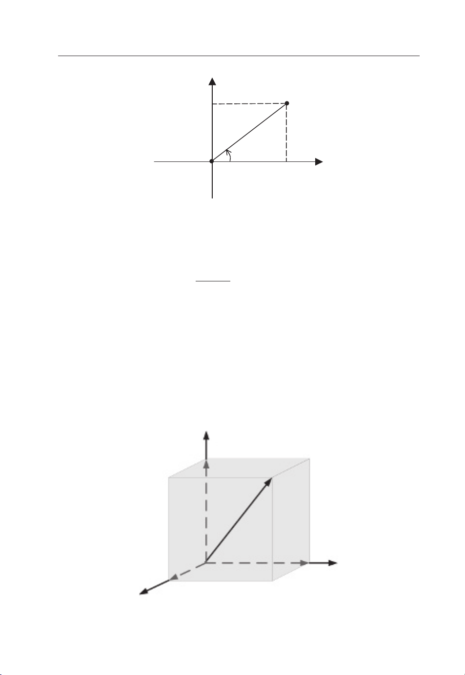
Geometrically, a complex number can be presented in a two-dimensional plane where the
imaginary part is found on the vertical axis whilst the real part is presented by the horizontal
axis, as shown in Figure 1.6.
In this model, multiplication by −1 corresponds to a rotation of 180 degrees about the
origin. Multiplication by j corresponds toa 90-degree rotation anti-clockwise,and the equation
2
j
=−1 is interpreted as saying that if we apply two 90-degree rotations about the origin, the
net resultis asingle 180-degree rotation. Notethat a 90-degree rotation clockwise also satisfies
this interpretation.
Another representation of a complex number Z uses the amplitude and phase form:
Z = Ae
jϕ
(1.4)
Page 23
Introduction 7
jX
Z (R, X)
A
ϕ
R
Figure 1.6 The complex plane
where A is the amplitude and ϕ is the phase of the complex number Z; these are also shown
in Figure 1.6. The two different representations are linked by the following equations:
Z = R + jX = Ae
√
A =
R2+ X2,ϕ= tan−1(X/R)
jϕ
;
(1.5)
R = A cos ϕ, X = A sin ϕ
1.3.2 Vectors and Vector Operation
A scalar is a one-dimensional quantity which has magnitude only, whereas a complex number
is a two-dimensional quantity. A vector can be viewed as a three-dimensional (3D) quantity,
and a special one – it has both a magnitude and a direction. For example, force and velocity
are vectors (whereas speed is a scalar). A position in space is a 3D quantity, but it does not
have a direction, thus it is not a vector. Figure 1.7 is an illustration of vector A in Cartesian
z
A
z
A
A
x
x
Figure 1.7 Vector A in Cartesian coordinates
A
y
y
Page 24
8 Antennas: From Theory to Practice
coordinates. It has three orthogonal components (Ax, Ay, Az) along the x, y and z directions,
respectively. To distinguish vectors from scalars, the letter representing the vector is printed
in bold, for example A or a, and a unit vector is printed in bold with a hat over the letter, for
exampleˆx orˆn.
The magnitude of vector A is given by
2
2
|A|
= A =
A
+ A
x
y
+ A
2
z
(1.6)
Now let us consider two vectors A and B:
ˆ
ˆ
A = A
B = B
x + A
x
ˆ
x + B
x
y
y
y + A
ˆ
y + B
ˆ
z
z
ˆ
z
z
The addition and subtraction of vectors can be expressed as
A + B = (A
A − B = (A
+ Bx)ˆx + (Ay+ By)ˆy + (Az+ Bz)ˆz
x
− Bx)ˆx + (Ay− By)ˆy + (Az− Bz)ˆz
x
(1.7)
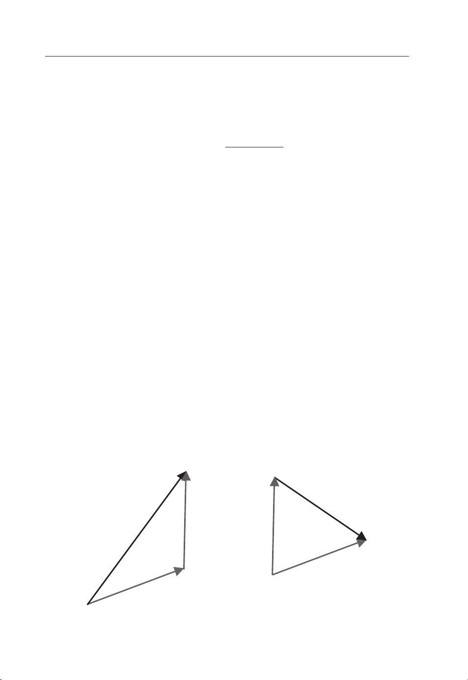
Obviously, the addition obeys the commutative law, that is A + B = B + A.
Figure 1.8 shows what the addition and subtraction mean geometrically. A vector may
be multiplied or divided by a scalar. The magnitude changes but its direction remains the
same. However, the multiplication of two vectors is complicated. There are two types of
multiplication: the dot product and the cross product.
The dot product of two vectors is defined as
ArB =|A||B|cos θ = A
+ AyBy+ AzB
xBx
z
(1.8)
where θ is the angle between vector A and vector B and cos θ is also called the direction
cosine. The dotrbetween A and B indicates the dot product, which results in a scalar; thus, it
is also called a scalar product. If the angle θ is zero, A and B are in parallel – thedot product is
A–B
A+B
B
B
A
Figure 1.8 Vector addition and subtraction
A
Page 25
Introduction 9
C
Right-Hand
Rule
B
A
Figure 1.9 The cross product of vectors A and B
maximized – whereas for an angle of 90 degrees, i.e. when A and B are orthogonal, the dot
product is zero.
It is worth noting that the dot product obeys the commutative law, that is, ArB = BrA.
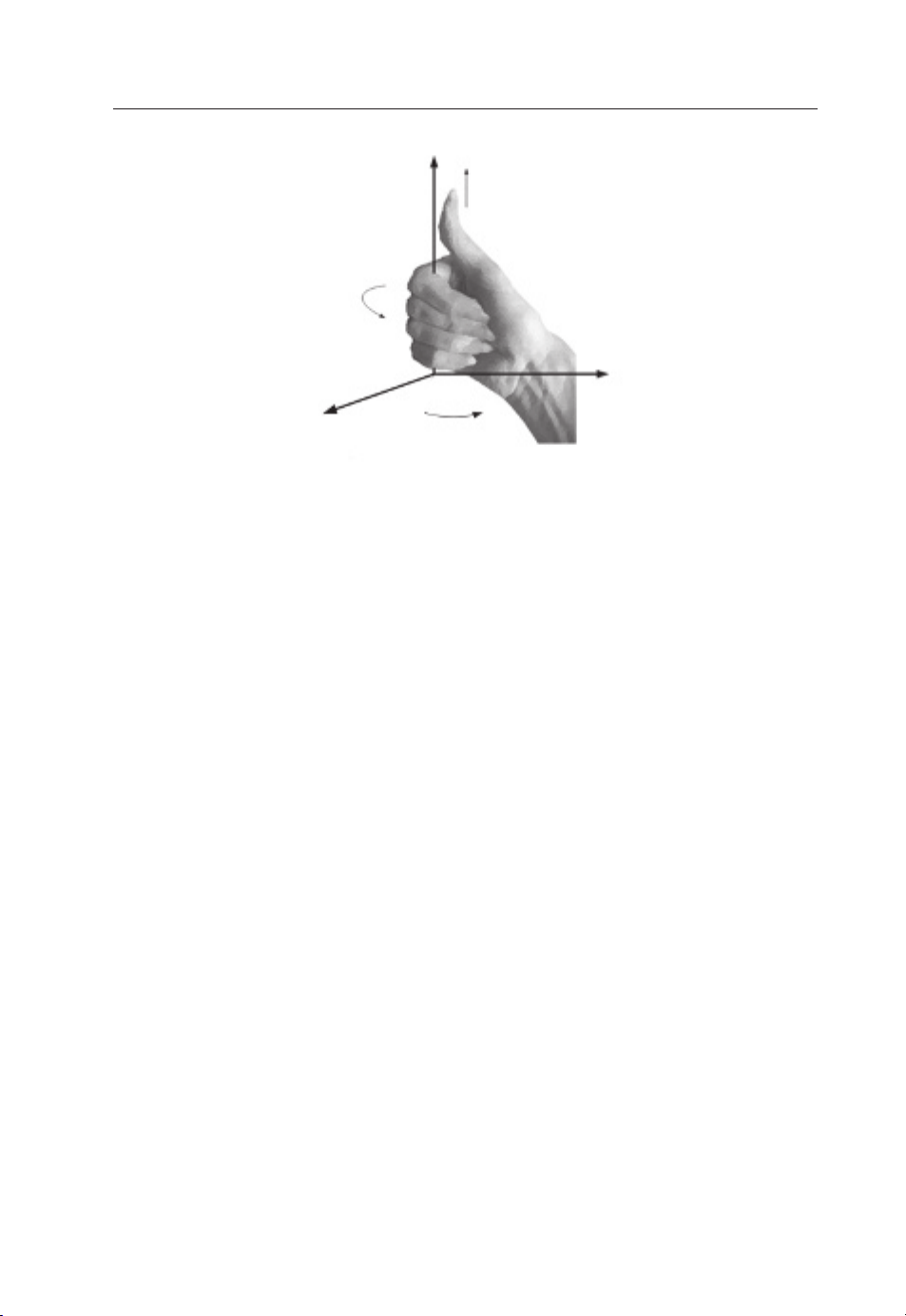
The cross product of two vectors is defined as
A × B =ˆn|A||B|sin θ = C
=ˆx(A
− AzBy) +ˆy( AzBx− AxBz) +ˆz( AxBy− AyBx)
yBz
(1.9)
whereˆn is a unit vector normal to the plane containing A and B. The cross × between A
and B indicates the cross product, which results in a vector C; thus, it is also called a vector
product. The vector C is orthogonal to both A and B, and the direction of C follows a so-called
right-hand rule, as shown in Figure 1.9. If the angle θ is zero or 180 degrees, that is, A and B
are in parallel, the cross product is zero; whereas for an angle of 90 degrees, i.e. A and B are
orthogonal, the cross product of these two vectors reaches a maximum.Unlike the dot product,
the cross product does not obey the commutative law.
The cross product may be expressed in determinant form as follows, which is the same as
Equation (1.9) but may be easier for some people to memorize:
A × B =
ˆ
xˆy
A
AyA
x
BxByB
ˆ
z
z
z
(1.10)
Another important thing about vectors is that any vector can be decomposed into three
orthogonal components (such as x, y and z components) in 3D or two orthogonal components
in a 2D plane.
Example 1.1: Vector operation. Given vectors A = 10
ˆ
x + 5ˆy + 1ˆz and B = 2ˆy, find:
A + B; A − B; A • B; and A × B
Page 26
10 Antennas: From Theory to Practice
x
Solution:
A + B = 10ˆx + (5 +2)ˆy + 1ˆz = 10ˆx + 7ˆy + 1ˆz;
A − B = 10ˆx + (5 −2)ˆy + 1ˆz = 10ˆx + 3ˆy + 1ˆz;
A • B = 0 +(5 ×2) + 0 = 10;
A × B = 10 ×2ˆz + 1 × 2ˆx = 20ˆz + 2ˆx
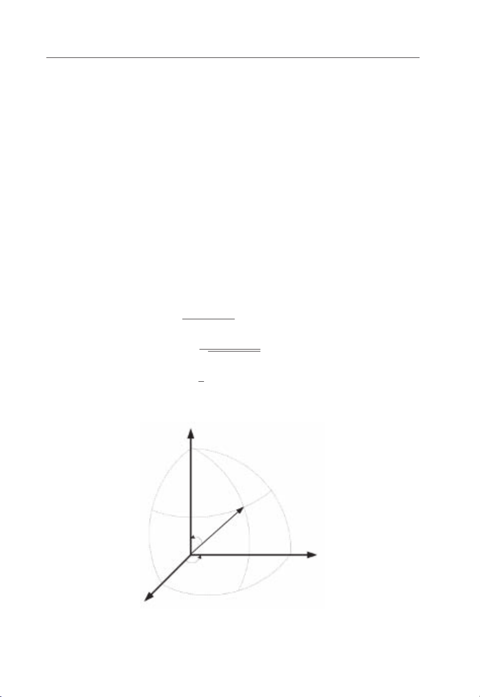
1.3.3 Coordinates
In addition to the well-known Cartesian coordinates, spherical coordinates (r, θ,φ), as shown
in Figure 1.10,will also be used frequentlythroughout this book.These two coordinatesystems
have the following relations:
x = r sin θ cosφ
y = r sin θ sinφ
z = r cos θ
and
(1.11)
r =
θ = cos
φ = tan
x2+ y2+ z
−1
x2+ y2+ z
y
−1
;0≤ φ ≤ 2π
x
z
θ
r
φ
2
z
;0≤ θ ≤ π (1.12)
2
P
y
Figure 1.10 Cartesian and spherical coordinates
Page 27

Introduction 11
The dot products of unit vectors in these two coordinate systems are:
r
ˆ
ˆ
x
r = sin θ cosφ;ˆy
r
ˆ
ˆ
x
θ = cos θ cos φ;ˆy
r
ˆ
ˆ
x
φ =−sin φ;ˆy
r
ˆ
r = sin θ sinφ;ˆz
r
ˆ
θ = cos θ sin φ;ˆz
r
ˆ
φ = cosφ;ˆz
r
ˆ
φ = 0
r
ˆ
r = cos θ
r
ˆ
θ =−sin θ
(1.13)
Thus, we can express a quantity in one coordinate system using the known parameters in the
other coordinate system. For example, if A
r
A
x
ˆ
= A
x = Arsin θ cosφ + Aθcos θ cosφ − Aφsin φ
, Aθ, Aφare known, we can find
r
1.4 Basics of Electromagnetics
Now let us use basic mathematics to deal with antennas or, more precisely, electromagnetic
(EM) problems in this section.
EM waves cover the whole spectrum; radio waves and optical waves are just two examples
of EM waves. We can see light but we cannot see radio waves. The whole spectrum is divided
into many frequency bands. Some radio frequency bands are listed in Table 1.1.
Although the whole spectrum is infinite, the useful spectrum is limited and some frequency
bands, such as the UHF, are already very congested. Normally, significant license fees have to
be paid to use the spectrum, although there are some license-free bands: the most well-known
ones are the industrial, science and medical (ISM) bands. The 433 MHz and 2.45 GHz are just
two examples. Cable operators do not need to pay the spectrum license fees, but they have to
pay other fees for things such as digging out the roads to bury the cables.
The wave velocity, v, is linked to the frequency, f , and wavelength, λ, by this simple
equation:
λ
v =
f
It is well known that the speed of light (an EM wave) is about 3 ×10
8
m/s in free space. The
(1.14)
higher the frequency,the shorter the wavelength. An illustration of how the frequency is linked
Table 1.1 EM spectrum and applications
Frequency Band Wavelength Applications
3–30 kHz VLF 100–10 km Navigation, sonar, fax
30–300 kHz LF 10–1 km Navigation
0.3–3 MHz MF 1–0.1 km AM broadcasting
3–30 MHz HF 100–10 m Tel, fax, CB, ship communications
30–300 MHz VHF 10–1 m TV, FM broadcasting
0.3–3 GHz UHF 1–0.1 m TV, mobile, radar
3–30 GHz SHF 100–10 mm Radar, satellite, mobile, microwave links
30–300 GHz EHF 10–1 mm Radar, wireless communications
0.3–3 THz THz 1–0.1 mm THz imaging
Page 28
12 Antennas: From Theory to Practice
8
10
6
10
4
10
2
10
0
10
-2
10
Wavelength (m)
-4
10
-6
10
-8
10
-10
10
0 102 104 106 108 1010 1012 1014 1016
10
Optical
Communications
(1.7μm−0.8μm)
Conventional RF
1Hz−300MHz/1GHz
Microwave
300MHz−30GHz
(1m−1cm)
Millimeter Wave
30GHz−300GHz
Light
(0.76μm−0.4μm)
Frequency (Hz)
Figure 1.11 Frequency vs wavelength
to the wavelength is given in Figure 1.11, where both the frequency and wavelength are plotted
on a logarithmic scale. The advantage of doing this is that we can see clearly how the function
is changed, even over a very large scale.
Logarithmic scales are widely used in RF (radio frequency) engineering and the antennas
community since the signals we are dealing with change significantly (over 1000 times in
many cases) in terms of the magnitude. The signal power is normally expressed in dB and is
defined as
P(dBW) = 10log
10
P(W)
; P(dBm) = 10 log
1W
10
P(W)
1mW
(1.15)
Thus, 100 watts is 20 dBW, just expressed as 20 dB in most cases. 1 W is 0 dB or 30 dBm
and 0.5 W is −3 dB or 27 dBm. Based on this definition, we can also express other parameters
in dB. For example, since the power is linked to voltage V by P = V
2
R (so P ∝ V
2
), the
voltage can be converted to dBV by
V (dBV) = 20log
10
V (V )
1V
(1.16)
Thus, 3 kVolts is 70 dBV and 0.5 Volts is –6 dBV (not −3 dBV) or 54 dBmV.
1.4.1 The Electric Field
The electric field (in V/m) is defined as the force (in Newtons) per unit charge (in Coulombs).
From this definition and Coulomb’s law, the electric field, E, created by a single point
Page 29

Introduction 13
charge Q at a distance r is
F
E =
Q
where
F is the electric force given by Coulomb’s law (F =
ˆ
ris a unit vector along the r direction, which is also the direction of the electric field E;
=
Q
ˆ
r (V /m) (1.17)
2
4πεr
Q1Q
2
ˆ
r);
2
4πεr
ε is the electricpermittivity (it is also calledthe dielectric constant,but is normallya function
of frequency and not really a constant, thus permittivity is preferred in this book) of the
material. Its SI unit is Farads/m. In free space, it is a constant:
ε
= 8.85419 × 10
0
−12
F/m (1.18)
The product of the permittivity and the electric field is called the electric flux density, D,
which is a measure of how much electric flux passes through a unit area, i.e.
where ε
D = εE = ε
= ε/ε0is called the relative permittivity or relative dielectric constant. The relative
r
E(C/m2) (1.19)
rε0
permittivities of some common materials are listed in Table 1.2. Note that they are functions
of frequency and temperature. Normally, the higher the frequency, the smaller the permittivity
in the radio frequency band. It should also be pointed out that almost all conductors have a
relative permittivity of one.
The electric flux density is also called the electric displacement, hence the symbol D.Itis
also a vector. In an isotropic material (properties independent of direction), D and E are in
the same direction and ε is a scalar quantity. In an anisotropic material, D and E may be in
different directions if ε is a tensor.
If the permittivity isa complex number, it meansthatthe material hassome loss. The complex
permittivity can be written as
− j ε
(1.20)
ε = ε
The ratio of the imaginary part to the real part is called the loss tangent, that is
tan δ =
ε
ε
(1.21)
It has no unit and is also a function of frequency and temperature.
The electric field E is related to thecurrent density J (in A/m
2
), another importantparameter,
by Ohm’s law. The relationship between them at a point can be expressed as
J = σ E (1.22)
where σ is the conductivity, which is the reciprocal of resistivity. It is a measure of a material’s
ability to conduct an electrical current and is expressed in Siemens per meter (S/m). Table 1.3
Page 30

14 Antennas: From Theory to Practice
Table 1.2 Relative permittivity of some common materials at 100 MHz
Material Relative permittivity Material Relative permittivity
ABS (plastic) 2.4–3.8 Polypropylene 2.2
Air 1 Polyvinylchloride (PVC) 3
Alumina 9.8 Porcelain 5.1–5.9
Aluminum silicate 5.3–5.5 PTFE-teflon 2.1
Balsa wood 1.37 @ 1 MHz PTFE-ceramic 10.2
1.22 @ 3 GHz
Concrete ∼8 PTFE-glass 2.1–2.55
Copper 1 RT/Duroid 5870 2.33
Diamond 5.5–10 RT/Duroid 6006 6.15@3GHz
Epoxy (FR4) 4.4 Rubber 3.0–4.0
Epoxy glass PCB 5.2 Sapphire 9.4
Ethyl alcohol (absolute) 24.5 @ 1 MHz Sea water 80
6.5 @ 3 GHz
FR-4(G-10)
–low resin 4.9 Silicon 11.7–12.9
–high resin 4.2
GaAs 13.0 Soil ∼10
Glass ∼4 Soil (dry sandy) 2.59@1MHz
2.55 @ 3 GHz
Gold 1 Water (32
(68
(212
◦
F) 88.0
◦
F) 80.4
◦
F) 55.3
Ice (pure distilled water) 4.15 @ 1 MHz Wood ∼2
3.2 @ 3 GHz
Table 1.3 Conductivities of some common materials at room temperature
Material Conductivity (S/m) Material Conductivity (S/m)
Silver 6.3 ×10
Copper 5.8 × 10
Gold 4.1 ×10
Aluminum 3.5 ×10
Tungsten 1.8 ×10
Zinc 1.7 × 10
Brass 1 ×10
Phosphor bronze 1 ×10
Tin 9 × 10
Lead 5 ×10
Silicon steel 2 ×10
Stainless steel 1 × 10
Mercury 1 ×10
Cast iron ≈ 10
7
7
7
7
7
7
7
7
6
6
6
6
6
6
Graphite ≈ 10
Carbon ≈ 10
Silicon ≈ 10
Ferrite ≈ 10
Sea water ≈ 5
Germanium ≈ 2
Wet soil ≈ 1
Animal blood 0.7
Animal body 0.3
Fresh water ≈ 10
Dry soil ≈ 10
Distilled water ≈ 10
Glass ≈ 10
Air 0
5
4
3
2
−2
−3
−4
−12
Page 31

Introduction 15
lists conductivities of some commonmaterials linked to antenna engineering. The conductivity
is also a function of temperature and frequency.
1.4.2 The Magnetic Field
Whilst charges can generate an electric field, currents can generate a magnetic field. The
magnetic field, H (in A/m),is the vector field which formsclosed loops aroundelectric currents
or magnets. The magnetic field from a current vector I is given by the Biot–Savart law as
I ׈r
H =
where
ˆ
r is the unit displacement vector from the current element to the field point and
r is the distance from the current element to the field point.
I,ˆr and H follow the right-hand rule; that is, H is orthogonal to both I andˆr, as illustrated
by Figure 1.12.
Like the electric field, the magnetic field exerts a force on electric charge. But unlike an
electric field, it employs force only on a moving charge, and the direction of the force is
orthogonal to both the magnetic field and the charge’s velocity:
(A/m) (1.23)
2
4πr
F = Qv × μH (1.24)
where
F is the force vector produced, measured in Newtons;
Q is the electric charge that the magnetic field is acting on, measured in Coulombs (C);
v is the velocity vector of the electric charge Q, measured in meters per second (m/s);
μ is the magnetic permeability of the material. Its unit is Henries per meter (H/m). In free
space, the permeability is
μ
= 4π ×10−7H/m (1.25)
0
In Equation (1.24), Qv can actually be viewed as the current vector I and the product of
μH is called the magnetic flux density B (in Tesla), the counterpart of the electric flux density.
I
H
r
Figure 1.12 Magnetic field generated by current I
Page 32

16 Antennas: From Theory to Practice
Table 1.4 Relative permeabilities of some common materials
Material Relative permeability Material Relative permeability
Superalloy ≈ 1 × 10
Purified iron ≈ 2 × 10
Silicon iron ≈ 7 × 10
Iron ≈ 5 ×10
Mild steel ≈ 2 × 10
Nickel 600 Silver ≈1
6
5
3
3
3
Aluminum ≈1
Air 1
Water ≈1
Copper ≈1
Lead ≈1
Thus
B = μH (1.26)
Again, in an isotropic material (properties independent of direction), B and H are in the same
direction and μ is a scalar quantity. In an anisotropic material, B and E may be in different
directions and μ is a tensor.
Like the relative permittivity, the relative permeability is given as
μ
= μ/μ
r
0
(1.27)
The relative permeabilities of some materials are given in Table 1.4. Permeability is not
sensitive to frequency or temperature. Most materials, including conductors, have a relative
permeability very close to one.
Combining Equations (1.17) and (1.24) yields
F = Q(E + v × μH) (1.28)
This is called the Lorentz force. The particle will experience a force due to the electric field
QE, and the magnetic field Qv × B.
1.4.3 Maxwell’s Equations
Maxwell’s equations are a set of equations first presented as a distinct group in the latter
half of the nineteenth century by James Clerk Maxwell (1831–1879), pictured in Figure 1.13.
Mathematically they can be expressed in the following differential form:
d B
dt
d D
dt
(1.29)
where
ρ is the charge density;
∂
∂
ˆ
∇=
∂x
x +
ˆ
y +
∂y
∇×E =−
∇×H = J +
∇rD = ρ
∇rB = 0
∂
ˆ
z is a vector operator;
∂z
Page 33

Introduction 17
Figure 1.13 James Clerk Maxwell
∇×is the curl operator, called rot in some countries instead of curl;
∇ris the divergence operator.
Here we have both the vector cross product and dot product.
Maxwell’s equations describe the interrelationship between electric fields, magnetic fields,
electric charge and electric current. Although Maxwell himself was not the originator of the
individual equations, he derived them again independently in conjunction with his molecular
vortex model of Faraday’s lines of force, and he was the person who first grouped these equations together into a coherent set. Most importantly, he introduced an extra term to Ampere’s
Circuital Law, the second equation of (1.19). This extra term is the time derivative of the
electric field and is known as Maxwell’s displacement current. Maxwell’s modified version
of Ampere’s Circuital Law enables the set of equations to be combined together to derive the
electromagnetic wave equation, which will be further discussed in Chapter 3.
Now let us have a closer look at these mathematical equations to see what they really mean
in terms of the physical explanations.
1.4.3.1 Faraday’s Law of Induction
∇×E =
dB
dt
(1.30)
This equation simply means that the induced electromotive force is proportional to the rate of
change of the magnetic flux through a coil. In layman’s terms, moving a conductor (such as
a metal wire) through a magnetic field produces a voltage. The resulting voltage is directly
proportional to the speed of movement. It is apparent from this equation that a time-varying
magnetic field (μ
d H
= 0) will generate an electric field, i.e. E = 0. But if the magnetic field
dt
is not time-varying, it will NOT generate an electric field.
Page 34

18 Antennas: From Theory to Practice
1.4.3.2 Ampere’s Circuital Law
∇×H = J +
This equation was modified by Maxwell by introducing the displacement current
dD
dt
d D
. It means
dt
(1.31)
that a magnetic field appears during the charge or discharge of a capacitor. With this concept,
and Faraday’s law, Maxwell was able to derive the wave equations, and by showing that the
predicted wave velocity was the same as the measured velocity of light, Maxwell asserted that
light waves are electromagnetic waves.
This equation shows that both the current (J) and time-varying electric field (ε
d E
dt
) can
generate a magnetic field, i.e. H = 0.
1.4.3.3 Gauss’s Law for Electric Fields
∇rD = ρ (1.32)
This is the electrostatic application of Gauss’s generalized theorem, giving the equivalence
relation between any flux, e.g. of liquids, electric or gravitational, flowing out of any closed
surface and the result of inner sources and sinks, such as electric charges or masses enclosed
within the closed surface. As a result, it is not possible for electric fields to form a closed loop.
Since D = εE, it is also clear that charges (ρ) can generate electric fields, i.e. E = 0.
1.4.3.4 Gauss’s Law for Magnetic Fields
∇rB = 0 (1.33)
This shows that the divergence of the magnetic field (∇rB) is always zero, which means that
the magnetic field lines are closed loops; thus, the integral of B over a closed surface is zero.
For atime-harmonic electromagnetic field (which means a fieldlinked to time by factor e
jωt
where ω is the angular frequency and t is the time), we can use the constitutive relations
D = εE, B = μH, J = σ E (1.34)
to write Maxwell’s equations in the following form
∇×E =−jωμH
∇×H = J + j ωεE = jωε1 − j
σ
ωε
E
(1.35)
∇rE = ρ/ε
∇rH = 0
where B and D are replaced by the electric field E and magnetic field H to simplify the
equations and they will not appear again unless necessary.
Page 35

Introduction 19
It should be pointed out that, in Equation (1.35), ε(1 − j
σ
) can be viewed as a complex
ωε
permittivity defined by Equation (1.20). In this case, the loss tangent is
ε
tan δ =
σ
=
ε
ωε
(1.36)
It is hard to predict how the loss tangent changes with the frequency, since both the permittivity and conductivity are functions of frequency as well. More discussion will be given in
Chapter 3.
1.4.4 Boundary Conditions
Maxwell’s equations can also be written in the integral form as
Erdl =−
C
Hrdl =
C
Drds =
S
Brds = 0
S
S
V
S
(J +
d B
r
ds
dt
d D
)rds
dt
ρdv = Q
(1.37)
Consider the boundary between two materials shown in Figure 1.14. Using these equations,
we can obtain a number of useful results. For example, if we apply the first equation of
Maxwell’s equations in integral form to the boundary between Medium 1 and Medium 2, it is
not difficult to obtain [2]:
ˆ
n × E
=ˆn × E
1
2
(1.38)
whereˆn is the surface unit vector from Medium 2 to Medium 1, as shown in Figure 1.14. This
condition means that the tangential components of an electric field (ˆn × E) are continuous
across the boundary between any two media.
ε
Medium 1
Medium 2
Figure 1.14 Boundary between Medium 1 and Medium 2
ˆ
n
, σ1, μ
1
ε2, σ2, μ
1
2
Page 36

20 Antennas: From Theory to Practice
1
+
Figure 1.15 Electromagnetic field distribution around a two-wire transmission line
V
E
H
2
−
Similarly, we can apply the other three Maxwell equations to this boundary to obtain:
ˆ
where J
n ×(H
ˆ
nr(ε
ˆ
nr(μ
is the surface current density and ρsis the surface charge density. These results can
s
− H2) = J
1
− ε2E2) = ρ
1E1
− μ2H2) = 0
1H1
s
s
be interpreted as
r
the change in tangential component of the magnetic field across a boundary is equal to the
surface current density on the boundary;
r
the change in the normal component of the electric flux density across a boundary is equal
to the surface charge density on the boundary;
r
the normal component of the magneticfluxdensityiscontinuousacrossthe boundary between
two media, whilst the normal component of the magnetic field is not continuous unless
μ
= μ2.
1
(1.39)
Applying these boundary conditions on a perfect conductor (which means no electric and
magnetic field inside and the conductivity σ =∞)intheair,wehave
ˆ
n × E = 0;ˆn × H = J
;ˆnrE = ρs/ε;ˆnrH = 0 (1.40)
s
We can also use these results to illustrate, for example, the field distribution around a twowire transmission line, as shown in Figure 1.15, where the electric fields are plotted as the
solid lines and the magnetic fields are shown as broken lines. As expected, the electric field
is from positive charges to negative charges, whilst the magnetic field forms loops around the
current.
Page 37

Introduction 21
1.5 Summary
In this chapter we have introduced the concept of antennas, briefly reviewed antenna history
and laiddown the mathematical foundations for further study. The focushas been on the basics
of electromagnetics, which include electric and magnetic fields, electromagnetic properties of
materials, Maxwell’s equations and boundary conditions. Maxwell’s equations have revealed
how electric fields, magnetic fields and sources (currents and charges) are interlinked. They
are the foundation of electromagnetics and antennas.
References
[1] R. E. Collin, Antennas and Radiowave Propagation, McGraw-Hill, Inc., 1985.
[2] J. D. Kraus and D. A. Fleisch, Electromagnetics with Applications, 5th edition, McGraw-Hill, Inc., 1999.
Problems
Q1.1 What wireless communication experiment did H. Hertz conduct in 1887? Use a
diagram to illustrate your answer.
Q1.2 Use an example to explain what a complex number means in our daily life.
Q1.3 Given vectors A = 10ˆx +5ˆy + 1ˆz and B = 5ˆz, find
a. the amplitude of vector A;
b. the angle between vectors A and B;
c. the dot product of these two vectors;
d. a vector which is orthogonal to A and B.
Q1.4 Given vector A = 10sin(10t + 10z)ˆx + 5ˆy, find
Q1.5 Vector E = 10e
Q1.6 Explain why mobile phone service providers have to pay license fees to use the
Q1.7 Cellular mobile communications have become part of our daily life. Explain the
Q1.8 Which frequency bands have been used for radar applications? Give an example.
Q1.9 Express 1 kW in dB, 10 kV in dBV, 0.5 dB in W and 40 dBμV/m in V/m and
Q1.10 Explain the concepts of the electric field and magnetic field. How are they linked
r
a. ∇
A;
b. ∇×A;
r
c. (∇
∇) A;
r
d. ∇∇
a. find the amplitude of E;
b. plot the real part of E as a function of t ;
c. plot the real part of E as a function of z;
d. explain what this vector means.
spectrum. Who is responsible for the spectrum allocation in your country?
major differences between the 1st, 2nd and 3rd generations of cellular mobile
systems in terms of the frequency, data rate and bandwidth. Further explain why
their operational frequencies have increased.
μV/m.
to the electric and magnetic flux density functions?
A
j (10t−10z)
ˆx.
Page 38

22 Antennas: From Theory to Practice
Q1.11 What are the material properties of interest to our electromagnetic and antenna
engineers?
Q1.12 What is the Lorentz force? Name an application of the Lorentz force in our daily
life.
Q1.13 If a magnetic field on a perfect conducting surface z = 0isH = 10cos(10t − 5z)ˆx,
find the surface current density J
.
s
Q1.14 Use Maxwell’s equations to explain the major differences betweenstatic EM fields
and time-varying EM fields.
Q1.15 Express the boundary conditions for the electric and magnetic fields on the surface
of a perfect conductor.
Page 39

2
Circuit Concepts and Transmission Lines
In this chapter we are going to review the very basics of circuit concepts and distinguish
the lumped element system from the distributed element system. The focus will be on the
fundamentals of transmission lines, including the basic model, the characteristic impedance,
input impedance, reflection coefficient,return loss and voltagestanding wave ratio (VSWR) of
a transmission line. The SmithChart, impedance-matching techniques,Q factor andbandwidth
will also be addressed. A comparison of various transmission lines and associated connectors
will be made at the end of this chapter.
2.1 Circuit Concepts
Figure 2.1 shows a very basic electrical circuit where a voltage source V is connected to a
load Z via conducting wires. This simple circuit can represent numerous systems in our daily
life, from a simple torch – a DC (direct current) circuit – to a more complicated power supply
system – an AC (alternating current) circuit. To analyze such a circuit, one has to use the
following four quantities:
r
Electric current I is a measure of the charge flow/movement. The SI unit of current is the
Ampere (A), which is equal to a flow of one Coulomb of charge per second.
r
Voltage V is the difference in electrical potential between two points of an electrical or
electronic circuit. The SI unit of voltage is the Volt (V). Voltage measures the potential
energy of an electric field to cause an electric current in a circuit.
r
Impedance Z = R + jX is a measure of opposition to an electric current. In general, the
impedance is a complex number, its real part R is the electrical resistance (or just resistance)
and reflects the ability to consume energy, whilst the imaginary part X is the reactance
and indicates the ability to store energy. If the reactance is positive, it is called inductance
since the reactance of an inductor is positive (ωL); if the reactance is negative, it is then
Antennas: From Theory to Practice Yi Huang and Kevin Boyle
C
2008 John Wiley & Sons, Ltd
Page 40

24 Antennas: From Theory to Practice
Z
V
Figure 2.1 A simple electrical circuit with a source and load
called capacitance since the reactance of a capacitor is negative (−1/ωC). The same unit,
the Ohm (),is used forimpedance, resistance and reactance. The inverses of the impedance,
resistance and reactance are called the admittance (Y ), conductance (G) and susceptance
(B), respectively. Their unit is the Siemens (S) and it is 1 Ohm.
r
Power P is defined as the amount of work done by an electrical current, or the rate at which
electrical energy is transmitted/consumed. The SI unit of power is the Watt (W). When an
electric current flows through a device with resistance, the device converts the power into
various forms, such as light (light bulbs), heat (electric cooker), motion (electric razor),
sound (loudspeaker) or radiation for an antenna.
Ohm’s law is the fundamental theory for electrical circuits. It reveals how the current,
voltage and resistance are linked in a DC circuit. It states that the current passing through a
conductor/device from one terminal point on the conductor/device to another terminal point
on the conductor/device is directly proportional to the potential difference (i.e. voltage) across
the two terminal points and inversely proportional to the resistance of the conductor/device
between the two terminal points. That is
V
I =
R
(2.1)
In an AC circuit, Ohm’s law can be generalized as
V
I =
Z
(2.2)
i.e. the resistance R is replaced by the impedance Z. Since the impedance is acomplex number,
both the current and voltage can be complex numbers as well, which means that they have
magnitude and phase.
The average power can be obtained using
2
/R = RI2for DC (2.3)
2
V
1
I
0V0
0
=
2R
2
RI
0
for AC
=
2
where V
P = IV = V
1
P
=
av
2
and I0are the amplitudes of voltage and current, respectively.
0
Page 41

Circuit Concepts and Transmission Lines 25
2.1.1 Lumped and Distributed Element Systems
In traditional circuit theory,we basically divide circuits into thosethat are DCand those that are
AC. The voltage, current and impedance are real numbers in DC circuits but complex numbers
in AC circuits. The effects of conducting wires can normally be neglected. For example, the
current across the load Z in Figure 2.1 can be obtained usingOhm’slaw. It is given by Equation
(2.2) and considered to be the same voltage across the load.
In most countries, the electrical power supply system operates at 50 or 60 Hz, which means
a wavelength of 6000 or 5000 km (close to the radius of the Earth: 6378 km), much longer
than any transmission line in use. The current and voltage along the transmission line may
be considered unchanged. The system is called a lumped element system. However, in some
applications the frequency of the source is significantly increased, as a result the wavelength
becomes comparable with the length of the transmission line linking the source and the load.
The current and voltage along the transmission line are functions of the distance from the
source, thus the system is called a distributed element system. If Figure 2.1 is a distributed
element system, Equation (2.2) is no longer valid since the voltage across the load may now be
very different from the source voltage. V
the load.
Conventional circuit theory was developed for lumped element systems whose frequency
is relatively low and where the wavelength is relatively large. However, the frequency of
a distributed system is relatively high and the wavelength is relatively short. It is therefore
important to introduce the transmissionlinetheory, which has beendeveloped forthedistributed
element system and hastakenthedistributednatureof the parameters in thesystemintoaccount.
should therefore be replaced by the voltage across
0
2.2 Transmission Line Theory
A transmission line is the structure that forms all or part of a path from one place to another
for directing the transmission of energy, such as electrical power transmission and optical
waves.Examples of transmissionlinesinclude conducting wires,electrical power lines, coaxial
cables, dielectricslabs, opticalfibers andwaveguides.In thisbook weare onlyinterested inthe
transmission lines for RF engineering and antenna applications. Thus, dielectric transmission
lines such as optical fibers are not considered.
2.2.1 Transmission Line Model
The simplest transmission line is a two-wire conducting transmission line, as shown in Figure
2.2. It has been widely used for electrical power supply and also for radio and television
systems. In the old days, the broadcasting TV signal was received by an antenna and then
passed down to a TV via such a two-wire conducting wire, which has now been replaced by
the coaxial cable. This is partially due to the fact that the antenna used now (the Yagi–Uda
antenna, a popular TV antenna to be discussed in Chapter 5, which has an input impedance
around 75 ohms) is different from the antenna used then (the folded dipole, which was a
popular TV antenna many years ago and had an input impedance around 300 ohms). Also, the
coaxial cable performs much better than the two-wire transmission line at the UHF (ultra-high
frequency) TV bands.
Page 42

26 Antennas: From Theory to Practice
z
z + Δz
z
1
2
I(z
R
L
1
1
I(z)
1
1
L
R
+ Δz)
L
R
1
1
1
G
C
V(z)
G
C
V(z + Δz)
G
C
2
R
L
2
2
R
L
2
2
z
R
z + Δ z
L
2
2
Figure 2.2 A two-wire transmission line model
As shown in Figure 2.2, if we divide the transmission line into many (almost infinite) short
segmentsof length z, which is muchsmallerthan the wavelength of interest,eachsegmentcan
then be represented using a set oflumped elements.By doing so, a distributedtransmission line
is modeled as an infinite series of two-port lumped elementary components, each representing
an infinitesimally short segment of the transmission line. To make the analysis easier, the
equivalent circuit of the segment of the transmission line is simplified to Figure 2.3, where
R = R
+ R2and L = L1+ L2.
1
r
The resistance R represents the conductive loss of the transmission line over a unit length,
thus the unit is ohms/unit length (/m).
r
The inductance L is the self-inductance of the transmission line and is expressed in Henries
per unit length (H/m).
r
The capacitance C between the two conductors is represented by a shunt capacitor with a
unit of Farads per unit length (F/m).
r
The conductance G of the dielectric material separating the two conductors is represented
by a conductance G shunted between the two conductors. Its unit is Siemens per unit length
(S/m).
R
I(z)
V(z)
L
G
C
Figure 2.3 Schematic representation of the elementary component of a transmission line
I(z
V(z
Δz)
Δz)
Page 43

Circuit Concepts and Transmission Lines 27
It should be repeated for clarity that the model consists of an infinite series of elements
shown in Figure 2.3, and that the values of the components are specified per unit length. R, L,
C and G may be functions of frequency.
Using this model we are going to investigate how the current and voltage along the line are
changed and how they are linked to R, L, C and G.
It is reasonable to assume that the source is time-harmonic and has an angular frequency
ω(= 2π f, where f is the frequency), thus its time factor is e
jωt
.
Using Ohm’s law, we know that the voltage drop and current change over a segment of z
can be expressed in the frequency domain as:
V (z + z) − V (z) =−(R + j ωL)z · I(z)
(2.4)
I(z + z) − I (z) =−(G + j ωC)z · V(z + z)
When z approaches zero, these two equations can be written in differential form as:
dV(z)
=−(R + j ωL) · I(z)
dz
dI(z)
=−(G + jωC) ·V (z)
dz
(2.5)
Differentiating with respect to z on both sides of the equations and combining them gives:
2
d
V (z)
= (R + j ωL)(G + jωC) · V(z)
2
dz
2
d
I(z)
= (R + j ωL)(G + jωC) · I(z)
2
dz
(2.6)
That is,
2
d
V (z)
− γ2V (z) = 0
2
d
dz
2
dz
I(z)
2
− γ2I(z) = 0
(2.7)
where
γ =
(R + jωL)(G + j ωC) (2.8)
and is called the propagation constant, which may have real and imaginary parts. Equation
(2.7) is a pair of linear differential equations which describe the line voltage and current on a
transmission line as a function of distance and time (the time factor e
jωt
is omitted here). They
are called telegraph equations or transmission line equations.
Page 44

28 Antennas: From Theory to Practice
2.2.2 Solutions and Analysis
The general solution of V (z) in the telegraph equations can be expressed as the sum of the
forward and reverse voltages [1, 2]
where A
V (z) = V
and A2are complex coefficients to be determinedby the boundary conditions, which
1
(z) + V−(z) = A1e
+
−γ z
+ A2e
γ z
(2.9)
means the voltage, current and impedance at the input and the load of the transmission line –
we need to know at least two of these in order to determine the two coefficients.
Replacing V (z) in Equation (2.5) by Equation (2.9), we can find the solution of the line
current as
I(z) =
γ
R + jωL
(A
−γ z
e
1
− A2e
γ z
) (2.10)
This can be written as
I(z) =
−γ z
(A1e
Z
0
− A2e
γ z
) (2.11)
1
where
R + jωL
(z)
V
Z
+
I+(z)
=
γ
=
0
=
R + jωL
G + jωC
(2.12)
and is the ratio of the forward voltage to the current thus it is called the characteristic
impedance of the transmission line. Its unit is theohm (). It is a function ofthe frequencyand
parameters of the line. The industrial standard transmission line normally has a characteristic
impedance of 50 or 75 when the loss can be neglected (R ≈ 0 and G ≈ 0).
Since the propagation constant is complex, it can be written as:
γ = α + jβ (2.13)
where α is called the attenuation constant(in Nepers/meter, or Np/m) and β is called the phase
constant. Because γ =
α =
β =
√
(R + jωL)(G + j ωC), we can find that mathematically:
1
(R2+ ω2L2)(G2+ ω2C2) +( RG − ω2LC)
2
1
(R2+ ω2L2)(G2+ ω2C2) −( RG − ω2LC)
2
1/2
1/2
(2.14)
They are functions of frequency as well as the parameters of the transmission line.
Page 45

Circuit Concepts and Transmission Lines 29
z
α
cos(ωt βz)
−
z
α
e
−
z
α
cos(ωt βz)
e
e
z
α
e
z
z
Figure 2.4 Forward- and reverse-traveling waves
If we take the time factor into account, the complete solution of the voltage and current
along a transmission line can be expressed as
V (z, t) = A
I(z,t) =
Z
1
1
0
jωt−γ z
e
(A1e
jωt−γ z
+ A2e
− A2e
jωt+γ z
jωt+γ z
= A1e
) =
−αz+j (ωt−β z)
1
−αz+j (ωt−β z)
(A1e
Z
0
+ A2e
αz+j (ωt+β z)
αz+j (ωt+β z)
− A2e
(2.15)
)
Physically, the line voltage solution can be considered the combination of two traveling
voltage waves: the wave traveling towards the z direction (called the forward wave) has an
amplitude of|V
+
(z)|=
towards the –z direction (called the reverse wave) has an amplitude of|A
Figure 2.4.The amplitudesof A
A1e
−αz
, which attenuates as z increases, whereas the wave traveling
and A2are actuallythe voltage amplitudes of the forward and
1
αz
|
, as shown in
e
2
reverse waves at z = 0, respectively. If there is no reflection at the end of the transmission line,
it means that the boundary conditions have forced A
to be zero, thus the reverse wave will be
2
zero and only the forward-traveling voltage will exist on the transmission line in this case.
Similarly, the line current can also be viewed as the combination of two traveling current
waves. It is worth noting that the reverse-traveling current has aminus sign with the amplitude,
this means a phase change of 180 degrees and reflects the direction change in the returned
current.
The velocity of the wave is another parameter of interest and it can be determined from the
phase term: ωt − β z. At a fixed reference point, the wave moves z over a period of t, i.e.
we have ωt − βz = 0, thus the velocity
dz
dt
ω
=
β
(2.16)
v =
Since the phase constant β is a function of the angular frequency, as shown in Equation
(2.14), the velocity is a function of frequency, which is a well-known dispersion problem
(change with frequency).
Using Equation (2.16), the phase constant can be expressed as
ω
β =
2π f
=
v
2π
=
v
λ
(2.17)
where λ is the wavelength. The phase constant is also called the wave number. For every one
wavelength, the phase is changed by 2π.
Page 46

30 Antennas: From Theory to Practice
These solutions are general and can be applied to any transmission line in principle. We can
see that the characteristic impedance may be complex and the attenuation constant and phase
constant are complicated functions of frequency. But, in practice, we always prefer something
simpler and easier to use.
2.2.2.1 Lossless Transmission Lines
Since the function of the transmission line is to transmit information from one place to another
with little change, the loss of the transmission line should be minimized – this is one of the
requirements for transmission line manufacture. There are indeed many low-loss transmission
lines available on the market.
For a lossless transmission line, elements R and G can be considered to be zero (R ≈ 0 and
G ≈ 0). In this hypothetical case, the model depends only on elements L and C, which greatly
simplifies the analysis.
The characteristic impedance ofthetransmission line, Equation (2.12),cannowbesimplified
to
Z
L
=
0
C
(2.18)
This is just a real number (resistance) and is determined only by L and C; it is not a function
of the frequency.
Similarly, Equation (2.14) becomes
α = 0
β = ω
√
LC
(2.19)
This means that there isno attenuationand the propagation constant isnow just animaginary
number:
√
γ = jβ = j ω
LC
The voltage and current along the line are
V (z, t) = A
I(z,t) =
1
Z
e
1
(A1e
0
j(ωt−βz)
j(ωt−βz)
+ A2e
− A2e
j(ωt+βz)
j(ωt+βz)
)
(2.20)
Neither the forwardnor thereversewaveis attenuated andtheir amplitudesare not afunction
of the distance.
The velocity of the waves is now
v =
ω
β
1
=
√
(2.21)
LC
which is not a function of the frequency and is only determined by the transmission line
itself–no dispersion. This is an important feature required for all transmission lines.
Page 47

Circuit Concepts and Transmission Lines 31
2.2.2.2 Low-Loss Transmission Lines
In practice, most transmission lines cannot be considered lossless structures but, instead, are
low-loss transmission lines.
The definition of ‘low loss’ is
R ωL,
G ωC
This seems to imply extremely high frequency. The reality is that both R and G are functions
of frequency. Normally, the higher the frequency, the larger R and G. Thus, this conditiondoes
not mean high frequency. It applies for any frequency when this condition is met.
For a low-loss transmission line, the characteristic impedance is
0
=
R + jωL
G + jωC
Z
jωL(1 + R/j ωL)
=
jωC(1 + G/j ωC)
≈
jωL(1 +0)
jωC(1 + 0)
L
=
C
(2.22)
Thus, it is the same as the lossless case. The characteristic impedance is a pure resistance and
is determined by L and C; it is not a function of the frequency. This is why the characteristic
impedance of industrial standard transmissions has a constant value, normally 50 or 75 ohms,
over a large frequency band, even when the line loss is not zero.
Similarly, the attenuation and phase constants can be approximated as
α ≈
β ≈ ω
R
2
C/L +
√
LC
G
2
L/C =
2Z
R
GZ
0
+
2
0
(2.23)
The loss (attenuation) is caused by the resistive loss R and the material loss G between the
conductors. The phase constant is again the same as for lossless lines.
However, the voltage and current are attenuated as they travel along the line (due to the loss)
and can be expressed as
V (z, t) = A
I(z,t) =
−αz+j (ωt−β z)
e
1
1
(A1e
Z
0
−αz+j (ωt−β z)
+ A2e
− A2e
αz+j (ωt+β z)
αz+j (ωt+β z)
)
where the attenuation constant is given by Equation (2.23).
Just like the lossless line, the velocity of the waves in a low-loss transmission line is only
determined by L and C , i.e.
v =
ω
β
1
=
√
LC
There is no dispersion (it is not changed with frequency).
(2.24)
(2.25)
Page 48

32 Antennas: From Theory to Practice
z
in
z
0
z
L
z –l
z-axis
z 0
Figure 2.5 A transmission line terminated with a load
2.2.3 Terminated Transmission Line
It is now clearthat the voltage and current of a transmission lineare distributedquantities; they
are functions of the position z. However, the characteristic impedance of a transmission line is
not a distributed parameter but a constant. When the line is terminated with a load impedance
Z
, as shown in Figure 2.5, what is the input impedance?
L
2.2.3.1 Input Impedance
The input impedance of a transmission line is defined as the ratio of voltage to current at the
input port and is the impedance looking towards the load, i.e.
−γ z
Z
(z) =
in
V (z)
I(z)
= Z
A1e
0
−γ z
A1e
where
0
= A
is called the reflection coefficient at the load and is equal to the ratio of A
A
2
1
to A1,which are the complex coefficients of the forward and reverse voltage waves at z = 0.
The input impedance at the load should be the load impedance, that is
+ A2e
− A2e
γ z
γ z
= Z
−γ z
e
0
−γ z
e
+ 0e
− 0e
γ z
γ z
(2.26)
2
1 +
Z
in
(0) = Z
0
1 −
0
0
= Z
L
Thus, the reflection coefficient at the load can be expressed as
− Z
Z
L
=
0
ZL+ Z
0
0
A general expression of the reflection coefficient on a transmission line at reference point z
is
(z) =
V
(z)
−
V+(z)
=
A
A1e
γ z
e
2
= 0e
−γ z
2γ z
=
Z
− Z
L
ZL+ Z
0
2γ z
e
0
This means that the reflection coefficient is a distributed parameter and is a function of the
load impedance as well as the transmission line characteristic impedance.
(2.27)
(2.28)
(2.29)
Page 49

Circuit Concepts and Transmission Lines 33
Replacing 0in Equation (2.26) by Equation (2.28), we have
Z
in
(z) = Z
= Z
(ZL+ Z0)e
0
(ZL+ Z0)e
γ z
ZL(e
0
γ z
Z0(e
+ e
+ e
−γ z
+ (ZL− Z0)e
−γ z
− (ZL− Z0)e
−γ z
) − Z0(e
−γ z
) − ZL(e
γ z
γ z
γ z
−γ z
− e
)
γ z
−γ z
− e
)
Thus
Z
in
(z) = Z
ZL− Z0tanh(γ z)
0
Z0− ZLtanh(γ z)
(2.30)
where
γ z
−γ z
e
tanh(γ z) =
− e
γ z
−γ z
e
+ e
(2.31)
is the hyperbolic tangent function.
In practice, the input impedance is measured at a given distance l rather than at its z-axis
value, as shown in Figure 2.5. Thus, the input impedance at l meters away from the load is
Z
in
(l) = Z
ZL+ Z0tanh(γ l)
0
Z0+ ZLtanh(γ l)
(2.32)
Note that there is a sign change from Equation (2.30) since the distance should not be
negative and we have used l =−z and tanh(−γ l) =−tanh(γ l).
If the loss of the transmission line can be neglected, that is γ ≈ jβ, Equation (2.32) can be
simplified to
Z
in
(l) = Z
ZL+ jZ0tan(βl)
0
Z0+ jZLtan(βl)
(2.33)
This is a very useful equation. Special attention should be paid to the following cases:
r
Matched case: Z
L
= Z
0
Zin(l) = Z0, the input impedance is the same as the characteristic impedance and is not a
function of the length of the line.
r
Open circuit: Z
=∞
L
Z
in
(l) = Z
1
0
j tan(βl)
(2.34)
The input impedance has no resistance, just reactance (capacitive for small l).
r
Short circuit: Z
= 0
L
Z
(l) = jZ0tan(βl) (2.35)
in
Again, the input impedance has no resistance, just reactance (inductive for small l).
Page 50

34 Antennas: From Theory to Practice
r
Quarter-wavelength case: l = λ/4
2
Z
Z
(l) =
in
0
Z
L
(2.36)
This special case is called the quarter-wavelength transform since the load impedance is
transformed (after a quarter wavelength) to the input impedence given by this simple equation.
It is often used for impedance-matching purposes.
It should be pointed out that, in calculating the wavelength λ and wave number β = 2π/λ,
the wavelength inside the transmission line is generally different from that in free space. The
dielectric properties of the material of the transmission line have to be takeninto account when
doing such a calculation. The simplest case is that the wavelength is linked to the relative
permittivity ε
(also called the relative dielectric constant) of the material by
r
λ
0
λ =
√
ε
r
(2.37)
where λ
is the free space wavelength. More details will be given later in this chapter.
0
Example 2.1: Input impedance. A lossless transmission line with a characteristic impedance
of 50 is loaded by a 75 resistor. Plot the input impedance as a function of the line length
(up to two wavelengths).
Solution:
Since it is a lossless transmission line, Equation (2.33) is employed to calculate the input
impedance. The result is shown in Figure 2.6 where both the resistance and reactance are
plotted as a function of the normalized (to wavelength) line length. It is apparent that
Impedance (ohms)
80
60
40
20
–20
–40
0
0
0.5 1
Line length in wavelength
Resistance.
Reactance
1.5
2
Figure 2.6 Input impedance asa functionof thetransmission linelength forZL= 75 and Z0= 50
Page 51

Circuit Concepts and Transmission Lines 35
r
The input impedance is a periodic function of the line length. The period is half of a wavelength.
r
The input impedanceis a complex numberevenwhen the loadimpedance is a pureresistance.
The resistance changes between 75 and 33 , whilst the reactance changes between
−20 and +20 .
r
There are two resonant points (where the reactance is zero) over one period. These are at
l/λ = 0 and 0.25 in this case.
r
When 0 < l/λ<0.25, the reactance is negative, i.e. capacitive. When 0.25 < l/λ<0.5, the
reactance is positive, i.e. inductive.
Example 2.2: Input impedance of a low-loss transmission line.A75 resistor is now
connected to a good transmission line with characteristic impedance of 50 . The attenuation
constant is not zero but 0.2 Np/m at 1 GHz. Plot the input impedance as a function of the line
length (up to 2λ). Assume that the effective relative permittivity is 1.5.
Solution:
For a low-loss transmission line, the characteristic impedance is still a constant (= 50 in
this case). The line length changes from 0 to 2λ. Since the effective relative permittivity is 1.5
and the frequency is 1 GHz, the wavelength in the medium is
λ =
c
f√ε
=
r
3 ×10
√
9
10
8
≈ 0.245 (m)
1.5
Thus, the length l is from 0 to 0.49 m.
The propagation constant is γ = α + jβ = 0.2 + j2π/λ. Using Equation (2.32), we can
plot the input impedance, as shown in Figure 2.7. It can be seen that the only change is that the
input impedance is no longer a periodic function of the line length. However, it still exhibits a
period feature if we neglect the amplitude changes. All other features remain the same as in
the lossless case.
80
60
40
20
0
Impedance (ohms)
–20
–40
0
0.5
Line length in wavelength
1
Resistance.
Reactance
1.5
2
Figure 2.7 The input impedance along a low-loss transmission line for ZL= 75 and Z0= 50
Page 52

36 Antennas: From Theory to Practice
Example 2.3: Quarter-wavelength transform.A75 resistor is to be matched with a trans-
mission line of characteristic impedance50.Ifa quarter-wavelengthtransformerisemployed,
what should its characteristic impedance be?
Solution:
Using Equation (2.36), we have
Z
=ZinZL=√75 ·50 ≈ 61.2()
0
Since this is not a standard characteristic impedance of a transmission line, special dimen-
sions and/or materials will be needed to construct this line.
2.2.3.2 The Reflection Coefficient and the Return Loss
The reflection coefficient was defined by Equation (2.29). If we replace the z-axis value by the
length of the line l, it can be rewritten as
(l) =
ZL+ Z
−2γ l
e
0
= 0e
−2γ l
(2.38)
Z
− Z
L
0
This is the voltage reflection coefficient. Since the power is proportional to the voltage
squared, as shown in Equation (2.3), the power reflection coefficient is
(l) =|(l)
P
2
|
=|
2e−2αl
|
0
(2.39)
Both reflection coefficients are a good measure of how much signal/power is reflected
back from the terminal. Obviously, when the load impedance is the same as the characteristic
impedance, they are both zero and that is the matched case.
When the voltage reflection coefficient and power reflection coefficient are expressed in
logarithmic forms, they give the same result, which is called the return loss:
L
(l) =−20 log10(|(l)|) =−10 log10(P(l)) (2.40)
RT
Since thereturn lossshould not be smaller than zero, there is a minus sign in Equation (2.40)
(but in practice some people ignore the minus sign, which is not correct). A 3 dB return loss
corresponds to thereflectioncoefficientbeing 1/
√
2 ≈ 0.707or the power reflectioncoefficient
being 0.5.
It is worth noting the following special cases for a lossless transmission line:
r
Matched case: Z
L
= Z
0
(l) = 0= 0 – the reflection is zero at any point of the line (even for a non-perfect transmission line).
L
=∞dB – in practice, this means that the return loss is huge, say 50 dB.
RT
Page 53

Circuit Concepts and Transmission Lines 37
r
Open circuit: Z
= 1 and (l) = e
0
=∞
L
−j2β l
– the amplitude of the reflection coefficient is 1 at any point of the
line.
L
= 0 dB – this means that all power is reflected back from the load.
RT
r
Short circuit: Z
=−1 and (l) =−e
0
= 0
L
−j2β l
– the amplitudeofthe reflection coefficient is1 at any reference
point ofthe line; there is a phase shift of 180degrees between the input and reflected voltages
at the end of the line.
L
= 0 dB – again, this means that all power is reflected back from the load.
RT
Example 2.4: Reflection coefficient and return loss of a lossless transmission line. A75
resistor is connected to a lossless transmission line with characteristic impedance of 50 .
a. What is the voltage reflection coefficient for l = 0 and λ/4, respectively?
b. What is the return loss for l = 0 and λ/4, respectively?
Solution:
For a lossless transmission line, the attenuation constant α is zero.
a. Using Equation (2.38), we have
(0) =
− Z
L
ZL+ Z
0
0
75 −50
=
75 +50
= 0.2
Z
and
λ
4
=
− Z
Z
L
ZL+ Z
0
−2γ l
e
0
= 0.2e
−j2∗2π/4
= 0.2e
−jπ
=−0.2
This means that the phase of the reflection coefficient is changed by 180 degrees when the
length of the transmission line is increased by a quarter-wavelength.
b. The return loss can be obtained by using Equation (2.40), i.e.
L
=−20 log10(|(l)|) =−10 log10(P(l)) = 13.98
RT
dB
for l = 0 and λ/4, and actually any length of such a transmission line.
Example 2.5: Reflection coefficient and return loss of a low-loss transmission line. A75
resistor is connected to a low-loss transmission line with characteristic impedance of 50 .
The attenuation constant is 0.2 Np/m at 1 GHz.
a. What is the voltage reflection coefficient for l = 0 and λ/4, respectively?
b. Plot the return loss as a function of the line length. Assume that the effective relative
permittivity is 1.5.
Page 54

38 Antennas: From Theory to Practice
Solution:
For this low-loss transmission line, the attenuation constant is α = 0.2 Np/m. At 1 GHz, the
wavelength in the line is
λ =
c
f√ε
=
r
3 ×10
√
9
10
8
≈ 0.245 (m)
1.5
a. Using Equation (2.38), we have
(0) =
Z
− Z
L
ZL+ Z
0
0
=
75 −50
75 +50
= 0.2
and
λ
4
=
− Z
Z
L
ZL+ Z
0
−2γ l
e
0
−2∗0.2∗0.245/4−j2∗2π/4
= 0.2e
= 0.1952ejπ=−0.1952
This means that not only the phase of the reflection coefficient but also the amplitude is
changed when the length of the transmission line is increased by a quarter-wavelength.
b. The return loss can be obtained by using Equation (2.40), i.e.
L
(0) =−20 log10(|(l)|) = 13.98 dB
RT
and
λ
L
RT
=−20 log
4
(|(l)|) = 14.19 dB
10
The return loss is slightly increased, as expected. Over two wavelengths, the change is
shown in Figure 2.8. It follows 0.2e
(l) = 13.98 + 3.47l dB.
L
RT
−2αl
and is a straight line on a logarithmic scale, i.e.
2.2.3.3 The Voltage Standing Wave Ratio (VSWR)
The VSWR (also known as the standing wave ratio, SWR) is defined as the ratio of the
magnitude of the maximum voltage on the line to the magnitude of the minimum voltage on
the line, as shown in Figure 2.9. Mathematically, it can be expressed as
VSWR(l) =
|V|
|V|
max
min
|
|+|
|−|
|
V
1 +|(l)
−
=
|
1 −|(l)
V
−
V
+
=
|
V
+
|
|
(2.41)
Obviously, the VSWR is just another measure of how well a transmission line is matched
with its load. Unlike the reflection coefficient, the VSWR is a scalar and has no phase information. For a nonperfect transmission line, the VSWR is a function of the length of
the line (l) as well as the load impedance and the characteristic impedance of the line.
But for a lossless transmission line, the VSWR is the same at any reference point of the
line.
Page 55

Circuit Concepts and Transmission Lines 39
16
15.5
B
d
15
14.5
urn loss in
et
R
14
13.5
0
0.5
Line length in wavelength
1
1.5 2
Figure 2.8 Return loss as a function of the line length
From Equation (2.41), we can prove that
VSWR −1
||
=
VSWR +1
This can be used to calculate the reflection coefficient once the VSWR is known.
Note the following special cases:
r
Matched termination Z
= Zo:
L
VSWR = 1
r
Open circuit Z
=∞:
L
VSWR =∞
r
Short circuit Z
L
= 0:
VSWR =∞
λ
2
(2.42)
V
V
d
I
d
λ
4
d
z
min
z
max
max
V
min
Figure 2.9 Standing waves of the voltage and current on a transmission line
Page 56

40 Antennas: From Theory to Practice
Thus, the VSWR of a line is bounded by unity and infinity:
1 ≤ VSWR ≤∞
For most applications, the VSWR is required to be smaller than 2, which is considered a
good match. But for the mobile phone industry, the desired VSWR is normally less than 3,
which is due to the considerable effects of the human body on the performance of mobile
phones.
Example 2.6: VSWR.A75 resistor is connected to a transmission line of characteristic
impedance of 50 . What is the VSWR at the termination?
Solution:
The reflection coefficient at the termination is
(0) =
− Z
L
ZL+ Z
0
0
75 −50
=
75 +50
= 0.2
Z
Using Equation (2.41) gives
VSWR(0) =
1 +|(0)
1 −|(0)
|
= 1.5
|
This is smaller than 2, thus this can be considered a very well-matched case.
In this section we have discussed the reflection coefficient, the return loss and VSWR. All
these quantities are measures of impedance matching. Table 2.1 is a list of some typical values
to show how they are interrelated. It is interesting to note that, if Z
Table 2.1 Links between normalized impedance, reflection coefficient, return loss and VSWR
ZL/Z
0
∞+10∞ Open circuit
5.8470 0.7079 3 5.8470 Half power returned
3.0096 0.5012 6 3.0096
1.9248 0.3162 10 1.9248 Close to VSWR = 2
1.2222 0.1000 20 1.2222
1.0653 0.0316 30 1.0653
1.0202 0.0100 40 1.0202
10 ∞ 1 Matched
0.9802 −0.0100 40 1.0202
0.9387 −0.0316 30 1.0653
0.8182 −0.1000 20 1.2222
0.5195 −0.3162 10 1.9248 Close to VSWR = 2
0.3323 −0.5012 6 3.0096
0.1710 −0.7079 3 5.8470 Half power returned
0 −10∞ Short circuit
LRT(dB) VSWR Note
is a real number,
L
Page 57

Circuit Concepts and Transmission Lines 41
r
when Z
r
when Z
> 1, ZL/Z0= VSWR;
L/Z0
< 1, ZL/Z0= 1/VSWR.
L/Z0
However, if Z
linking Z
L/Z0
we have = j , L
is a complex number andits imaginary part is notzero, thesesimple relations
L
and VSWR do not hold. For example, for ZL= j 50 ohms and Z0= 50 ohms,
= 0dBandVSWR =∞= ZL/Z0.
RT
2.3 The Smith Chart and Impedance Matching
2.3.1 The Smith Chart
The Smith Chart, as shown in Figure 2.10, was invented by Phillip H. Smith (1905–1987) and
is a graphical aid designed for use by radio frequency (RF) engineers to solve transmission
line and matching circuit problems. Although computer-aided tools have grown steadily over
the years, the Smith Chart is still widely used today, not only as a problem-solving aid,
but as a graphical demonstrator of how RF parameters behave and an alternative to using
tabular information. The Smith Chart can be utilized to represent many parameters including
impedances, admittances, reflection coefficients, scattering parameters, noise figure circles,
constant gain contours and regions for unconditional stability. It is most frequently used at, or
within, the unity radius region. However, the remainder is still mathematically relevant, being
used, for example, in oscillator design and stability analysis.
The Smith Chart is plotted on the complex reflection coefficient plane in two dimensions,
as shown in Figure 2.11. The horizontal axis is the real part of the reflection coefficient while
the vertical axis shows the imaginary part of the reflection coefficient. The origin or center is
90
Toward generator
Short
180
170
160
150
140
0.0
0.2
130
120
0.2
100
110
0.5
0.5
80
70
2.0
60
50
2.0
40
30
20
5.0
10
0
Open
1.0
1.0
−170
Toward load
−160
−150
-0.2
−140
−130
−120
-0.5
−110
−100
-1.0
−90
−80
Figure 2.10 The standard Smith Chart
−70
-2.0
−60
−50
-5.0
−30
−40
Matched
-10
−20
Page 58

42 Antennas: From Theory to Practice
Im (
)
j
|
|=1
|<1
0 <|
–1
Figure 2.11 The Smith Chart showing the complex reflection coefficient
0
–j
1 Re (
)
||=0(VSWR = 1). In the standard Smith Chart, only the circle for ||=1 (VSWR =∞)
is shown and other circles are not displayed to make the chart simple and neat.
Most information shown on the standard Smith Chart is actually the normalized complex
impedance as shown in Figure 2.12: the resistance is displayed in circles and the reactance is
shownas arched lines. Theupperhalfspace is inductive whilst the lower halfspaceiscapacitive.
The middle line is pure resistance from 0 to infinity. If a reference point on a transmission line
is moved away from the load (i.e. towards the source), this can be shown on the Smith Chart
as the impedance point is moved on the || (or VSWR) circle clockwise. When the reference
point is moved towards the load, it means that the impedance point is moved on the || circle
anti-clockwise. The distance is normalized to the wavelength.
The Smith Chart can also be shown in other forms, such as normalized admittance, which is
often known as the Y Smith Chart. In thisbook weare mainly interested in using the impedance
Smith Chart. Other forms which can be found in references such as [1] are not discussed in
this book.
As impedances change with frequency, problems using the Smith Chart can only be solved
manually using one frequency at a time, the result being represented by a point. This is often
adequate for narrowband applications (typically up to about 10% bandwidth) but for wide
bandwidths it is usually necessary to apply Smith Chart techniques at more than one frequency
across the operating frequency band. Provided that the frequencies are sufficiently close, the
resulting Smith Chart points may be joined by straight lines to create a locus. A locus of points
on a Smith Chart covering a range of frequencies can be employed to visually represent:
r
how capacitive or inductive a load is across the frequency range;
r
how difficult matching is likely to be at various frequencies;
r
how well matched a particular component is.
The accuracy of the Smith Chart is reduced for problems involving a large spread of
impedances, although the scaling can be magnified for individual areas to accommodate these.
Page 59

Circuit Concepts and Transmission Lines 43
R
1
Constant inductive
0.5
Constant resistance
R =0
−0.5
0.5
1
Constant capacitive
−1
Figure 2.12 The Smith Chart showing the complex impedance
Example 2.7: Input impedance andreflectioncoefficient. Use aSmith Chart toredo Example
2.1, and also display the reflection coefficient on the chart.
Solution:
The characteristic impedance of the line is 50 , thus the normalized load impedance is
75/50 = 1.5, which can be uniquely identified as point A in the Smith Chart in Figure 2.13.
The distance from the origin (center) to A is 0.2, thus the reflection coefficient ||=0.2.
Moving the reference plane away from this load means moving point A along the ||=0.2
circle clockwise into the capacitive half space, and then past the resonant point at R = 0.67
(i.e. 0.67 × 50 = 33.5 ) into the inductive half space. After 360 degrees (half wavelength),
it is back to A. Over this period, the normalized reactance changes between – 0.4 and +0.4,
i.e. −20 and +20 . The results are the same as in Example 2.1.
0.4
= 0
−0.4
A
0.67
Away from the load
R =1.5
Figure 2.13 The Smith Chart showing the complex reflection coefficient
Page 60

44 Antennas: From Theory to Practice
2.3.2 Impedance Matching
Impedance matching is the practice of making the output impedance of a source equal to the
input impedance of the load in order to maximize the power transfer and minimize reflections
from the load. Mathematically, it means the load impedance being the complex conjugate of
the source impedance. That is,
S
∗
= Z
= (RL+ jXL)∗= RL− jX
L
L
(2.43)
Z
When the imaginary part is zero, the two impedances are the same:
S
= Z
∗
= ZL= R
L
L
(2.44)
Z
Normally, we can use either lumped networks or distributed networks to match impedance.
2.3.2.1 Lumped Matching Networks
Lumped matching networks can be divided into three basic types: the Lnetwork, the T network
and the pi(π) network.The aim of matchingisto make the equivalent impedanceofthe network
the same as the desired resistance R
– usually the characteristic impedance of a transmission
in
line. Generally speaking, resistors are not employed for impedance matching since the power
could be consumed by the resistor without making a useful contribution to the operation of the
system.
In Figure 2.14(a) an L network is employed to match the impedance R
. It can be shown
in
that this impedance is linked to the network elements by the following equations:
√
B =±
X =±
n − 1
R
in
R
√
in
n − 1
n
− X
(2.45)
L
where n = R
and should be greater than 1. If this condition cannot be met, the second
in/RL
lumped L network, shown in Figure 2.14(b), may be used. The components are interrelated by
Y
= 1/ZL= GL+ jB
L
B =±
√
mR
m − 1
in
− B
L
L
(2.46)
√
where m = 1/(R
X =±R
) and should be greater than 1.
inGL
in
m − 1
It should be pointed out that lumped L networks have no degree of freedom to optimize the
bandwidth, whilst the bandwidth is actually a very important consideration of many applications. To resolve this problem, one should consider adding further reactive elements to create
Torπ networks to optimize the overall bandwidth.
Page 61

Circuit Concepts and Transmission Lines 45
R
R
jX
R
in
in
jB
(a)
jX
jB
(b)
ZL=RL+ jX
YL=GL+jB
L
L
Figure 2.14 Lumped L networks (a) for Rin> RL; (b) for RinGL< 1
Figure 2.15 is a T network, which may be viewed as another reactance (jX2) added to the
L network in Figure 2.14(a). The design process can be summarized by the following three
steps:
Step 1: according to the load impedance and the desired bandwidth, choose X
f
B
=
f
f
o
R
=
L
|
X
1
+ X
|
L
,
1
(2.47)
Step 2: since Z
Z
= ZL+ jX1.
LN
Step 3: use Z
and jX1are in series, the composite load impedance can be obtained as
L
and the L network design in Equation (2.45) to find B and X2.
LN
Another option for impedance matching is to use a π network, as shown in Figure 2.16,
which can be seen as an admittance (jB
) added to the L network in Figure 2.14(b). The design
2
process is very similar to that of the T network. That is:
jX
2
in
jB
Figure 2.15 Lumped T network
jX
1
Z
L
Page 62

46 Antennas: From Theory to Practice
jX
R
in
jB
2
Figure 2.16 Lumped π network
jB
1
Y
L
Step 1: according to the load impedance and the desired bandwidth, choose B1,
f
B
=
f
f
o
Step 2: since Y
Y
= YL+ jB1.
LN
Step 3: use Y
Example 2.8: Impedance matching. A load with an impedance of 10 − j100 is to be
and jB1are in parallel, the composite load admittance can be obtained as
L
and the L network design in Equation (2.46) to find X and B2.
LN
G
=
L
|
B
1
+ B
|
L
(2.48)
matched with a 50 transmission line. Design a matching network and discuss if there are
other solutions available.
Solution:
Since Z
= RL+ jXL= 10 − j100 and n = Rin/RL= 50/10 = 5 > 1, the L network in
L
Figure 2.14(a) is a suitable matching network. Using Equation (2.45) we obtain
√
B =±
X =±
R
in
n − 1
R
in
√
n − 1
n
=±
2
50
− X
=±0.04
=±
L
50 ×2
5
+ 100 =±20 + 100
Thus, there are two sets of solutions: (B,X) = (0.04, 120) and (B,X ) = (−0.04, 80).
Nowlet us seeifthere are otherpossible solutions. Because Y
j0.001and m =1/( R
) =1/0.05 = 20 > 1,we can alsouse the Lnetworkin Figure 2.14(b)
inGL
= 1/(RL+ jXL) ≈ 0.001 +
L
to match the impedance:
√
19
20 ×50
− 0.001 ≈±0.0043 − 0.001
B =±
√
mR
m − 1
in
− BL=±
√
X =±R
m − 1 =±50√19 ≈±217.9
in
Therefore, we have obtained another two sets of solutions: (B, X) = (0.0033, 217.9) and
(B,X) = (−0.0053, −217.9).
In addition, we can also use T and π networks to match the load with the transmission line
and the bandwidth can be controlled.
Page 63

Circuit Concepts and Transmission Lines 47
It is apparent that, for a given load impedance, there is more than one matching network
available. In practice, the decision as to which network to adopt normally depends on some
other parameters such as the bandwidth (to be discussed in Example 2.9) and values of the
elements.
2.3.2.2 Distributed Matching Networks
Distributed matching networks can be formed by a quarter-wavelength transmission line, an
open-circuit transmission line, a short-circuit transmission line or their combinations. They
can be represented mathematically by Equations (2.34)to (2.36). The process is best visualized
on the Smith Chart.
The quarter-wavelength transformer mentioned earlier is a unique and popular narrowband
impedance-matching technique and the process is quite straightforward. The short- and opencircuit stub tuning is very similar to the lumped matching circuit tuning: reactance and/or
admittance is added to the matching network. The example below is a good illustration of how
to realize matching using a distributed network.
Example 2.9: Impedance matching and bandwidth. A load with an impedance of 10 −
j100 is to be matched with a 50 transmission line. Design two distributed matching
networks and compare them in terms of the bandwidth performance.
Solution:
The normalized load impedance is:
z
= ZL/50 = 0.2 − j2
L
As shown in Figure 2.17, this corresponds to a unique point A on the Smith Chart. The
reflection coefficient is
Z
− 50
L
=
||
ZL+ 50
= 0.9235
= 0.5588 − j0.7353
The||= 0.9235 circle is shown in Figure 2.17 as a broken line. To match the impedance,
we can move this point (A) clockwise (towards the source) along this circle to points B1, B2,
B3 or B4, which are the crossover points with the circle of z = 1or1/z = 1. It can then be
further moved either along circle z = 1or1/z = 1 to the center O–the matching point. The
normalized admittances at B1 and B2 are −0.04 and +0.04, and the normalized reactances
at B3 and B4 are +217.9 and −217.9, respectively. These four routes correspond to the four
solutions from the L networks, as demonstrated in Example 2.8.
The matching network using B1 or B2 can be illustrated by Figure 2.18(a), where the openor short-circuit stub is in parallel with the load impedance, while the matching network using
B3 or B4 can be shown by Figure 2.18(b), where the open- or short-circuit stub is in series
with the load impedance. The rotational angles (from A to B1, B2, B3 or B4) on the Smith
Chart determine the stub lengths l
and l2. There are at least four possible designs.
1
Page 64

48 Antennas: From Theory to Practice
R
1
Inductive
= 0
0.2
B1
B2
O
1
B3
B4
A
Capacitive
2
Figure 2.17 Impedance matching using a Smith Chart
Figure 2.18 Stub-matching networks (a) parallel stub matching; (b) series stub matching
Page 65

Circuit Concepts and Transmission Lines 49
To design a matching network using B1 we can follow the steps below:
◦
Step 1: Move from point A to B1, the rotational angle is about 0.582π (i.e. 104.8
Smith Chart, which corresponds to l
= 0.1455λ. Note that the rotational angle is twice βl
1
)onthe
(= 0.291π , not 0.582π, since the impedance period is π , not 2π). The impedance at point B1
is 0.0413 − j0.1984 while its admittance is 1.0 + j 4.8318.
Step 2: Move from point B1 to the center O. This can be achieved easily using a stub
connected in parallel with the line, thus it is advantageous to work in admittances. The stub in
parallel with the line should produce a susceptance of −4.8318. This can be achieved by the
following two designs:
A. a short circuit with a stub length l
B. an open circuit with a stub length l
= 0.0325λ;
2
= 0.2825λ.
2
The stub length can also be obtained from the Smith Chart.
Now let us examine the bandwidth of these two designs. Assuming the center frequency is
1 GHz, we have l
l
= 0.2825λ =8.475 cm for Design B. We can use the input impedance formula:
2
= 0.1455λ = 4.365 cm, and l2= 0.0325λ = 0.975 cm for Design A, and
1
Z
in
(l) = Z
ZL+ jZ0tan(βl)
0
Z0+ jZLtan(βl)
and the following two equations:
Z
− Z
L
=
VSWR =
ZL+ Z
1 +|
1 −|
0
0
|
|
1
to obtain the VSWR as a function of the frequency. The results are shown in Figure 2.19. It is
apparent that
r
both designs have an excellent impedance match at the center frequency 1 GHz;
r
the stub length of Design A is shorter than that of Design B whilst the bandwidth of Design
A is much wider than that of Design B. This is a very interesting and useful result.
Similar conclusions can be drawn from the matching networks built at the other points (B2,
B3 and B4). To build a distributed matching network, the length should be as short as possible
to maximize the bandwidth.
The frequency bandwidth limitation on matching networks has been investigated by many
people. There exists a generallimit on the bandwidth over which an arbitrarilygood impedance
match can be obtained in the case of a complex load impedance. It is related to the ratio of
reactance to resistance, and to the bandwidth over which we wish to match the load.
Figure 2.20 shows four load impedances (series RL, series RC, parallel RC and parallel RL)
with matching networks, which are specific examples of the L matching network discussed
earlier.Take theparallel RC loadimpedance as an example; Bode andFano derived, for lumped
Page 66
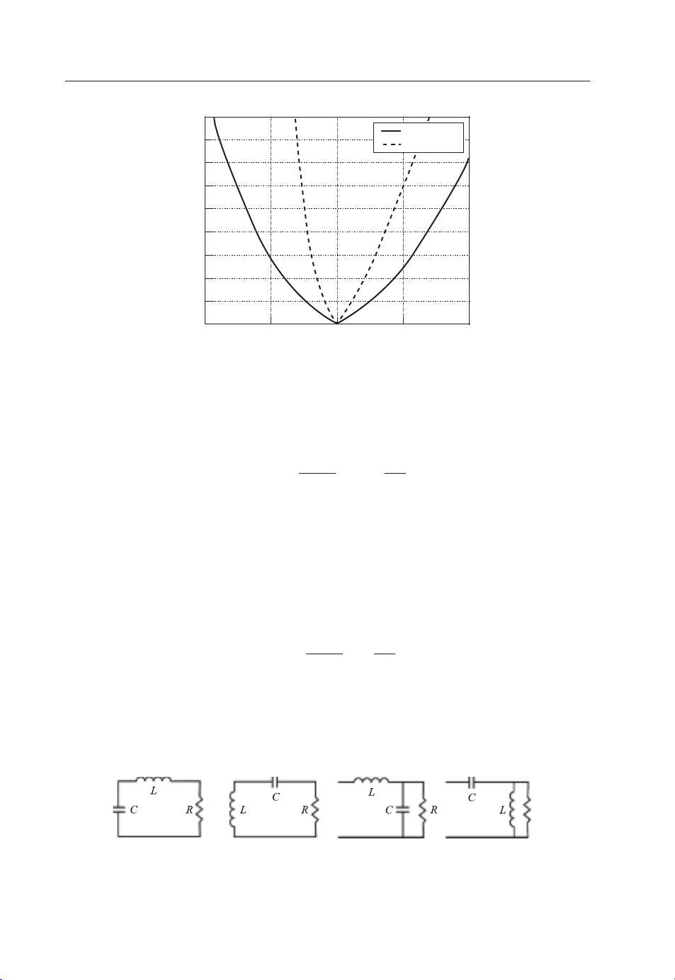
50 Antennas: From Theory to Practice
10
9
8
7
6
5
VSWR
4
3
2
1
900
Figure 2.19 VSWR of different designs as a function of frequency
950
Frequency in MHz
1000 1050
Design A
Design B
1100
circuits, a fundamental limitation for this, which can be expressed as [2]
∞
ln
0
1
|
(ω)
|
dω ≤
π
RC
(2.49)
This is known as the Bode–Fano limit for parallel RC. Since ln(1) = 0, there is no contribution
to this integral over frequencies for||= 1, so it can be seen that it is desirable to have
the maximum mismatch outside the band of interest if a broad bandwidth is required. If this
condition is assumed, the integral is limited to the bandwidth of interest (ω), and we can get
an idea of how well we can match an arbitrary complex impedance over that bandwidth. For
an idealized case, this equation can be simplified to
ω ln
|
(ω)
1
π
≤
|
RC
(2.50)
This clearly shows how the bandwidth (ω) is linked to the matching () and load impedance
(RC). For a given reflection coefficient (or VSWR) and the RC product, one can estimate the
maximum bandwidth attainable.
L
C
RR R
Figure 2.20 Four load impedances with LC matching networks
C
L
L
C
C
R
L
Page 67

Circuit Concepts and Transmission Lines 51
Similarly, the limits for the other three matching LC networks were obtained as:
Series RL: ω ln(
Series RC: ω ln(
Parallel RL: ω ln(
|
(ω)
|
(ω)
1
1
|
(ω)
) ≤
|
) ≤ πω
|
1
) ≤
|
π
R/L
πω
L/ R
0
2
RC
2
0
There are similar limitations on other forms of complex impedance. A general implication
of the Bode–Fano limit is that one should not waste any match out-of-band, and that the best
in-band match is obtained with Tchebyscheff rather than maximally flat networks. The best
broadband impedance-matching practice incorporates the complex load impedance into, for
example, a multisection filter structure with a design that includes the characteristics of the
load.
2.3.3 The Quality Factor and Bandwidth
The bandwidth is indeed a very important parameter for any electric/electronic component and
system. It is closely linked to the quality factor, Q, which is a measure of how much lossless
reactive energy is stored in a circuit compared to the average power dissipated.
Antenna bandwidth is maximized when the power dissipation is comparatively high. In
other words, a low Q is required for wide bandwidths. In turn, the extent to which this energy
is associated with radiation (rather than conductor or dielectric losses) determines the antenna
efficiency. For a circuit component such as an inductor or capacitor, we require the resistive
losses to be low; hence Q is required to be high. It is often the case that antennas and circuit
components have seemingly contradictory requirements: antennas are designed to have a low
Q, whereas circuit components are designed for a high Q.
The quality factor is quoted as being either unloaded or loaded. For the latter, the losses of
the external circuit – for example, the source – are included, whereas for the former they are
not. The unloaded quality factor, Q, is defined as
(
total energy stored
(
average power loss in the load
where W
field and P
Q ≡ ω
is the energy stored in the electric field, WMis the energy stored in the magnetic
E
is the average power delivered to the load. The loaded quality factor, QL, can also
L
be given by Equation (2.51) but with P
replaced by the total power PT, which is dissipated
L
)
)
= ω
W
E
+ W
P
L
M
in both the external circuit and the load.
At resonance, the electric and magnetic field energies have the same magnitudes and the
formulas simplify such that the unloaded quality factor at resonance Q
where ω
2ω
Q
is the angular resonant frequency (= 2π f0, where f0is the resonant frequency).
0
0WE
≡
0
P
2ω
0WM
=
L
P
L
is given by
0
(2.51)
(2.52)
Page 68

52 Antennas: From Theory to Practice
C
L
V
R
Figure 2.21 Series resonant circuit. (Reproduced by permission of Delft University Press)
There are many simplifications of these definitions that are widely used, but which only
truly apply when they are derived directly from the above. For example, a relation that is often
used is
where f
and f2are the frequencies at which the power reduces to half of its maximum value
1
at the resonant frequency, f
f
=
0
f2− f
Q
0
, and where BFis the fractional bandwidth. This relation only
0
1
=
B
1
F
(2.53)
truly applies to simple circuits, but is considered to be a good approximation to a wide range
of unloaded configurations. It has the advantage of providing a simple relationship between Q
and fractional bandwidth, but we will see later that it only accurately applies to simple, single
resonant circuits and should therefore be used with some care. The derivation of this relation
is illustrated below.
Consider the series resonant circuit shown in Figure 2.21. The power dissipated in the
resistance R is proportional to the square of the magnitude of the current I . This is plotted in
Figure 2.22 with R = 50 , L = 79.5775 nH and C = 0.3183 pF. The half-power frequencies,
4
3
2
冟I冟
(mA)
2
1
f
0.7 0.8 0.9 1 1.1 1.2 1.3
f
Frequency (GHz)
f2f
0
1
Figure 2.22 Relative power dissipated in a series resonant circuit around resonance
Page 69

Circuit Concepts and Transmission Lines 53
f1and f2, are found to be 0.9513 GHz and 1.0513 GHz respectively. As shown in Figure
2.22, the resonant frequency (when the current is maximized) is 1 GHz. Using Equation (2.53)
yields a Q
of 10.
0
It is possibleto find theunloaded quality factorof the circuitdirectly from thestored energies
of the inductor and capacitor. The magnetic and electric energies are given by
where V
1
W
=
M
is the voltage across the capacitor. Writing these and the power delivered to the load
C
2
, WE=
LI
2
1
2
CV
C
2
(2.54)
(i.e. the resistor, R) in terms of the current I gives
W
1
2
LI
2
, WE=
=
M
1
1
(
ω C
2
)
I2, PL= RI
C
2
2
(2.55)
Further substitution in Equation (2.51) yields
Q =
ω L +
2R
1
ω C
(2.56)
At resonance, the magnitudes of the electric and magnetic energies are equal and this relation
simplifies to
L
ω
Q
0
=
0
R
=
1
ω0CR
, and ω
1
=
√
0
LC
(2.57)
This formula is often used, but it should beunderstood that it only applies at resonance. Taking
R = 50 , L = 79.5775 nH and C = 0.3183 pF gives Q
= 10, as previously.
0
It is interesting to evaluate the ratio of Q at any frequency to that at resonance. From
Equations (2.56) and (2.57), this is given by
q =
Q
Q
1
ω
=
2
0
ω
0
ω
0
+
ω
(2.58)
It can be seen thatthe unloaded qualityfactor is aminimum at resonance,although the variation
with frequency is slow. For bandwidths of less than 20%, Q is approximately equal to Q
0
with
an error of less than 0.5% – i.e. the term in the parentheses of Equation (2.58) is approximately
equal to two over moderate bandwidths.
We wouldlike to derive a relationshipbetween the unloadedquality factor and thebandwidth
of the circuit. The bandwidth is normally taken to be the range of frequencies over which the
power dissipated; P
is greater than half of the maximum, PL0(at resonance). However, in the
L
sections that follow more general relations are derived based on a specified power transfer to
the load.
Page 70

54 Antennas: From Theory to Practice
The current in the circuit is given by
I =
R + jω L −
V
1
ω C
(2.59)
From Equation (2.59),the ratio ofthe power dissipatedat any frequency to the power dissipated
at resonance is given by
2
p =
P
P
I
L
L0
=
=
I
0
1 +
1
ω L
−
R
1
ω CR
2
(2.60)
This can be written
p =
1
1 +χ
2
(2.61)
where, from (2.57),
χ = Q
ω
0
ω
0
ω
0
−
ω
(2.62)
The relation given in Equation (2.61) can be solved to give
ω
Q
0
ω
ω
0
−
ω
0
=±
1 − p
p
(2.63)
This is a quadratic equation in ω with two positive and two negative solutions. The difference
between the two positive solutions is
1 − p
ω
ω
2
− ω1=
0
Q
p
0
(2.64)
This gives the fractional bandwidth as
f
− f
B
2
=
F
f
0
1
1
=
1 − p
Q
p
0
(2.65)
When p = 0.5, this simplifies to the familiar expression
1
B
=
F
Q
0
(2.66)
Page 71

Circuit Concepts and Transmission Lines 55
V
I
Figure 2.23 Parallel anti-resonant circuit. (Reproduced by permission of Delft University Press)
L
C
R
as previously seen in Equation (2.53). This derivation does not make any assumptions about
the numerical value of the quality factor or the bandwidth and is, therefore, applicable to both
high- and low-Q systems.
The response of a parallel resonant circuit – shown in Figure 2.23 – can be found in much
the same way as for series resonance.
The energies stored in the electric and magnetic fields of the capacitor and inductor respectively and the power dissipated in the resistance are given by
W
1
=
E
2
, WM=
CV
2
1
1
L
2
V2, P = GV
2
(
)
ω L
2
(2.67)
where G is the conductance. Substitution in Equation (2.51) gives
Q =
ω C +
2G
1
ω L
. (2.68)
At anti-resonance, the magnitudes of the electric and magnetic energies are equal and this
relation simplifies to
C
The ratio between Q and Q
ω
Q
is the same as for the series resonance, given by Equation (2.58).
0
0
=
0
G
=
1
ω0LG
(2.69)
It can also be shown (using the same method) that the fractional bandwidth is the same as for
the series resonant circuit.
The formulas for Q that have been derived so far have been for series and parallel resonant
circuits respectively. However, they are often applied – strictly incorrectly – to other circuit
combinations. We will see later that this can give large errors, so some care is required in
applying these formulas.
2.4 Various Transmission Lines
There are many transmission lines developed for various applications. The most popular ones
are shown in Figure 2.24. They are the two-wire transmission line, the coaxial cable, the
microstrip, the stripline, the coplanar waveguide (CPW) and the waveguide. We are going
to examine these transmission lines in terms of their characteristic impedance, basic mode,
frequency bandwidth, loss characteristic and costs.
Page 72

56 Antennas: From Theory to Practice
g
StriplineTwo-Wire
Coaxial Cable
Microstrip
Figure 2.24 Various transmission lines
Coplanar Waveguide (CPW)
Wave
uide
2.4.1 Two-wire Transmission Line
This is the simplest transmission line and its cross-sectional view is given in Figure 2.25. The
separation of the wires is D and the diameter of the wires is d. The medium between the wires
has a permittivity of ε.
It can be shown that the per unit length inductance and capacitance of the transmission line
are [2]:
μ
L =
ln
π
If the medium between the wires has a conductivity of σ
σ
, we can obtain the resistance and conductance of a unit length line as
2
R =
respectively.
D +
πd
2
√
D2− d
d
ωμ
2σ
2
, G =
2
, C =
D +
ln
πε
√
ln
, and the conductivity of the wire is
1
πσ
√
d
1
D2− d
D +
D2− d
2
2
(2.70)
(2.71)
d
D
ε
Figure 2.25 Two-wire transmission line
d
Page 73

Circuit Concepts and Transmission Lines 57
2.4.1.1 Characteristic Impedance
If the loss of the line can be considered very small, the characteristic impedance is given by
Equation (2.22), i.e.
Z
=
0
L
C
μ
=
π2ε
ln
√
120
D +
≈
√
ln
ε
r
D2− d
d
D +
√
D2− d
d
2
2
(2.72)
The typical value of industrial standard lines is 300 . This type of transmission line was
commonly used to connect a television receiving antenna (usually a folded dipole with an
impedance around 280 ) to a home television set many years ago. The uniform spacing is
assured by embedding the two wires in a low-loss dielectric, usually polyethylene. Since the
wires are embedded in the thin ribbon of polyethylene, the dielectric space is partly air and
partly polyethylene.
2.4.1.2 Fundamental Mode
The electromagnetic field distribution around the two-wire transmission line is illustrated
by Figure 1.15. Both the electric field and magnetic field are within the transverse (to the
propagation direction) plane, thus this mode is called the TEM (transverse electro magnetic)
mode. This means that it is nondispersive and the velocity is not changed with the frequency.
The plane wave can also be considered a TEM wave.
2.4.1.3 Loss
Since the lumped parameters of a transmission line are given by Equations (2.70) and (2.71),
the attenuation constant α can be calculated using Equation (2.14). However, the principal loss
of the two-wire transmission line is actually due to radiation, especially at higher frequencies.
Thus, this typeof transmission line isnot suitable forhigherfrequency applications. Thetypical
usable frequency is less than 300 MHz.
Some people may be familiar with the twisted-pair transmission line. As the name implies,
the line consists of two insulated wires twisted together to form a flexible line without the
use of spacers. It has relatively good EMC (electromagnetic compatibility) performance –
the twisted configuration cancels out the radiation from both wires and results in a small and
symmetrical total field around the line; but it is not suitable for high frequencies because of the
high dielectric losses that occur in the rubber insulation (low costs) as well as the radiation.
When the line is wet, the losses increase significantly.
2.4.2 Coaxial Cable
The coaxial cable consists of a central, insulated wire (inner conductor) mounted inside a
tubular outer conductor, as shown in Figure 2.26. In some applications, the inner conductor is
also tubular. The inner conductor is insulated from the outer conductor by insulating materials
Page 74

58 Antennas: From Theory to Practice
b
a
ε
Figure 2.26 The configuration of a coaxial line
Copper
core
Outer jacket
Insulating
material
Braided
outer
conductor
Protective
plastic
covering
which are made of Pyrex, polystyrene, polyethylene plastic or some other material that has
good insulating characteristics and low dielectric losses at high frequencies over a wide range
of temperatures. In order to ensure good EMC performance, shielded and double-shielded
coaxial cables have been developed and are available on the market. This type of transmission
line is widely used for RF engineering and antenna measurements and for the connection
between the antenna and transceiver.
Coaxial cablescome inthree basictypes: flexible, semi-rigid and rigid. The rigid cable gives
the best performance and is normally for high-performance and phase-sensitive applications,
whilst the flexible cables are cheap and, obviously, flexible. The semi-rigid cable is a compromise. As shown in Figure 2.26, the diameters of the inner and outer conductors of a cable are
denoted a and b respectively, and the relative permittivity of the insulating material is ε
dielectric material reduces the velocity of the wave inside the cable to c/
√
εr. Some common
. The
r
loading materials and corresponding velocities are shown in Table 2.2 [3].
If the conductivities of the insulating material are zero and it can be shown that the per unit
length parameters of the coaxial line are
μ
2π
b
ln
a
R =
b
G = 2πσ
a
L =
C = 2πεln
Table 2.2 Coaxial cable material and velocity
Dielectric type (ns/m) (% of c)
Solid polyethylene (PE) 5.05 65.9
Foam polyethylene (FE) 4.17 80.0
Foam polystyrene (FS) 3.67 91.0
Air space polyethylene (ASP) 3.77–3.97 84–88
Solid Teflon (ST) 4.79 69.4
Air space Teflon (AST) 3.71–3.94 85–90
f μ
πσ
2
1
Time delay velocity
1
1
+
(
)
a
b
b
ln
a
Propagation
(2.73)
Page 75

Circuit Concepts and Transmission Lines 59
E
H
Figure 2.27 Field distribution within a coaxial line
The velocity, as shown in Equation (2.25), is
v =
√
1
LC
1
=
√
εμ
c
=
√
ε
r
2.4.2.1 Characteristic Impedance
Normally, if the loss of the line can be considered very small, the characteristic impedance is
given by Equation (2.22), i.e.
Z
=
0
L
C
με
=
2π
b
60
ln
=
a
√
b
ln
ε
a
r
(2.74)
The typical value for industrial standard lines is 50 or 75 .
2.4.2.2 Fundamental Mode
The electromagnetic field distribution around the coaxial cable is illustrated by Figure 2.27.
Again, both the electric field and magnetic field are within the transverse (to the propagation
direction) plane, thus this field is TEM mode.
However, this is only true for the frequencies below the cut-off frequency, which is [2]
=
π(a +b)
v
(2.75)
f
c
where v is the velocity of the wave in the cable and the cut-off wavelength is
λ
= π(a + b) (2.76)
c
If theoperational frequency is above this cut-off frequency (or, say, the operational wavelength
is below the cut-off wavelength), the field within the coaxial cable may no longer be TEM
mode; some higher modes such as TE
(a transverse electric field, the magnetic field has
11
nontransverse component) mode may exist, which is not a desirable situation since the loss
could be significantly increased.
Page 76

60 Antennas: From Theory to Practice
2.4.2.3 Loss
Since the transmission line lumped parameters are given by Equation (2.73), the attenuation
constant α canbe calculated using Equation (2.14)or Equation(2.23) for a low-loss line;that is
√
0
2
f μεr(1/a + 1/b)
=
120√πσ2ln(b/a)
+
60πσ
√
ε
1
r
(2.77)
α ≈
2Z
R
GZ
+
0
which is a function of the coaxial dimensions a and b as well as the conductivity and
permittivity of the materials. When b/a ≈ 3.592 (which means that the typical characteristic
impedance should be around 77 ohms), the attenuation reaches the minimum. This is one of
the most important considerations when making the cable.
In addition to the characteristic impedance, mode and loss of a cable, there are some other
considerations when choosing a transmission line. Power-handling capacity is one of them,
since it is very important for radar and high-power applications. The breakdown electric field
strength in air is about 30 kV/cm (this means thebest characteristic impedance should be close
to 30 ohms). A list of some commercial cables with some important specifications is given in
Table 2.3, where OD stands for the outer diameter and Vmax is the maximum voltage which
may be applied to the cable in Volts. A more complete list can be found in [3]. It is clear that
there are over 100 industry standard cables on the market with various specifications. The one
with the smallest loss at 400 MHz is RG-211A, about 2.3 dB/100 ft. It is also one of the most
expensive cables – normally the cost is inversely proportional to the loss of the cable.
2.4.3 Microstrip Line
As shown in Figure 2.28, a microstrip line may be viewed as a derivative of a two-wire
transmission line and is perhaps the most widely used form of planar transmission line. One
side of the structure is freely accessiblefor themounting of packaged devices andthe geometry
lends itself extremely well to PCB patterning techniques to define the circuit. It has been used
extensively in microwave and millimeter circuits and systems.
Due to the complexity of the structure, the analytical expressions of per unit length parameters are difficult to obtain. The effective relative permittivity is approximated as
ε
≈
re
+
2
+ 1
ε
r
− 1
ε
r
2√1 +12d /W
(2.78)
This is an empiricalexpressionand is a functionofthe material property andtheratio W/d.W is
the widthof thestrip andd is the thickness of the substrate, which has a relative permittivity ε
2.4.3.1 Characteristic Impedance
The calculation of the characteristic impedance is not an easy task. From the transmission line
theory, the relation between the velocity and per unit length inductance and capacitance is
v =
√
1
LC
c
=
√
ε
re
.
r
Page 77

Circuit Concepts and Transmission Lines 61
Table 2.3 Some commercial coaxial cables and their specifications (Reproduced by permission of
RFCafe.com)
dB/100 ft
Dielectric Capacitance OD @400 Vmax
Type (/U) MIL-W-17 Z
RG-6A /2-RG6 75.0 PE 20.6 0.332 6.5 2700 Braid
RG-8 52.0 PE 29.6 0.405 6.0 4000 Braid
RG-8A 52.0 PE 29.6 0.405 6.0 5000 Braid
RG-9 51.0 PE 30.2 0.420 5.9 4000 Braid
RG-11A /6-RG11 75.0 PE 20.6 0.405 5.2 5000 Braid
RG-55B 53.5 PE 28.8 0.200 11.7 1900 Braid
RG-58A /28-RG58 52.0 PE 29.6 0.195 13.2 1900 Braid
RG-58C /28-RG58 50.0 PE 30.8 0.195 14.0 1900 Braid
RG-59/A /29-RG59 73.0 PE 21.1 0.242 10.5 2300 Braid
RG-59B /29-RG59 75.0 PE 20.6 0.242 9.0 2300 Braid
RG-141/A 50.0 ST 29.4 0.190 9.0 1900 Braid
RG-142/A/B /60-RG142 50.0 ST 29.4 0.195 9.0 1900 Braid
RG-164 /64-RG164 75.0 PE 20.6 0.870 2.8 10,000 Braid
RG-174 50.0 ST 0.100 17.3 1200 Braid
RG-177 /67-RG177 50.0 PE 30.8 0.895 2.8 11,000 Braid
RG-178/A/B /93-RG178 50.0 ST 29.4 0.072 29.0 1000 Braid
RG-180A/B /95-RG180 95.0 ST 15.4 0.140 17.0 1500 Braid
RG-188 50.0 ST 0.050 17.5 700 Braid
RG-211/A /72-RG211 50.0 ST 29.4 0.730 2.3 7000 Braid
RG-223 /84-RG223 50.0 PE 19.8 0.211 8.8 1900 Dbl Braid
RG-316 /113-RG316 50.0 ST 29.4 0.102 20.0 1200 Braid
RG-393 /127-RG393 50.0 ST 29.4 0.390 5.0 5000 Braid
RG-400 /128-RG400 50.0 ST 29.4 0.195 9.6 1900 Braid
RG-401 /129-RG401 50.0 ST 29.4 0.250 4.6 3000 Cu. S-R
RG-402 /130-RG402 50.0 ST 29.4 0.141 7.2 2500 Cu. S-R
RG-403 /131-RG403 50.0 ST 29.4 0.116 29.0 2500 Braid
RG-405 /133-RG405 50.0 ST 29.4 0.086 13.0 1500 Cu. S-R
() type (pF/ft) (in.) MHz (rms) Shield
0
Note: PE: Polyethylene; ST: Solid Teflon
Using Equation (2.18), the characteristic impedance can be expressed as
Z
L
=
0
=
C
vC
√
1
ε
re
=
cC
(2.79)
Thus, to compute the characteristic impedance, we just need to obtain the per unit length
capacitance C once the effective permittivity is known. This approach makes a difficult task
y
W
d
Figure 2.28 Microstrip line
r
x
Page 78

62 Antennas: From Theory to Practice
slightly easier. When the thickness of the metal strip can be neglected, it has been found that
[2]:
r
when W/d <1, the characteristic impedance of the line is
60
Z
=
√
0
It decreases monotonically to 126/
r
when W/d >1, the characteristic impedance of the line is
√
εras W/d increases to 1.
8d
ln
ε
W
r
W
+
4d
126
>
√
ε
r
(2.80)
Z
=
√
0
εr(W/d + 1.393 + 0.667 ln(W/d + 1.44))
120π
It also decreases monotonically from 126/
√
εras W/d increases. That is, the larger the ratio
126
<
√
ε
r
(2.81)
W/d, the smaller the characteristic impedance; also, the larger the permittivity, the smaller the
characteristic impedance. Practical limitations exist on the range of impedances that can be
manufactured. These limits depend on factors such as the dielectric constant, substrate height
and manufacturing capability. In general, the thinnest line that can be etched routinely with a
good photolithographicprocess is of the order of 0.1 mm. This then putsthe upperbound of the
impedance at90–120 .The lower bound isdetermined bythe linewidth, whichshould not be
comparable to a wavelength. The typical value of the characteristic impedance for industrial
standard lines is 50 or 75 .
2.4.3.2 Fundamental Mode
The electromagneticfield distributionaround themicrostrip line is illustrated by Figure (2.29).
Both the electric field and magnetic field are seen to be within the transverse plane. But half
of the wave is traveling in free space, which is faster than the other half wave traveling in the
substrate, thus this field is in what is called quasi-TEM mode, a sort of TEM mode.
A result of a microstrip line being an open structure is that circuits are subject to radiation.
This does not mean that they are dangerous to get close to, but the performance of a device or
circuit maybe affected. This is adirect consequenceof the ‘unterminated’ field lines illustrated
in Figure (2.29). Inreality, thefieldlines do notjusthang in free spacebutterminate on whatever
is close to the line. The exact relations concerning radiation from a microstrip are complicated
but, in general, narrow lines radiate less.
E
H
Figure 2.29 The field distribution of a microstrip
Page 79

Circuit Concepts and Transmission Lines 63
The first higher mode in a microstrip line is the transverse electric TE10mode, its cut-off
wavelength is twice the strip width. After taking the material and fringing effects into account,
the cut-off frequency can be expressed approximately as
λ
≈√εr(2W + 0.8d) (2.82)
c
However, the mode analysis of a microstrip is actually more complicated than this. In addition
to the conventional higher order modes, surface modes may exist. The surface mode does not
need the metal strip; it only needs the ground plane and the substrate. The lowest transverse
electric mode is TE
and its cut-off frequency is
1
√
2
( f
c)TE
=
1
8d√εr− 1
3c
(2.83)
The lowest transverse magnetic mode is TM
and its cut-off frequency is
0
√
2
c
=
4d√εr− 1
, thus, in order to keep the quasi-TEM mode
0
(2.84)
Obviously ( f
c)TE
= 1.5 · ( fc)
1
TM
( f
> ( fc)
0
c)TM
0
TM
propagation, the operational frequency of a microstrip line should be smaller than the cut-off
frequency of the TE
mode in Equation (2.82) and the cut-off frequency of the TM0mode in
10
Equation (2.84). Higher order modes will cause significant power loss via conductive loss and
radiation loss. The surface mode may transmit the power to any direction, which is, of course,
not desirable.
2.4.3.3 Loss
The loss of a microstrip line comes from the conductor loss and dielectric substrate loss.
The radiation loss is negligible at low frequencies. For most microstrip lines, conductor loss
is much more significant than dielectric loss. The attenuation constant can be calculated
approximately by
R
s
=
Z0W
(2.85)
where R
α
c
=ωμ2σ is the surface resistivity of the conductor.
s
A summary of some of the common substrates is given in Table 2.4. The first five are hard
substrates and the rest are considered soft substrates.
2.4.4 Stripline
A stripline is a conductor sandwiched by a dielectric between a pair of ground planes. It may
be viewed as an evolved structure from a coaxial cable, as shown in Figure 2.30. In practice,
a stripline is usually made by etching circuitry on a substrate that has a ground plane on
Page 80

64 Antennas: From Theory to Practice
Table 2.4 Some common substrates for a microstrip at 10 GHz
Substrate ε
r
Loss tangent Comments
Alumina (Al2O3) 9.8 0.0004 Low loss and cost, stable, difficult to machine
but very hard-wearing
LaAlO
3
24 0.0001 Low loss, but very expensive
MgO 9.8 0.00001 Very low loss but expensive and fragile
Quartz (SiO
) 3.8 0.0004 Low loss and low permittivity, good for mm
2
range, fragile
Sapphire (Al
) 9.4 and 10.8 0.00002 Very low loss, single crystal and anisotropic
2O3
material, expensive
Epoxy (FR4) 4.43@ 1 GHz 0.01 Relatively high lossand low cost, popular PCB,
up to ∼ 2 GHz
FR2 (flame resistant 2) 4.5@ 1 MHz 0.025 Similar to FR4, cheap, but recommend above
∼ 1 GHz
GaAs 13.0 0.0006 Low loss, not cheap, widely used for MMICs
LCP 3.1 0.002 Medium loss, low permittivity, up to 40 GHz,
cheap
PTFE (Teflon) 2.1 0.0004 Low loss, medium cost, low permittivity
PTFE-glass 2.1–2.55 ∼ 0.001 Medium loss and cost, low permittivity
PTFE-ceramic 10.2 0.002 Medium loss, high permittivity soft substrate,
not cheap
RT/Duroid 5870 2.33 0.0012 Medium loss, low cost and low permittivity, up
to 40 GHz
RT/Duroid 5880 2.22 0.0009 Low loss, low cost and low permittivity, up to
77 GHz
RT/Duroid 6002, 6202 2.94 0.0012 Medium loss, low cost and low permittivity
RT/Duroid 6006, 6.15 0.0019 Mediumloss, lowcost and medium permittivity
RT/Duroid 6010 10.2 0.0023 Medium loss, low cost andmediumpermittivity
the opposite face, then adding a second substrate (which is metalized on only one surface)
on top to achieve the second ground plane. The stripline is often considered a ‘soft-board’
technology, but using low-temperature co-fired ceramics (LTCC), ceramic stripline circuits
are also possible.
Unlikea microstrip line, the stripline isbasicallyanenclosedstructure;thefield is not affected
by nearby components. The effective permittivity is the same as the substrate permittivity.
d
Figure 2.30 From a coaxial cable to a stripline
W
t
Page 81

Circuit Concepts and Transmission Lines 65
There are many advantages of using striplines. Whatever circuits are on a microstrip (which
is a quasi-TEM mode structure), you can do better by using a stripline, unless you run into
fabrication or size constraints. Stripline filters and couplers always offer better bandwidth than
their counterparts in a microstrip. Another advantage of the stripline is that fantastic isolation
between adjacenttraces can be achieved (unlike a microstrip). Thebest isolationresults when a
picket-fence of vias surrounds eachtransmission line,spaced at less than aquarter-wavelength.
The stripline can be used to route RF signals across each other quite easily when an offset
stripline (i.e. the central conductor is not right at the middle between the two ground planes)
is used.
There are two major disadvantages of a stripline:
1. It is much harder and more expensive to fabricate than the microstrip. Lumped-element and
active components either have to be buried between the ground planes (not as convenient
as a microstrip), or transitions to the microstrip must be employed as necessary to get the
components onto the top of the board.
2. Because of the second ground plane, the strip width is much narrower for given impedance
(such as 50 ohms) and the board is thicker than that for a microstrip. A common reaction to
problems with microstrip circuits is to convert them to a stripline; this may result in a much
larger thickness for the same loss of the transmission line.
2.4.4.1 Characteristic Impedance
The characteristic impedance can be calculated approximately by
30π
√
W
ε
r
d − t
Z
=
0
+ A
(2.86)
where
A =2B ln(B + 1) − (B − 1) ln(B
√
B = 1
1 −t /d
2
− 1)/π
The impedance is sensitive to the thickness of the central conductor. The typical value for
industrial standard lines is 50 or 75 .
2.4.4.2 Fundamental Mode
Just as for the field within a coaxial cable, the field in a stripline is TEM mode. This means
that it is nondispersive and the velocity is not changed with frequency.
It is also possible to generate higher order modes if the operational frequency is above the
lowest cut-off frequency. The smallestwavelengthshould meet thefollowingcondition to avoid
higher order modes:
λ
> 2d√ε
min
λ
min
> 2W√ε
r
r
(2.87)
Page 82
66 Antennas: From Theory to Practice
W
G
t
d
Figure 2.31 Evolution from a coaxial cable to CPW (G: gap: W: width; d: substrate height)
G
r
2.4.4.3 Loss
The loss characteristics of the stripline are similar to the microstrip but have little loss due to
radiation, as the structure is almost screened.
2.4.5 Coplanar Waveguide (CPW)
The CPWis anotherpopular planar transmission line. Just like a stripline, it may be considered
a structure evolved from a coaxial cable, as shown in Figure 2.31. This structure can also be
viewed as a coplanarstripline. The central conductor is separated from a pair of ground planes.
They all sit on a substrate with a dielectric permittivity of ε. In the ideal case, the thickness
of the dielectric is infinite; in practice, it is just thick enough so that EM fields die out before
they get out of the substrate. A variant of the coplanar waveguide is formed when a ground
plane is provided on the opposite side of the dielectric; this is called a grounded coplanar
waveguide (GCPW) and was originally developed to counter the power dissipation problems
of CPW.
The CPW offers many advantages, which include the following:
r
It iseasy tofabricate and to integrate into circuits. Circuit components can be easily mounted
on top of the line (even easier than on a microstrip) due to the fact that both the conductor
and ground plane are on the same side of the substrate. Unlike the microstrip and stripline,
no vias are required.
r
It can work to extremely high frequencies (100 GHz or more). Connecting to a CPW does
not entail any parasitic discontinuities in the ground plane.
r
Good circuit isolation can be achieved using a CPW, because there are always RF grounds
between traces. Many examples of high-isolation RF switches have used a grounded CPW
to get 60 dB isolation or more.
r
The characteristic impedance can be kept as a constant as the signal conductor’s width is
tapered down/up tomeet apin. This is perfect formatching to a component pin width without
changing the substrate thickness.
One disadvantage is potentially lousy heat dissipation - this depends on the thickness of the
line and whether it makes contact with a heat sink. In addition, in terms of the circuit size, the
CPW isat a disadvantage versus a stripline or microstrip circuit; becauseits effective dielectric
constant is lower (half of the fields are in air). CPW circuits can be lossier than comparable
microstrip circuits if a compact layout is required.
Page 83

Circuit Concepts and Transmission Lines 67
2.4.5.1 Characteristic Impedance
The design formulas for aCPW are verycomplicated. There are four geometricparameters: the
gap G, the conductor width W and thicknesst and thesubstrate thicknessd.It is not possible to
obtain an accurate analytical expressionof the characteristic impedance. Some approximations
have to be made. If the conductor thickness is neglected, the effective permittivity is given
approximately by [2]
+ 1
ε
ε
r
=
re
+
tanh[0.775 ln(d/G) +1.75]
2
kG
[0.04 −0.7k + 0.01(1 − 0.1ε
d
)(0.25 +k)]
r
(2.88)
where
k =
W
W + 2G
(2.89)
The effective dielectric constant of a CPW is very close to the average dielectric constant of
the substrate and free space. One way to think about this is that half of the electric field lines
are in free space and half are in the dielectric.
The characteristic impedance is
Z
=
√
0
ε
K(k)
re
(2.90)
K(k)
30π
where K (k) is a complete elliptical function of the first kind. We have
k
=√1 −k2; K(k) = K (k)
(2.91)
and
K
(k)
K(k)
1
=
1 +
ln(2
π
1 −√k
1
1 +
ln(2
π
1 −√k
√
√
k
)
k
)
if 0 < k < 0.707
−1
if 0.707 < k < 1 (2.92)
Again, the typical impedance value for industrial standard lines is 50 or 75 .
Page 84

68 Antennas: From Theory to Practice
2.4.5.2 Fundamental Mode
The EMfield distribution around the CPW is illustrated in Figure2.31 andis similarto that of a
microstrip. The wave velocity in the air isfaster than that in the substrate, thus the fundamental
field of CPW is quasi-TEM mode.
Higher order modes and surface modes may be generated in a CPW just as in a microstrip
line. Thus, ground straps (bounding wires) are normally needed to tie the two grounds together
in a CPW. These are especially important around any discontinuity, such as a tee junction.
Care has to be taken since the bounding wires themselves could be the cause of discontinuity!
2.4.5.3 Loss
The current on the CPWis concentrated aroundthe signal conductor. The current onthe ground
planes is also very focused in a small area, which results in a relatively high conductor loss as
well as a heat dissipation problem. Generally speaking, the CPW exhibits a higher loss than
its microstrip counterpart.
2.4.6 Waveguide
This is a very special and unique electromagnetic transmission line. Unlike any other transmission lines, a waveguide consists of just one piece of metal, which is tubular, usually with
a circular or rectangular cross-section. A rectangular waveguide is shown in Figure 2.32. Due
to the boundary conditions that the electric and magnetic fields have to satisfy, there are many
possible wave patterns, which are called transverse electric (m, n) modes (TE
transverse magnetic (m, n) modes (TM
the x and y axes respectively. For example, TE
modes). m and n represent thenumber of peaksalong
mn
mode means that the electric field is within
10
the transverse plane and there is no electric field component along the propagation direction,
whilst the magnetic field is not confined to the transverse plane, and the electric field changes
along the x -axis, having one peak, but it has no changes along the y-axis. Which modes will
actually be generated inside a waveguide depend on the frequency and excitation.
If the frequency is below the cut-off frequency of the fundamental mode (which is TE
mode for standard waveguides), no propagation mode can be generated. Thus, the operational
frequency should be greaterthan thecut-off frequency, which means that the waveguide can be
modes) and
mn
10
y
b
E
Figure 2.32 Rectangular waveguide
TE
mode
10
a
x
Page 85

Circuit Concepts and Transmission Lines 69
considered ahigh-pass filter. Anysignals below the cut-off frequency will be filtered out by the
waveguide. The larger the waveguide, the lower the cut-off frequency. Since large waveguides
are heavy and expensive, they are not attractive for applications. Thus, waveguides are only
used for microwave and millimeter wave frequency bands.
The main advantages of the waveguide are low loss and high power-handling capacities,
which are very important for high-power applications such as radar.
2.4.6.1 Fundamental Mode
The fundamental mode of a standard rectangular waveguide is TE
mode. The field pattern
10
(along with some higher modes) is illustrated in Figure 2.32 (the field patterns for some higher
modes can be found in [2] and [4]). The width and height of the waveguide are a and b
respectively. The electric field can be expressed as
π
E
= E0sin(
y
Ex= Ez= 0
j(ωt−βz)
x)e
a
(2.93)
and the magnetic field is given by
π
H
= H1sin(
x
Hy= 0
H
= H2cos(
z
j(ωt−βz)
x)e
a
π
j(ωt−βz)
x)e
a
(2.94)
The electric field is indeed within the transverse plane and the maximum field is at x = a/2,
while the magnetic field has two components, one along the propagation direction z. Neither
the electric nor the magnetic field is a function of y, i.e. the mode index n = 0.
2.4.6.2 Cut-off Frequency, Waveguide Wavelength and Characteristic Impedance
The cut-off wavelength for TE
and TMmnmodes is given by
mn
2
m
(
a
n
2
)
+ (
b
λ
=
c
(2.95)
2
)
and its corresponding cut-off frequency is
1
Thus, for TE
f
=
c
2√εμ
mode, the cut-off wavelength is λc= 2a. This means that the waveguide works
10
m
(
a
n
2
)
+ (
2
)
b
(2.96)
for the operational wavelength λ<2a.
Since the next highest mode to TE
a higher mode than TE
) and its cut-off wavelength is λc= a, this waveguide is only suitable
20
is TE20(for a standard waveguide, 2b < a, i.e. TE01is
10
for the operational wavelength between these two cut-off wavelengths,i.e. a <λ<2a. Outside
Page 86

70 Antennas: From Theory to Practice
Table 2.5 Standard waveguides
Waveguide Freq. (GHz) ID of a (mm) ID of b (mm) Freq. band
WR-137 5.85–8.2 34.85 15.80 C band
WR-112 7.05–10.00 28.50 12.60 H band
WR-90 8.2–12.4 22.86 10.16 X band
WR-62 12.4–18.0 15.80 7.90 Ku band
WR-51 15.0–22.0 12.96 6.48 K band
WR-42 18.0–26.5 10.67 4.32 K band
the bounds, the frequency is either too low for transmission or too high to keep single-mode
transmission. Higher modes are not desirable since they have higher loss and the field pattern
may be changed over the transmission. Thus, eachindustrialstandardwaveguide isonlysuitable
for a certain frequency range. A list of some selected standard waveguides with their suitable
frequency ranges and inside dimensions is given in Table 2.5.
The field inside a waveguide exhibits a periodic feature and the period is one waveguide
wavelength, which is actually different from (longer than) the free space wavelength. The
waveguide wavelength can be calculated using
λ
= λ
g
1 −(
λ
2
)
λ
c
(2.97)
It is determined by the free space wavelength λ and the cut-off frequency λ
The characteristic impedance is also mode-dependent. For TE
Z
TE10
= 120π
1 −(
λ
2a
mode, it is
10
) (2.98)
.
c
which is not a constant but a function of frequency. This is one of the reasons why the single
mode is preferred for waveguide applications.
In this sectionsix of themost popular transmissionlines have been introducedand discussed.
The characteristic impedance, fundamental mode and loss characteristics have been presented.
A brief summary is provided in Table 2.6.
2.5 Connectors
In practice, almost all transmission lines have to be terminated to suitable connectors, which
make the device interconnection much easier. There are many types of industrial standard
connectors. Sometimes, more than one connector is available. For example, RG58 cable can
be assembled to SMA, SMB, BNC and Type N connectors. Making the right choice can be a
problem and there is a lack of information on this practical subject in other books, hence we
will address this issue in this section.
Connectors are developed as a pair: a male and a female (an example is shown in
Figure 2.33), although some RF connectors are sexless (such as the APC-7 and the
Page 87

Circuit Concepts and Transmission Lines 71
Table 2.6 Summary of various transmission lines
Two-wire Coax Microstrip Stripline CPW Wave-guide
Basic mode TEM TEM quasi-TEM TEM quasi-TEM TE
Bandwidth narrow – low
freq
Loss high med. med. med. med. low
Cost low low/ med. med. med. med. high
Ease of
integration
Application low freq.,
med. hard easy med. easy hard
short
distance
wide wide wide very wide narrow
general
purpose
PCB circuit
and MMIC
RF circuit
and MMIC
RF circuit
and MMIC
10
high power
and high
freq.
General Radio GR874). It is very important to choose the right connector for the application, since the effects of the connector (which is an additional element and may not have been
taken into account in the design) on the system performance and measurements may be quite
significant. This is especially true in antenna measurements.
A good summary of all RF/microwave connectors was given by Amphenol RF [5]. Table
2.7 is a selection of some popular connectors for antenna systems and measurements. These
connectors are mainly for coaxial cables, but some of them can be used for other transmission
lines. For example, theSMA straight PCBmount jack, tabterminal panel jack andstub terminal
panel jack are available and widely used in the antenna community.
Since all RF test equipment comes with coaxial connectors (type N and SMA are popular
connectors), direct connection with other forms of transmission lines (such as microstrip and
CPW) would be tricky. Some adapters have been developed. For example, industrial standard
coax-to-waveguide adaptors are now widely available on the market. Figure 2.34 shows how
to connect an SMA connector directly to a microstrip and CPW (feed line to an antenna) in
practice – no standard adaptor is available.
Figure 2.33 Male (left) and female (right) N-type connectors
Page 88

72 Antennas: From Theory to Practice
Table 2.7 Some industry standard connectors (Reproduced by permission of Amphenol RF)
BNC Baby N connector (BNC). Bayonet-style coupling for quick connection and
disconnection. Available in 50 ,75 and 50 reverse polarity. DC–4GHz
K The K ConnectorTMis a precision coaxial connector system that operates up to 40
GHz. It is compatible with SMA, WSMA and 3.5 mm connectors. It is well suited
to applications in components, systems or instrumentation.
MCX A snap-on miniature coaxial (MCX) connector that conforms to the European
CECC 22220.Since the MCX has identicalinner contactand insulator dimensionsto
the SMB while being 30% smaller, it provides designers with options where weight
and physical space are limited. DC – 6 GHz.
MMCX A micro-miniature coaxial (MMCX) connector with a lock-snap mechanism allowing for 360 degrees rotation on a printed circuit board. Conforms to the
European CECC 22000 specification and comes in surface mount, edge card and
cable connectors. DC – 6 GHz.
Precision:APC-2.4, APC-3.5, APC-7 and APC-N TheacronymAPCdescribeshighperformance precision connectors, and stands for Amphenol Precision Connectors.
Developed by Amphenol and Hewlett-Packard engineers. DC – 50 GHz.
Mini BNC A new generation of miniature BNC connectors that maintain the
positive characteristics of our full-size BNCs for 75 systems while allowing 40%
more interconnects in the same area. DC – 11 GHz.
SMA Subminiature version A (SMA) connectors with a threaded coupling mechanism that perform through 18 GHz. Available in standard, phase adjustable and reverse polarity. Built in accordance with MIL-C-39012 and CECC 22110/111, SMA
connectors can bemated with allconnectors that meetthese specs, regardless ofmanufacturer. Widely used with RG-55, 58, 141, 142, 223, 303, 122, 174, 188 and 316.
SMB Subminiature version B(SMB) connectors. Developedin the 1960s asasmaller
alternative to the SMA, the SMB line features a snap-on coupling mechanism. Available in 50 ,75 and miniature 75 . DC – 4 GHz (usable to 10 GHz). Often used
with RG-188 and 196.
(continued)
Page 89

Circuit Concepts and Transmission Lines 73
Table 2.7 Some industry standard connectors (Reproduced by permission of Amphenol RF)
(Continued)
SMC Subminiature version C(SMC) connectors. Medium-sized 50 threaded con-
nectors designed to meet MIL-C-39012 category D, as generated by the US Air
Force. DC – 4 GHz (usable to 10 GHz). Often used with RG-188 and 196.
SMP Subminiature connectors with a frequency range up to 40 GHz. Used in miniaturized applications they feature both push-on and snap-on mating styles.
SSMB Scaled SMA (SSMA). Microminiature connectors with snap-on mating interface allowing quick installation in small spaces with excellent performance in
devices up to 4 GHz.
TNC Features screw threads for mating and serves as a threaded version of the BNC
connector. The TNC is a 50 connector available in both standard and reverse
polarity. DC – 11 GHz.
Type NAvailable in standardN (coaxial cable) andcorrugated N (helical andannular
cable), the Type N is a durable, weatherproof, medium-sized connector consistent
through 11 GHz. Used with RG-8, 58, 141 and 225.
UHF Invented for use in the radio industry, UHF stands for ultra-high frequency.
While at the time 300 MHz was considered high frequency, these are now general
purpose connectors for low-frequency systems.
Figure 2.34 Wideband antennas fed by CPW and microstrip, which are directly connected/soldered to
SMA connectors
Page 90

74 Antennas: From Theory to Practice
2.6 Summary
This chapterhas provided comprehensive coverage of circuit concepts and transmission lines–
this is essential knowledge for antenna feeding, matching and characterization. In summary:
r
An introduction to lumped element systems and distributed element systems has been given
right at the beginning. The main idea is that the current, voltage and impedance are all
functions of the frequency and the reference position at the transmission line.
r
A transmission line model has been developed to obtain the important parameters of a
transmission line, which include the characteristic impedance, input impedance, attenuation
constant, phase constant and velocity. An extensive study on terminated transmission lines
has been carried out. The reflection coefficient, return loss and VSWR have been introduced
to evaluate the line impedance matching.
r
The Smith Chart has been introduced as a very useful tool to analyze impedance matching.
Lumped and distributed matching networks and impedance-matching techniques have also
been addressed.
r
The bandwidth and quality factor (Q factor) have been discussed in depth.
r
Six popular transmission lines have been examined and compared in terms of
their characteristic impedance, fundamental mode, loss characteristics and frequency
bandwidth.
r
Various RF/microwave cables and connectors have been presented at the end of this chapter
along with their typical specifications and frequency bandwidths.
References
[1] J. D. Kraus and D. A. Fleisch, Electromagnetics with Applications, 5th edition, McGraw-Hill, Inc., 1999.
[2] D. M. Pozar, Microwave Engineering, 2nd edition, John Wiley & Sons, Inc., 1997.
[3] http://www.rfcafe.com/references/electrical/coax
[4] C. S. Lee, S. W. Lee and L. L. Chuang, ‘Plot of modal field distribution in rectangular and circular waveguides’,
IEEE Trans. on MTT, March, pp. 271–274, 1985.
[5] www.amphenolrf.com
chart.htm
Problems
Q2.1 Explain the concept of the characteristic impedance of a transmission line.
Q2.2 For a low-loss transmission line, find its characteristic impedance, attenuation con-
stant and phase constant (or wave number using lumped elements). How does the
frequency affect these parameters?
Q2.3 A uniform transmission line has constants R =500μ/m, G = 1.5mS/m, L =
0.5μH/m and C = 10nF/m. Find the characteristic impedance and the attenuation constant of the line at the following frequencies
a) 50 Hz;
b) 30 MHz;
c) 1 GHz;
d) 10 GHz.
and comment on the results.
Page 91

Circuit Concepts and Transmission Lines 75
Q2.4 A coaxial transmission line has a = 4 mm and b = 12 mm. Find the characteristic
impedance of the line if the dielectric is
a) air space polyethylene (ASP);
b) foam polyethylene (FE);
c) solid Teflon (ST).
Hint: Use Table 2.2 for permittivity.
Q2.5 A 100 resistor is connected to a good cable with characteristic impedance of
50 . The attenuation constant is not zero but 0.2 Np/m at 1 GHz, and the relative
permittivity of the cable dielectric is 1.5. If the cable length is 10 m, find
a) the reflection coefficient and return loss at the termination;
b) the reflection coefficient and return loss at the input of the cable;
c) the VSWR at both the terminal and the input of the cable;
d) the input impedance at the input of the cable.
Suggest a method to improve the matching of the system.
Q2.6 Obtain the theoretical characteristic impedance and the best impedance for maxi-
mum power-handling capacity of a coaxial cable. Use the results to justify why the
most common coaxial cable impedances are 50 and 75 .
Q2.7 RG-59U, a popular cable for microwave applications, has an open-circuit
impedance of 130 + j 75 ohmsand short-circuitimpedance of30.3 − j 21.2ohms.
Find the characteristic impedance of the line.
Q2.8 A quality transmission line is terminated in 100 + j 50 ohms. Find
a) the voltage reflection coefficient;
b) the VSWR;
c) the shortest length of line required to transform the impedance to purely resis-
tive.
If 220 V is applied to the line, find the maximum and minimum line voltages.
Q2.9 Explain the concept of impedance matchingand then comparea lumped matching
network and a distributed matching network.
Q2.10 Explain what the Smith Chart is. Explain its application.
Q2.11 A load with an impedance of 100 − j 100 is to be matched with a 50 trans-
mission line. Design a matching network and discuss if there are other solutions
available.
Q2.12 A load with animpedance of 100 − j 100 is to be matchedwith a 50 transmis-
sion line. Design two stub-matching networks and then compare their bandwidth
performance.
Q2.13 Explain what Bode–Fano limits are and how they may be applied to matching
networks.
Q2.14 Discuss the relationship between bandwidth and quality factor. What is the major
difference between the loaded Q factor and the unloaded Q factor?
Q2.15 Design a 50-ohm microstrip line using a PCB board with PTFE (Teflon) substrate
of 1 mm thickness. Find the cut-off frequency for the first higher mode in the line.
Q2.16 Design a 50-ohm CPW using a PCB board with PTFE (Teflon) substrate of 1 mm
thickness.
Q2.17 Rectangular waveguides are widely used for radar applications. WR-90 standard
waveguide (see Table 2.5) is mainly used for the X band. Find
a) the cut-off frequency for TE
b) the cut-off frequency for TE
c) the cut-off frequency for TE
10
01
20
mode;
mode;
mode.
Hence identify the most suitable frequency range for this waveguide.
Page 92

Page 93

3
Field Concepts and Radio Waves
In this chapter we will first see how Maxwell’s equations can be used to obtain wave solutions.
The concepts of the plane wave, intrinsic impedance and polarization will then be introduced,
followed by a discussion on radio propagation mechanisms and radio wave propagation characteristics in various media. A few basic radio propagation models will be introduced, and
circuit concepts and field concepts will be compared at the end of this chapter. The concept of
skin depth will be lookedinto from both the fieldand circuitpoints of view. Althoughthe issues
addressed in this chapter may not be used directly for antenna design, the knowledge will be
extremely useful for gaining a better understanding of the antenna radiation characteristics as
well asradio waves – generated/received by antennas. Because antennas and radio propagation
are so closely linked, some countries and universities treat them as a single subject.
3.1 Wave Equation and Solutions
As mentioned in Chapter 1, Maxwell’s modified version of Ampere’s Circuital Law enables
a set of equations to be combined together to derive the electromagnetic wave equation. The
derivation is relatively straightforward.
Now let us discuss a time-harmonic case with the time factor e
frequency and is the most common form of a wave in real life (according to Fourier’s theory,
more complicated cases may be decomposed to a linear combination of harmonic waves).
From Maxwell’s equations (1.29), we have
jωt
, which means a single
∇×E =−jωμH
∇×H = (σ + jωε)E
∇•E = ρ/ε
∇•H = 0
Take a curl operation on the first equation to yield
∇×∇×E =∇(∇•E) −∇
Antennas: From Theory to Practice Yi Huang and Kevin Boyle
C
2008 John Wiley & Sons, Ltd
2
E =−jωμ∇×H
(3.1)
Page 94

78 Antennas: From Theory to Practice
2
2
2
∂
+
∂z
.
2
2
where ∇2=∇•∇=
∂x
∂
∂
+
2
∂y
Combine this with the second and third equations in Equation (3.1) to obtain
2
∇
E − jωμ(σ + j ωε)E =∇(ρ/ε) (3.2)
Now let
γ =
jωμ(σ + jωε) = α + jβ (3.3)
where α and β are theattenuation constant andphaseconstant, respectively. Similardefinitions
were introduced for a transmission line in Chapter 2. From Equation (3.3) we can represent
these constants by the material properties and frequency as:
√
α = ω
με
β = ω√με
1
2
1
2
1 +
1 +
σ
ε2ω
σ
ε2ω
− 1
+ 1
1/2
1/2
(3.4)
2
2
2
2
Equation (3.2) can now be rewritten as
2
∇
E − γ2E =∇(ρ/ε) (3.5)
In the source-free region (ρ = 0), we have
2
∇
E − γ2E = 0 (3.6)
This is called the wave equation. There are many possible solutions to this equation. Boundary
conditions and sources are required to obtain the specific solutions. In free space, one of the
solutions is
E = ˆxE
e
0
jωt−γ z
= ˆxE0e
−αz+j (ωt−β z)
(3.7)
This can be validated easily by using this representation in the wave equation. Other possible
solutions include, for example
E = ˆxE
e
0
jωt+γ z
; E = ˆyE0e
jωt+γ z
; E = ˆz E0e
jωt±γ x
; ...
Using the electric field E in Equation (3.7) and Equation (3.1), the magnetic field H is
H =
j
∇×E =−ˆy
ωμ
jγ
ωμ
−αz+j (ωt−β z)
e
E
0
(3.8)
Page 95
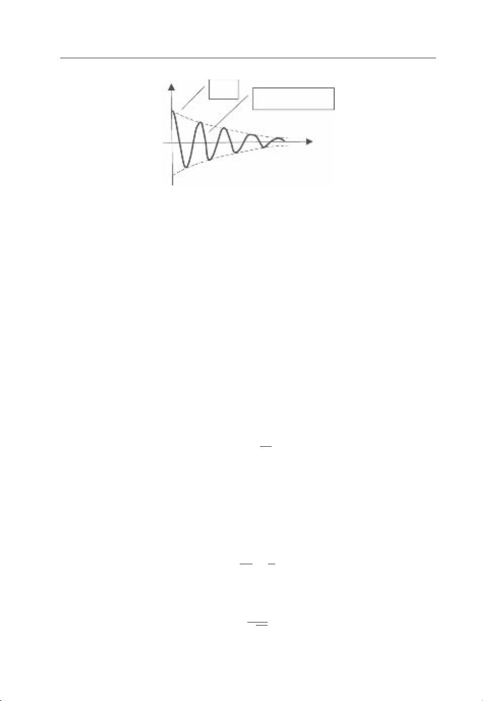
Field Concepts and Radio Waves 79
E
−αz
e
Figure 3.1 A traveling wave in a medium with loss
E0e
−αz
cos(ωt – βz)
z
Thus, themagnetic field has only a y component in thiscase, whichis orthogonal to the electric
field. There is a phase difference between the electric and magnetic fields if the attenuation
constant is not zero.
3.1.1 Discussion on Wave Solutions
Equation (3.7) can be illustrated by Figure 3.1; it is evident that
r
The wave solution is a vector. In this case, it has only an x component.
r
Its amplitude is decreased exponentially as a function of the propagation distance (z, in this
case). The attenuation constant α, given by Equation (3.4), is determined by the material
properties and frequency. When the conductivity σ is zero, the wave amplitude is a constant.
r
Its phase ϕ is of the form (ωt − βz), which is a function of time, frequency and propagation
distance.
For the loss-free case, σ = 0, Equation (3.4) can be simplified to
α = 0
β = ω
√
με
(3.9)
If we fix the phase and let the wave travel a distance of z over a period of time t,
mathematically this is
ϕ = ω · t + β ·z = 0 (3.10)
Thus, the velocity of the wave can be obtained as
z
t
ω
=
β
(3.11)
v =
Replace β by Equation (3.9) to give
1
v =
√
με
(3.12)
Page 96

80 Antennas: From Theory to Practice
This means that the wave velocity is determined by the permittivity and permeability of the
medium in which the wave is traveling. In free space this velocity is
√
1
≈ 3 × 10⁸m/s
μ0ε
0
v =
We can therefore conclude that the velocity of an electromagnetic wave (including light) in
free space is about 3 × 10
8
m/s – this was what Maxwell obtained more than 120 years ago
when he formulated the four equations (more precisely 20 equations in his original work),
but at that time nobody could validate this important result. This is a good example of how
mathematics can be used to solve real world engineering problems.
In addition, from Equation (3.11), we can see that
ω
β =
2π f
=
v
2π
=
v
λ
(3.13)
Thus, the phase constant is also called the wave number (for every one wavelength, the phase
is changed by 2π ), which is the same as what we obtained for a transmission line in Chapter
2. In fact, the transmission line equation (2.7) is just a special case of the wave equation (3.6)
when x and y are fixed. The free space could be viewed as an open transmission line where
the information is carried by electromagnetic (EM) waves.
Light, X-rays and radio waves are EM waves at different frequencies although they seem
to be very different. One thing that all the forms of EM waves have in common is that they
can travel through empty space. This is not true for other kinds of waves; sound waves, for
example, need some kind of material, like air or water, in which to move. EM energy is carried
by photons, the energy of a photon is hf, where h is Planck’s constant = 6.63 × 10
−34
Js, and
f is the frequency in Hz.
3.2 The Plane Wave, Intrinsic Impedance and Polarization
3.2.1 The Plane Wave and Intrinsic Impedance
When the conductivity of the medium is zero, the electric field in Equation (3.7) can be
simplified to
E = ˆxE
and the corresponding magnetic field is
β
H = ˆy
ωμ
E
j(ωt−βz)
e
0
Thus, the electric and magnetic fields are in phase, of constant amplitude and orthogonal to
each other, as well as being orthogonal to the propagation direction z. This EM wave is called
the plane wave, and is illustrated by Figure 3.2. It is a special but common form of EM wave
whose amplitude is a constant (in theory). The spherical wave is another common wave form.
j(ωt−βz)
e
0
= ˆy
(3.14)
ε
j(ωt−βz)
e
E
0
μ
(3.15)
Page 97
Field Concepts and Radio Waves 81
x
ˆ
E = Ex x
z
ˆ
y
y
Figure 3.2 A plane wave traveling in the z-direction
H = H
y
The plane wave can only existfar away from the source, whilstthe spherical wave is considered
closer to the source.
The power flow density of the EM wave, also known as the Poynting vector, is defined as
the cross product of the electric and magnetic fields, i.e.
S = E × H
where * denotes the complex conjugate, i.e. (R + jX)
∗
(W/m2) (3.16)
∗
= R − jX. The Poynting vector de-
scribes the amplitude and direction of the flow of power density in EM waves. It is named
after the English physicist John Henry Poynting, who introduced it in 1884. The power flow
direction is orthogonal to E and H. Equation (3.16) gives the instantaneous Poynting vector.
The averaged Poynting vector is obtained by integrating the instantaneous Poynting vector
over one period and dividing by one period. Thus, the time-averaged power density of an EM
wave is
1
S
=
Re(E × H
av
2
∗
) = ˆz
and it can be obtained by its electric field amplitude and material properties
ε
1
2
2
E
0
μ
√
(3.17)
ε/μ – this is
actually the ratio of the electric field to the magnetic field:
η =
E
H
μ
=
= 120π
ε
μ
r
() (3.18)
ε
r
It is called the intrinsic impedance of the material and is determined by the ratio of the
permittivity to the permeability of the medium for a loss-free medium. If the medium is lossy
(conductivity is not negligible and/or the permittivity is complex), the intrinsic impedance is
complex:
η =
H
E
=−
ωμ
jγ
=
σ + jωε
jωμ
() (3.19)
Page 98

82 Antennas: From Theory to Practice
A
In free space it is
μ
η
0
0
=
= 120π ≈ 377() (3.20)
ε
0
and the time-averaged power density is
1
S
= ˆz
av
2
E
= ˆz60π E
η
0
0
2
2
0
(3.21)
3.2.2 Polarization
A very important feature of the EM wave is the polarization, which is described by the locus
of the tip of the E vector as time progresses. If we use a trigonometric form (we can also use
the exponential form), a wave propagating towards the z direction can be expressed as
E = ˆxA cos(ωt − βz) + ˆyB sin(ωt − β z) (3.22)
where A and B, also shown in Figure 3.3, are the amplitudes of the field components in the x
and y directions, respectively. It is not difficult to verify that this E field is also a solution of
the wave equation (3.6).
If A or B = 0, this expression represents a linearly polarized wave; ifA = B = 0, it is an
elliptically polarized wave; if A = B, it then represents a circularly polarized wave, which is
widely employed insatellite communications. Becausethe ionosphere causesFaraday rotation
to anEM wave, which means that alinearly polarizedEM wave may be rotated by an unknown
amount (depending onthethickness and temperatureof the ionosphere, aswell as the frequency
– the rotation is high at lower frequencies but small at higher frequencies), making the linearly
polarized wave hard to match after passing through the ionosphere. However, there is no problem for circularly polarized waves; this is why satellite systems like GPS (global positioning
system) have employed circular polarization, not linear polarization, for transmission.
The circularly polarized wave may be considered a combination of two linearly polarized
waves. There are two types of circular polarization: right-hand circular polarization (RCP)
y
E
E
Linear
or B = 0
B
A
x
Elliptical
Figure 3.3 Wave polarizations
y
E
x
Circular
A = B
Page 99

Field Concepts and Radio Waves 83
and left-hand circular polarization (LCP) – one linearly polarized wave is ahead of or behind
the other one by 90 degrees. When the thumb points to the propagation direction, if the tip
of the E vector follows the right-hand fingers as time progresses, it is RCP. Otherwise, it
is LCP. Equation (3.22) represents a right-hand circularly polarized wave if A = B > 0. Its
corresponding left-hand polarized wave can be expressed as
E = ˆxA cos(ωt − βz) − ˆyB sin(ωt − β z) (3.23)
There is just a sign change: ‘+’ is changed to ‘−’ for the y component. The ratio of amplitudes
A to B is called the axial ratio:
A
AR =
B
(3.24)
For a circularly polarized wave, AR is one. For a linearly polarized wave, it is infinite or zero,
thus 0 ≤ AR ≤+∞.
It should be pointed out that a plane wave can be linearly polarized, circularly polarized
or elliptically polarized. Equation (3.14) represents a linearly polarized plane wave, whilst
Equations (3.22) and (3.23) are circularly polarized plane waves.
3.3 Radio Wave Propagation Mechanisms
Radio wave propagation is a special subject. A radio wave is considered a general term in
this book for EM waves up to about 100 GHz. In this section we are going to briefly review
wave propagation mechanisms, which include wave reflection, transmission, diffraction and
scattering.
3.3.1 Reflection and Transmission
As we understand now, an EM wave far away from its source may be considered a local plane
wave. Let a linearly polarized plane wave be incident on the surface between Medium 1 and
Medium 2, as shown in Figure 3.4. What is going to happen at the boundary? The wave will be
partially reflected back to Medium 1 and partially transmitted (more precisely refracted; the
refraction is the change in direction of a wave due to a change in velocity from one medium to
another) into Medium 2. If the loss can be neglected, there are a few important points to note:
r
the incident angle θ
r
the incident angle θ
The reflection coefficient is defined as the ratio of the reflected wave to the incident
wave, i.e.
is the same as the reflected angle θr, that is θi= θr;
i
is linked to the transmitted angle θtby Snell’s law:
i
√
sin θ
sin θ
γ
t
=
γ
i
=
ε1μ
1
=
2
E
E
1
√
ε2μ
2
r
i
(3.25)
(3.26)
Page 100

84 Antennas: From Theory to Practice
E
ε1, μ1,
r
σ
1
E
i
θ
i
θ
r
Γ
=
E
i
Medium 1 Medium 2
ε2, μ2,
σ
2
θ
t
Et = T
E
i
Z
1
Z
2
Figure 3.4 Plane wave reflection and transmission, and its analogous transmission line
and the transmission coefficient is defined as the ratio of the transmitted wave to the incident
wave, i.e.
E
t
T =
E
i
(3.27)
Both coefficients are linked to the wave polarization. There are basically two orthogonal
polarizations – parallel polarization (E is parallel to the incident plane formed by the incident
and reflected waves) and perpendicular polarization (E is perpendicular to the incident plane),
as shown in Figure 3.5. Any other polarizations can be considered to be combinations of these
two principal polarizations.
We can employ either the field approach or the circuit approach to obtain the reflection and
transmission coefficients. Using field concepts, we need to employ the boundary conditions,
which is relatively complicated. Thus, we are going to use the circuit approach to obtain these
coefficients.
From Figure 3.4, we can see that the two media can be replaced by two analogous transmission lines with characteristic impedances of Z
H
and Z2, respectively. They are determined by
1
E
E
Parallel Polarization Perpendicular Polarization
Figure 3.5 Two principal polarizations
H
 Loading...