

Page 1
1
16 channel ADC, 160 MHz
with features extraction
User’s Manual
W-I
e
–N
e
-R
AVM16 / AVX16
Page 2

Page 3

3
General Remarks
The only purpose of this manual is a description of the product. It must not be interpreted as a
declaration of conformity for this product including the product and software.
W-Ie-Ne-R revises this product and manual without notice. Differences between the description
in manual and the product are possible.
W-Ie-Ne-R excludes completely any liability for loss of profits, loss of business, loss of use or
data, interrupt of business, or for indirect, special incidental, or consequential damages of any
kind, even if
W-Ie-Ne-R has been advises of the possibility of such damages arising from any defect or error
in this manual or product.
Any use of the product which may influence health of human beings requires the express written
permission of W-Ie-Ne-R.
Products mentioned in this manual are mentioned for identification purposes only. Product names
appearing in this manual may or may not be registered trademarks or copyrights of their respective
companies.
No part of this product, including the product and the software may be reproduced, transmitted,
transcribed, stored in a retrieval system, or translated into any language in any form by any means
without the express written permission of W-Ie-Ne-R.
Page 4
4
Table of contents:
1 GENERAL SPECIFICATIONS 5
2 GENERAL DESCRIPTION 6
3 INPUT CIRCUITRY 8
4 TRIGGERING 9
4.1 Internal trigger functionality 9
4.2 External trigger functionality 9
4.3 Software trigger 9
5 TECHNICAL DESCRIPTION OF AVM-16 / AVX-16 10
5.1 Technical description 11
5.2 FPGA logic 12
5.2.1 Window control 12
5.2.2 Feature Extraction 12
5.3 VME addressing 13
5.4 Software registers 14
5.4.1 Overview of registers 14
5.4.2 First group of registers (control FPGA) 15
5.4.3 Registers that are sent to all ADC FPGAs too. 18
5.4.4 Registers that are individually available for every channel. 20
5.4.5 Registers for data readout in single or block transfer mode. 20
5.5 Decoding output 21
5.6 Example of data readout 25
5.6.1 Sample column 28
5.6.2 Raw data column 28
5.6.3 Time column 28
5.6.4 Hex column 28
5.6.5 Dec column 28
5.6.6 Absolute column 28
5.6.7 Absolute hex 29
5.6.8 Register value 29
Page 5

5
1 General Specifications
Bus standard VME-64, VME-64/VXS
No. of channels 16
Input standard LEMO
Sampling speed 160 MHz
Input voltage range +/- 1.000 V
Bandwidth - 10 Hz..100 MHz (DC, full bandwidth option)
- 200 kHz..user limited (AC, limited bandwidth)
Resolution 12 bit
Noise 0.8 LSB (RMS)
Buffer length 1024 samples (6.4 us). 4 buffers for 16 channe1s
Synchronization - External front panel connector ECL/PECL/LVDS
- Dedicated VME pins for customizations
Clock - Internal clock 160 MHz
- External front panel connector ECL/PECL/LVDS
- Dedicated VME pins for customizations
Trigger options - External front panel connector ECL/PECL/LVDS,
- Internal self-triggering mode
Integration time window - relative to trigger time or to pulse arrival time
Time resolution 1.5625 ns (interpolated signal t0)
Feature extraction - Amplitude
- Integral
- Time of arrival
- Multiple pulses (times, minima, maxima, partial charges)
Zero-suppression - amplitude threshold common for all channels
- integral threshold individual for every channel
Readout mode - Limited verbosity (only charge and time for the main pulse)
- Extended verbosity (full set of extracted parameters)
- Raw data mode (plus extracted parameters)
Self-Test Internal pulse generator with programmable amplitude
Configuration - Remote via VME
- Local via JTAG connector
Addressing space 256 locations (0..FF)
Base address 00FF8000-00FFBF00 (32 locations)
Addressing mode A24/D16, A24/D32, A32/D16, A32/D32, AD64
Power requirements VME-32 +5V/ 4A,
VME-64 +5V / 2A, +3.3V/2A
Page 6
6
2 General description
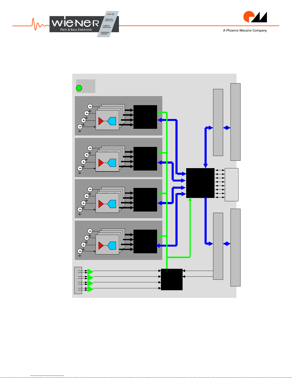
The AVM-16 / AVX-16 modules contain four quad-channel ADC blocks, a VME / VXS control
part and a clock and synchronization utility, see figure 1.
Figure 1:AVM-16 / AVX-16 design overview. Please note that the SYNCH section is meant
customizations. Only the external trigger input is present on all boards.
AMP+ADC
AMP+ADC
AMP+ADC
AMP+ADC
Feature
extraction
FPGA
AMP+ADC
AMP+ADC
AMP+ADC
AMP+ADC
Feature
extraction
FPGA
AMP+ADC
AMP+ADC
AMP+ADC
AMP+ADC
Feature
extraction
FPGA
AMP+ADC
AMP+ADC
AMP+ADC
AMP+ADC
Feature
extraction
FPGA
Control
FPGA
P1
P2
P0
SYNCH
SIGNAL INPUTS (LEMO)
Clock
MUX
CLK
SYNC
TRG
PRE_TRG
CLK
SYNC
Clock, Synch, Trigger &
Data Local Bus
Data Local Bus
VME Bus
VME Bus
VME interface
VME interface
Status
LED
AVM-16 / AVX-16
Page 7

7
Each of the ADC channel is equipped with a symetrizing amplifier, anti-aliasing filter and an
individual 12-bit Analog-to-Digital converter running at 160 Msamples/s.
After conversion, the digital data is passed to 4 FPGA circuits providing buffers for data retention
and a feature extraction logic. One Spartan-3 FPGA from Xilinx is used for a block of four
channel keeping a history of 1024 samples for each channel in it’s internal registers. Feature
extraction algorithms are used for calculate important parameters of the input pulses, such as
amplitude, time, intergrals and many others, which allows for minimizing of the readout data
volume and thus increasing the readout speed. The user may still choose to read a full set of
samples, recorded in the buffer or read s ubset of those samples within specified time boundaries,
being in relation to the trigger.
After a trigger request from a Data acquisition system, the stored and/or extracted data is passed to
a control FPGA chip via four Data Local Busses and then transferred over a VME bus or a VXS
backplane P2P connection fabric.
In multichannel systems, where a common time base is required, a global clock and
synchronization signals are provided over a front panel connector or over a non-legacy user VME
connector pins. The clocking and synchronization circuitry allows for choosing of the clock
source.
Page 8
8
3 Input circuitry
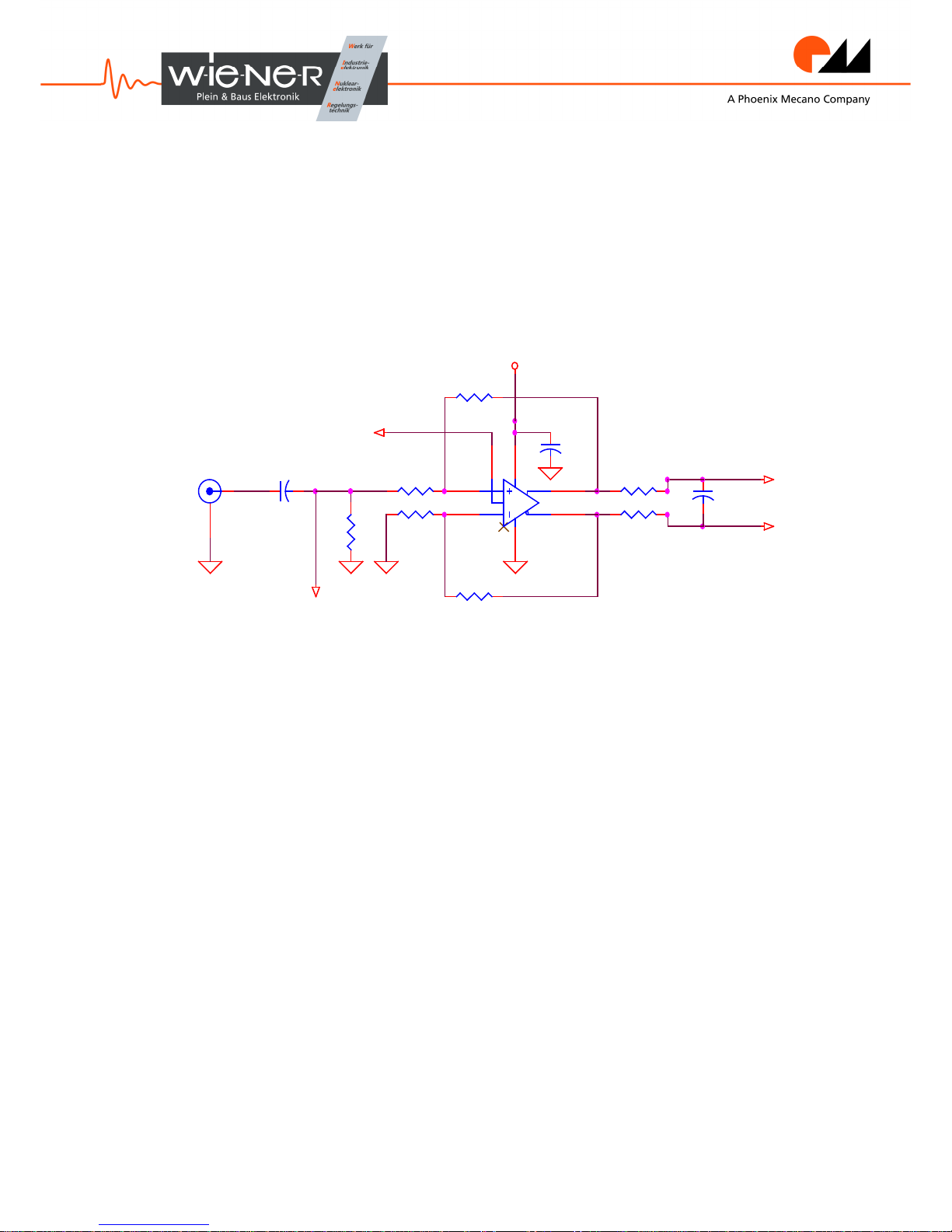
The input AC filter provides an effective cut-off for bacground low frequency noise and mains
pick-up. DC coupling is possible on demand. The symmetrizing amplifiers provide a differential
input for the ADC circuits, reducing PCB noise pickup. The anti-aliasing filter allows for precise
parametrization of input pulses as short as 10 ns FWHM. The anti-aliasing filter can be
customized or removed by the manufacturer or by an authorized person, see figure 2.
An on-board pulse generator provides test pulses for every channel.
R1
51
1
2
3
4
5
6
7
8
V+
V-
Vcm
U1
AD8132AR
R5 51
R7 51
R3
1k
R6
510
R4
510
R2
1k
C1
100nF
C2
C_fil
C3
100nF
VCC
TEST PULSE
COMMON LEVEL
1
2
J1
BNC
ADCp
ADCn
Figure 2: Input symetrizing amplifier and anti-aliasing filter (R5, R7, C2). The gain
resistors, the location of the test pulse and the values and locations of capacitors may
depend on AVM16 version or be customized.
Page 9
9
4 Triggering
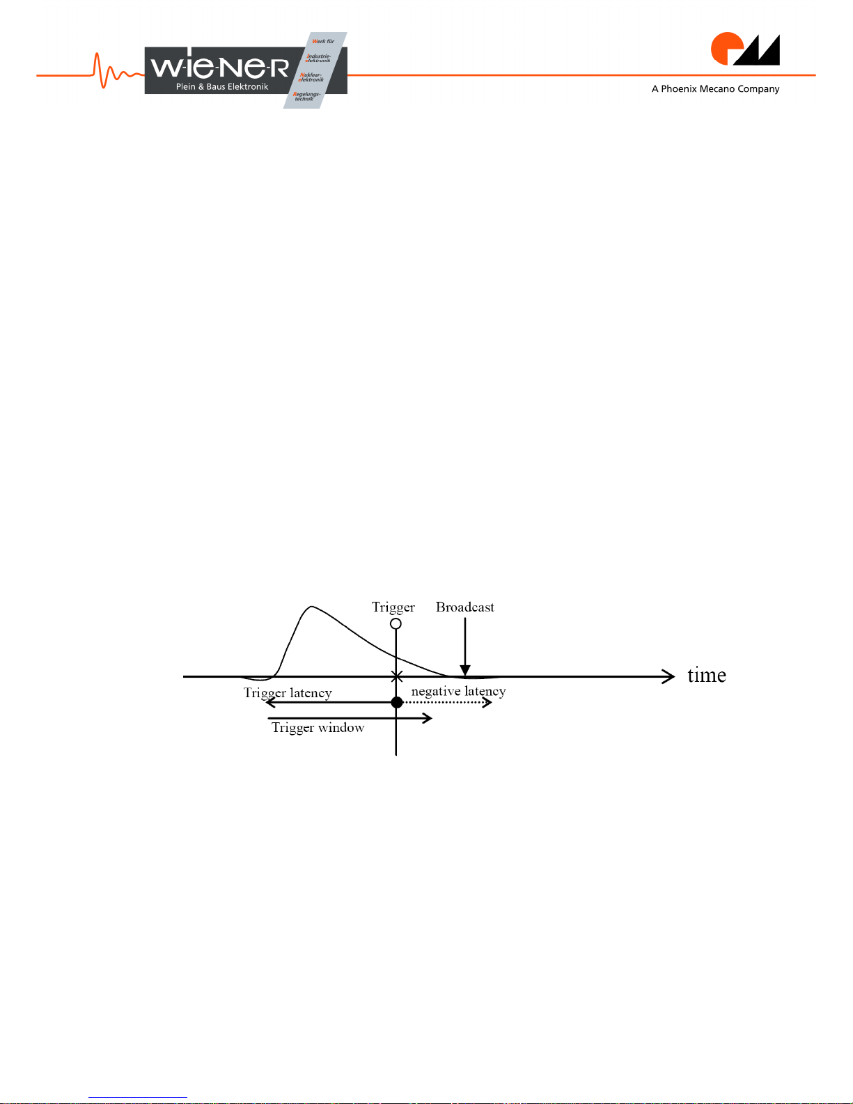
AVM16 / AVX16 can either be trigger internally or externally. The external trigger time is
distributed via a broadcast command. Trigger time is used to set time boundaries for scanning the
Dual-Ported RAM’s, given user defined trigger latency and trigger window, see figure 3.
The trigger source configuration is in register 0x100.
4.1 Internal trigger functionality
When the signal in one of the non inhibited channels overcomes the trigger level set in the register
0x110 with reference to the actual baseline, all non inhibited channels are read out. The trigger
condition is
ADC_VALUE > BASE_LINE + TRIGGER_LEVEL
and is checked at 80 MHz rate, each time for two samples sequentially. The trigger uncertainty is
thus +/- 1 sample, corresponding to a range of 12.5 ns.
4.2 External trigger functionality
All non inhibited channels are read out when a LVDS singal is feed into the TRG port on the front
panel.
4.3 Software trigger
All non inhibited channels are read out upon write on bit 2 of register 0x104
Figure 3: Data window for feature extraction
Page 10
10
5 Technical description of AVM-16 / AVX-16
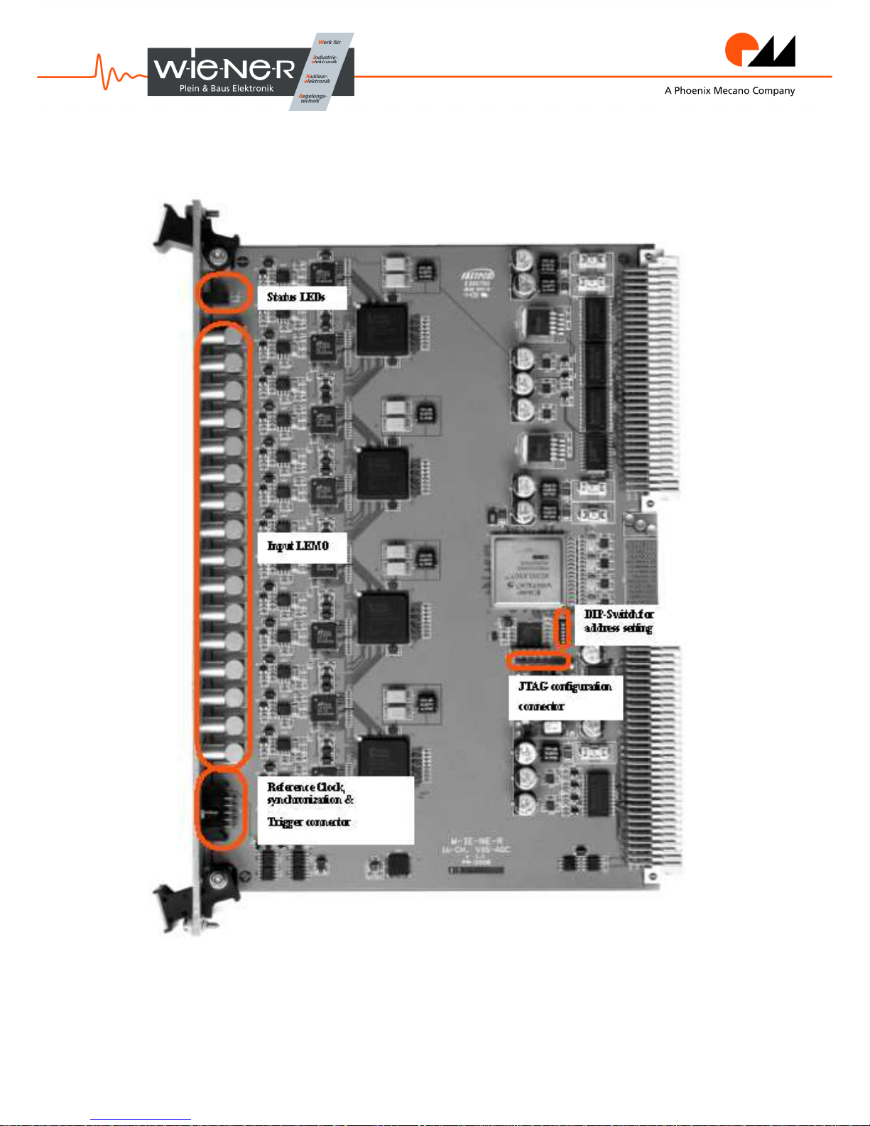
Figure 6. shows location of key connectors user may interface to
Figure 4: The AVM-16 / AVX-16 Printed circuit board
Page 11
11
5.1 Technical description
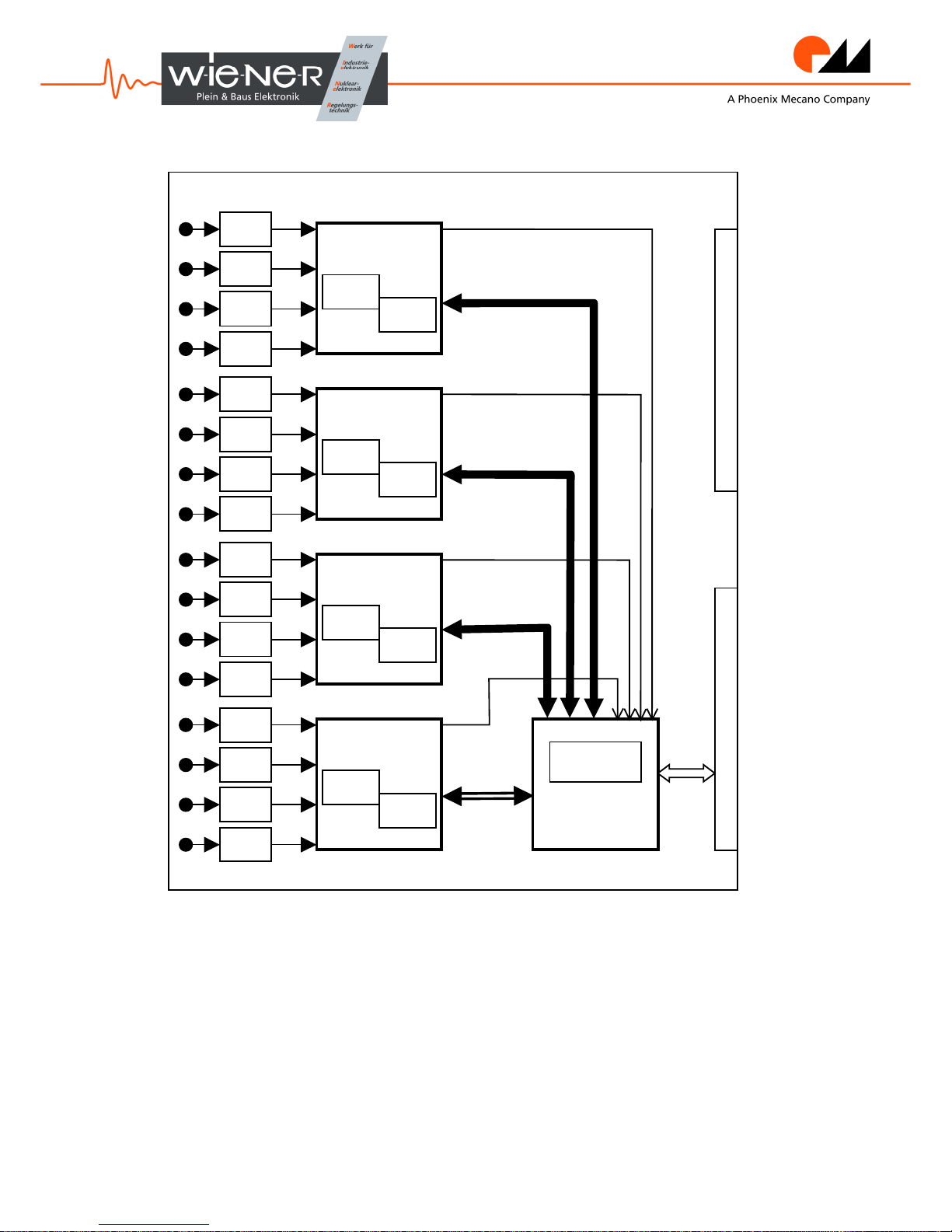
AVM16/AVX16 works with a sampling frequency of 160 MHz. ADC chips are LTC2240 with 12
Bit resolution. The input circuit differential amplifier is AD8132. The coupling is capacitive, thus
the baseline is situated in the middle of the measurement range.
The logic is implemented on 4 SPARTAN-3 FPGAs, each one serving 4 ADCs, and one
VIRTEX-5 Control FPGA as interface between the 4 ADC FPGAs and the VME Bus. The
Control FPGA is VIRTEX-5 XC5VLX50T. The FPGAs serving the ADCs are SPARTAN-3
XC3S1000.
ADC
ADC
ADC
ADC
DPRAM
FIFO
4 x
XC3S1000
ADC
ADC
ADC
ADC
DPRAM
FIFO
4 x
XC3S1000
ADC
ADC
ADC
ADC
DPRAM
FIFO
4 x
XC3S1000
ADC
ADC
ADC
ADC
DPRAM
FIFO
4 x
XC3S1000
gateway
XC5VLX50T
Data Request
P2 VME BUS
P1 VME BUS
Data Bus
Figure 5: Chips diagram
Page 12
12
5.2 FPGA logic
Data storage and the feature extraction are implemented in programmable logic circuits (FPGA).
Each of the FPGAs handles data from 4 ADC channels.
5.2.1 Window control
After detection of a trigger, the corresponding time stamp is sent to all ADC FPGAs. With this
time stamp the trigger window is determined and all data in the DPRAM within this window are
retrieved and analysed.
5.2.2 Feature Extraction
To maximize readout speed and minimize the amount of data, the AVM and AVX devices are
equipped with feature extraction algorithms, which instantly calculate important parameters of the
input signal. Raw data readout is still available for debugging purposes.
The data coming contiuously from ADC convertes are stored in ring buffers (Dual-Ported RAM),
keeping a record of the last 1024 samples from each channel. Samples are tagged with an internal
time of the ADC module, which is synchronized to a global clock by signals coming via either
external connectors on each device or by a signal distributed on dedicated user lines of the VME
bus (present on request).
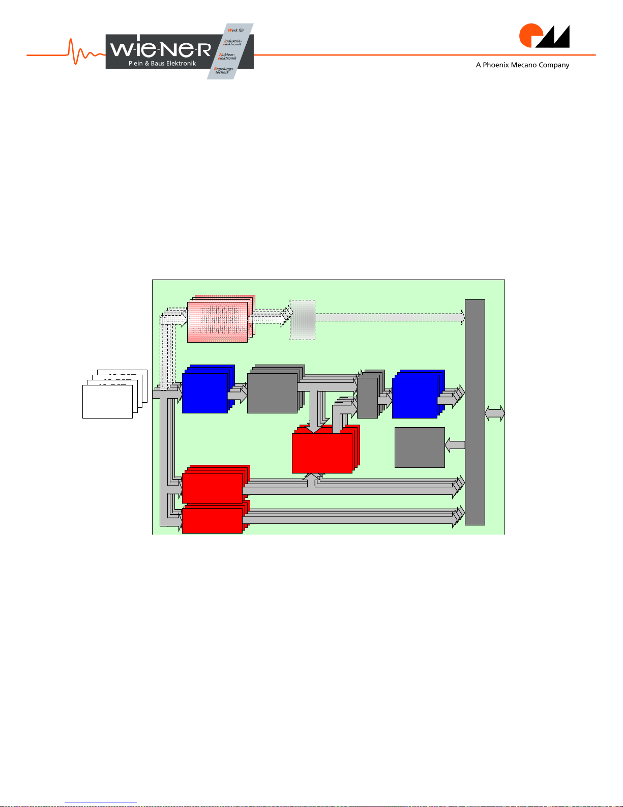
Data from within the boundaries of the window control are transferred to the Waveform Feature
Extraction section and (if raw data are requested) also to readout FIFOs. A list of extracted
parameters is given in figure 5.
Pulse integrals can be calculated within fixed time windows (absolute times relative to the trigger)
or in floating windows (relative to the pulse leading edge and within a specified number of
samples). Data is validated by comparing integrals of signals with thresholds, individual for each
channel.
12-BIT
ADC
12-BIT
ADC
12-BIT
ADC
12-BIT
ADC
LOCAL
BUS
(data+
trigger+
timing)
TRIGGER BUS
(VXS Version)
LOCAL BUS INTERFACE
DPRAM
WINDOW
CONTROL
FIFO
WAVEFORM
ANALYSIS
PEDESTAL
EXTRACTION
NOISE PP
M
U
X
CONTROL
DPRAM
WINDOW
CONTROL
FIFO
WAVEFORM
ANALYSIS
PEDESTAL
EXTRACTION
NOISE PP
M
U
X
DPRAM
WINDOW
CONTROL
FIFO
WAVEFORM
ANALYSIS
PEDESTAL
EXTRACTION
NOISE PP
M
U
X
DPRAM
WINDOW
CONTROL
FIFO
WAVEFORM
FEATURE
EXTRACTION
PEDESTAL
EXTRACTION
NOISE PP
M
U
X
TRIGGER
FEATURE
EXTRACTION
TRIGGER
FEATURE
EXTRACTION
TRIGGER
FEATURE
EXTRACTION
TRIGGER
FEATURE
EXTRACTION
M
U
X
Figure 6: Feature extraction FPGA
Page 13
13
Extracted parameters fill the remaining part of the readout FIFOs and in case of valid data, readout
request signals are issued.
A Trigger Feature Extraction algorithm delivers instant integrals and times for trigger purposes. It
is only available in AVX-16 version, prepared for the VXS standard. Extracted parameters are
transferred to a VXS data processor for evaluation of advanced trigger decisions.
The feature extraction and data transfers can ether be triggered internally or by a dedicated pretrigger signal delivered from a trigger system via a dedicated front panel connector.
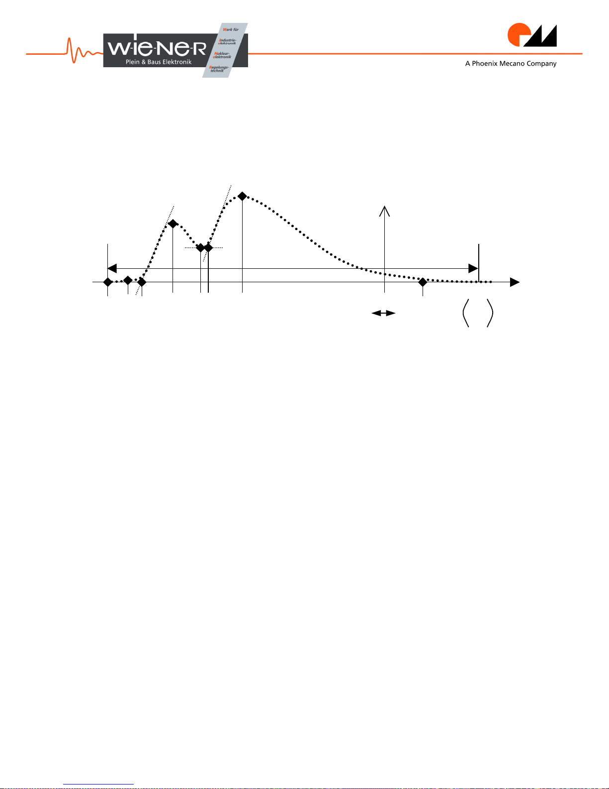
P0 – window beginning
Pi – time for the first non-zero value
Pz – pulse start time calculated from slope crossing the pedestal value
Pa – signal amplitude
Pq – signal integral (charge) *
PPi – minimum value before pileup
PPz – pileup pulse start time calculated from slope crossing the momentary pedestal value Ppi
PPa – pileup pulse amplitude
Pe – pileup integral, starting from PPi
* If pileup occurs, the integral Pq is only calculated untill PPi time
5.3 VME addressing
AVM16/AVX16 reacts to
A32/D32 write and read accesses with Address Modifiers (AM)
0x09/0x0D, to A32/D32 Block Transfer (BLT) with AM 0x0B/0x0F and to A32/D64
Block Transfer (MBLT) with AM 0x08/0x0C. The base address
is set by means of a 6 fold
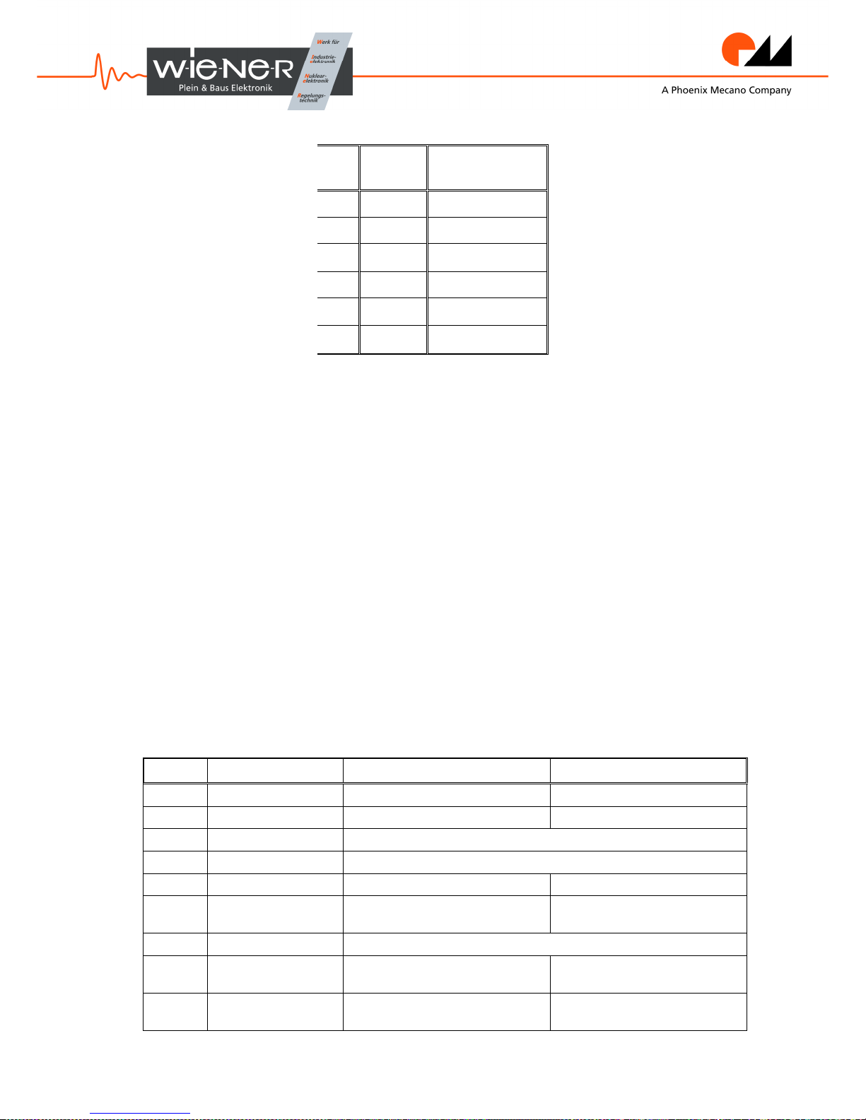
DIP Switch SW1 according to Table 1
trigger
window
time
time=0
+
-
P0 Pi Pz PPa PPi PPz PPq Pe
Pq
Pa
Pq
Figure
7: Feature extraction parameters
Page 14
14
A switch in the „on“ position means that the corresponding address bit should be 0. Address bits
25:11 must always be 0. If for example only switch 1 is „off“, the address range is 0x04000000 to
0x040007FC.
5.4 Software registers
There are 4 groups of address registers:
• The first contains only registers for the control FPGA VIRTEX-5, i.e. the local bus is not
used
• The second contains registers that are also passed through the local bus to all 4 FPGAs
serving the ADCs.
• The third contains registers that contain values for each one of the 16 channels and
address the corresponding ADC FPGA.
• The range of the fourth group is foreseen for access to the readout data in single mor in
block transfer mode.
The meaning and functions of the internal registers is listed in paragraphs below.
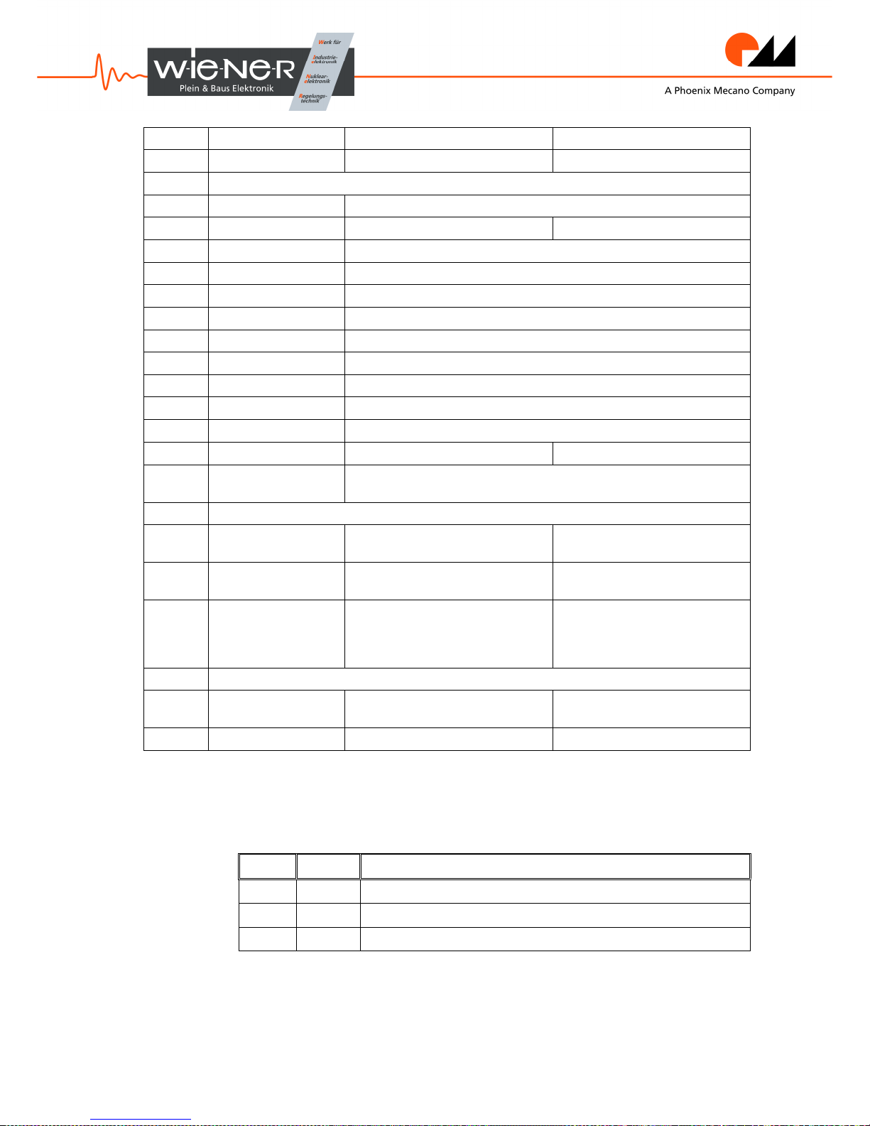
5.4.1 Overview of registers
Offset Name Write Read
0x000 ident
Version
0x004 serial
serial number, 32 Bit
0x008 com_ids
communication identifier
0x00C
reserved
0x010 state
Status Register
0x014 dlength
Data Length for
Blocktransfer as Byte
0x018
reserved
0x01C tp_dac
Level of test pulse
(DAC)
0x020 ofset_dac[4]
baseline offset for all
ADC inputs
SW1 Bit Base Address
6 31 0x80000000
5 30 0x40000000
4 29 0x20000000
3 28 0x10000000
2 27 0x08000000
1 26 0x04000000
Table 1: Base Address Settings
Page 15
15
0x030 jtag_csr
JTAG Control JTAG Status
0x034 jtag_data
JTAG runtest JTAG Data
reserved
0x100 cr
Control/Mode Register
0x104 act
action like Master Reset
0x108 cha_inh
disable single channels, 16 Bit
0x10C cha_raw
set channel to raw mode, 16 Bit
0x110 trg_level
local trigger level, 12 Bit
0x114 anal_ctrl
signal analyzing control
0x118 iw_start
start of integral window, 10 Bit
0x11C iw_length
length of integral window, 10 Bit
0x120 sw_start
start of pulse search window, 10 Bit signed
0x124 sw_length
length of search window, 9 Bit
0x128 sw_intlength
length of integral of the signal analyzing
0x12C aclk_shift
step phase shift factor status
0x1300x13C
lb_test[4]
rw test register for the local bus (to 4
SPARTAN's)
reserved
0x2000x23C
base_line[16]
auto base line 12 bit
0x2400x27C
noise_level[16]
peak to peak noise
level, 5 Bit
0x2800x2BC
q_threshold[16]
Q-Threshold for
transmitting the
integral data of the
integral window
reserved
0x4000x7FC
data_range
data, single or block
transfer
5.4.2 First group of registers (control FPGA)
ident 0x000 - Board Id. Contains firmware version number.
Bit Value Meaning
7:0 0x70
AVM16 Module Id
15:8 0x01
Firmware Version (here 0.1)
31:16 0
Reserved
serial 0x004 - User serial number. This number can be programmed by the user and is
saved in the FPGA PROMs. Read and write access possible.
Page 16
16
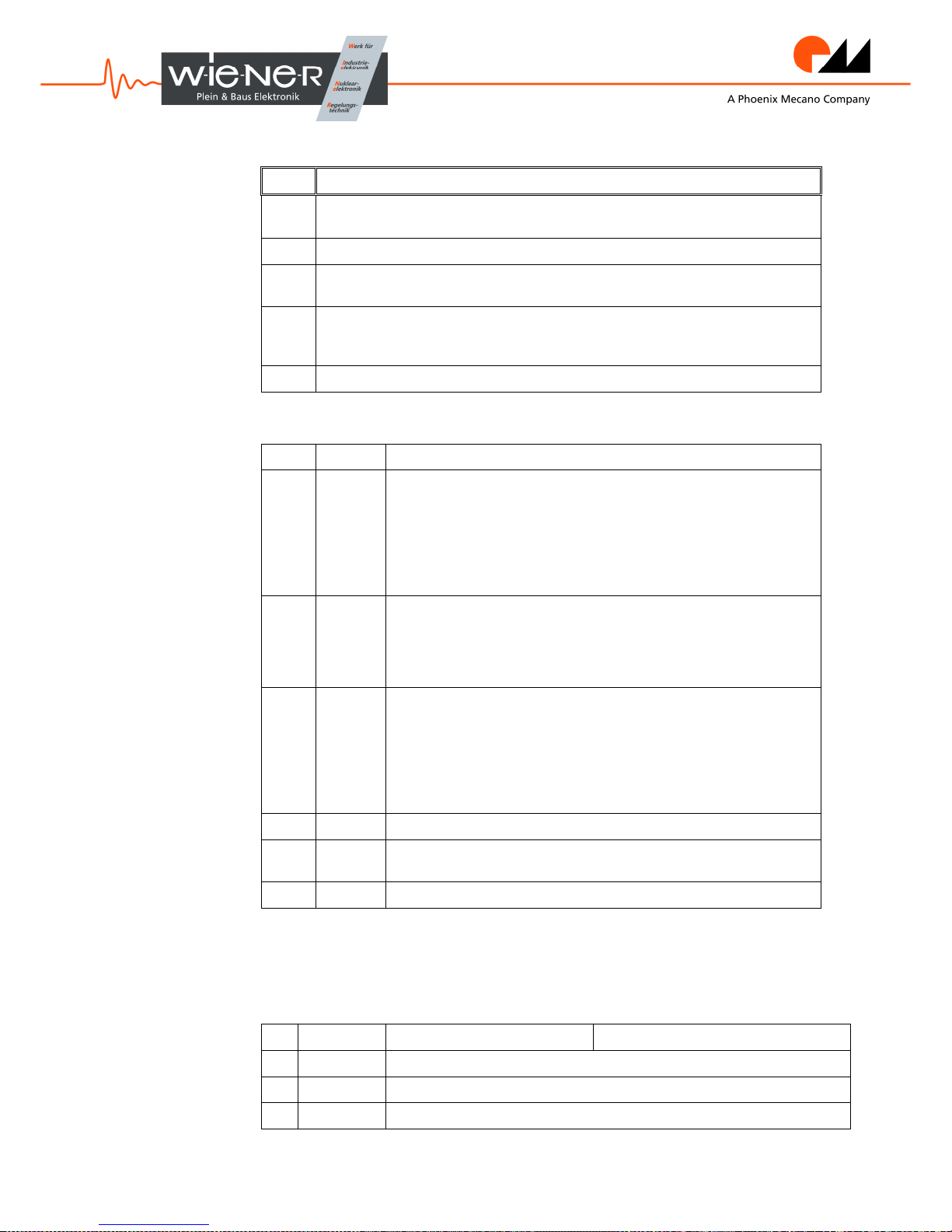
com_ids 0x008 - In this register there are three identifiers for communication.
Bit Meaning
2:0
Interrupt Request Level (1 to 6) an interrupt is issued
if data are available. A 0 disables the interrupt
7:3
Null
15:8
Interrupt Vector, it is transmitted on Interrupt
Acknowledge in order to identify the interrupt
19:16
Data recognition. These 4 bits are written in bit 31:28
of data, so that it is possible to map data to a
specific module (see data format)
31:20
Null
state 0x010 - General Status Register
Bit Name Meaning
0 DVAL
Data valid: data are ready in VIRTEX-5. If this
bit is set an interrupt is triggered in case the
programmed Interrupt Level is not zero. Only
when all data have been read, more data (that
may have been triggered meanwhile) from the ADC
FPGAs can be loaded. The number of bytes is in
dlength register.
1 DAVAL
Data available, compared to the DVAL bit, this
bit is already set when the first word is
present in a FIFO. DVAL is only set when all
data were written in the FIFOs and thus the
dlength register is valid.
2 ROBUSY
This bit is set when a trigger is fired,
blocking further triggers. It is only reset when
all data in the FIFOs are read out. As long as
old data are present in a FIFO, this bit remains
set. This means that the readout data still
cannot be transmitted from the ADC Spartan FIFOs
to the VIRTEX-5 FIFOs.
3
Null
7:4 LTSRC
Level Trigger Source, indicates which ADC
channel fired the last level trigger.
31:8
Null
dlength 0x014 - This register indicates how many bytes are present in the FIFOs (in total).
For each ADC SPARTAN-3 is a FIFO available. By readout FIFO 0 (channel 0 to
3) has the higher priority. A FIFO can store 32 kB (8k values).
jtag_csr 0x030 - JTAG control/status Register
Bit Name Write Read
0
TDI Data Input to the first JTAG device
1
TMS Mode Select
2
TCK JTAG Clock, must be zero when AUTO_CLK is used
Page 17
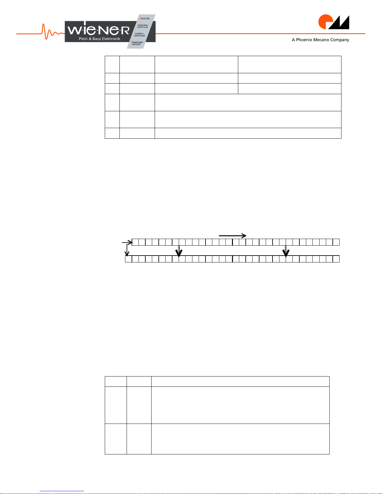
17
3
TDO Data Output of the last JTAG
device
4
RTEST JTAG runtest is running
7:5
8
ENABLE drives signal to the JTAG Connector, the connector
must be free
9
AUTO_CLK one clock cycle is generated, rising and falling
edge
With bit 8 set TDI, TMS and TCK in JTAG connector are driven from FPGA.
Otherwise these signals are high impedance, in order for an external
programming tool to be able to connect. By means of this register it is possible to
enable a program to gain full control over the JTAG chain.
jtag_data 0x034 - This register has two functions:
a) With the read function the user gets the shift register for TDO. In orden not to
have to read jtag_csr after each output, the TDO bit is moved to a write
register with each cycle, so that the last 32 TDO bits (e. g. Device ID) can be
read out in chain.
b) With the write function a number of TCK Clocks with TMS=0 is returned.
The value is used in svf Files as "RUNTEST n TCK". In this way it is possible
to insert pauses after commands.
tp_dac 0x01C - With bit 3 in “act” register it is possible to generate a test pulse through a
DAC. The height of the test pulse is set by means of this td_dac register. Since the
DAC has 8 bits, only bits 11:4 are relevant.
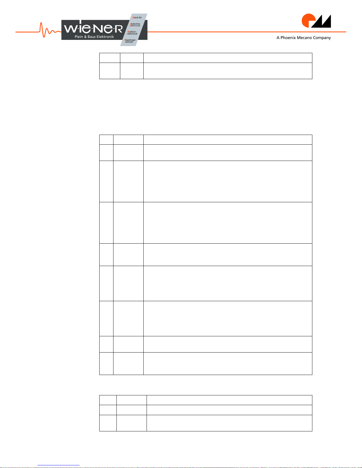
offset_dac[4] 0x020 - (Not in all AVM16 version implemented). When no signal is connected,
the ADC mean output value is about 0x800, i.e. a signal in one polarity can use
only half of the measurement range. By means of an offset value for a DAC, it is
possible to reduce this ADC mean value until zero. For this purpose there are 4
DACs with 12 bit each for 4 channels. The DAC (AD5324) has the following
register assignments:
Bit Name Function (WO)
11-0 DATA
12 bit fffset, one unit corresponds to about one
ADC unit, i.e. when the value here is increased
by 0x100, the ADC mean value when no signal is
present should decrease more or less by the same
value.
12 nLDAC
If this bit is 0, all 4 channels are updated.
Otherwise, the data value is only temporarily
saved with no effect. This bit is always set to 0
internally.
30 15 16 0 TDO
31 15 16 0
TCK shift
jtag_data
Page 18
18
13 nPD
"not power down", this bit is set internally to 1
15-14 A1/A0 Channel number 0 to 3 for ofs_dac[0], 4 to 7 for
ofs_dac[1] and so on...
5.4.3 Registers that are sent to all ADC FPGAs too.
The readback of these registers occurs from a shadow register in VIRTEX-5.
cr 0x100 - Control/Mode Register
Bit Name Function
0 ENA
General enable. If this bit is not set, AVM16 is
in its groud state. All data are deleted.
1 EXTRIG
Enables the trigger input from the front
connector (LVDS). The trigger time is determined
in VIRTEX-5 and sent to all ADC FPGAs, in order
to start the analysis. The next trigger is then
only possible when all data have been transmitted
to VIRTEX-5.
2 LEVTRIG
With this bit a trigger is fired when the value
of an ADC input (that is not inhibited by cha_inh
) overcomes the value in trig_level register. The
corresponding ADC FPGA sends the trigger time to
VIRTEX-5 which forwards it to all ADC FPGAs in
order to start the read out.
3 VERBOSE
When this bit is set, the pairs of values for
minima and maxima are transmitted (if RAW Mode is
not set).
4 ADCPOL
The polarity of the ADC data can be changed here.
By default are ADC data inverted, to analyze
negative pulses. When this bit is set, ADC data
are not inverted, to analyze positive pulses.
Also the RAW data are invereted.
5 SGRD
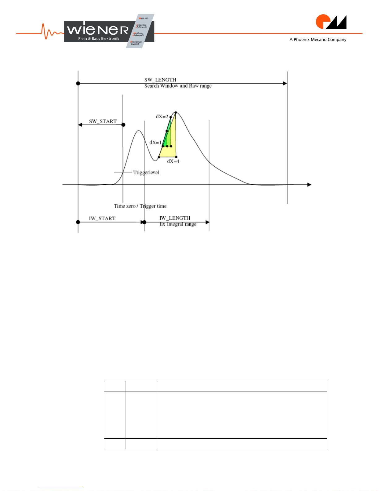
Single Gradient. In the computation of the rise
time only two points with ∆x=1 are considered.
Normally ∆x can also be 2 or 4, if the
corresponding y values lie between ¼ and ¾ of the
maximal value.
6 TP_ON
With this bit the test signal can be statically
enabled.
7 PW_ON
With this bit, the analog ADC power supply can be
statically enabled. Otherwise, it is only enabled
when bit 0 (ENA) is set.
act 0x104 - Action register
Bit Name Write/single shot
0 MRST
Master Reset
1 SRST
Synchron Reset for all timers, so that all FPGAs
have the same time reference.
Page 19
19
2 TRIGGER
Software Trigger
3 TPULSE
Generates a test pulse of 25 ns
cha_inh 0x108 - The corresponding channel to each bit (0 bis 15) which is set is inhibited.
cha_raw 0x10C - If the corresponding channel to each bit is set all ADC data that are
within WINDOW are transmitted and afterward all available analysis data
(including start, min and max pairs).
trig_level 0x110 - This value is the trigger level when bit 2 in cr register is set. Internally,
the actual baseline value is added to this value.
anal_ctrl 0x114 - Here it is possible to parametrize the pulse analysis:
Bit Default Function
3..0 8 Integral based detection:
this value times 4 indicates how high should
the integral be in order for a pulse to be
detected. In case of pile up the integral is
computed on the basis of the last minimum
value.
11..8 1 Distance from another maximum:
number of clock units after the last maximum
(start time point) from where a new pulse (even
a pile up) can be detected.
The default values are restored by reset or by writing 0. Zero as parameter is not
valid.
iw_start 0x118 - Begin of the supplementary integral window in the search-main window.
The time unit is the ADC sample rate (6,25 ns). The value must be bigger or equal
4, in order for the 4 values leading the window to be present for calculating the
pedestal.
iw_length 0x11C - Length of the integral window in units of the ADC clock. The end of the
integral windows plus 4 should not overcome the end of the main window. The
time unit is the ADC sample rate (6,25 ns).
sw_start 0x120 - (Trigger latency) Begin of the time window for the trigger time search
range. The value is subtracted from the trigger time and thus defines the beginning
of the time window. The range is -512 to 511 times 12,5 ns (±6,4 µs). A negative
value means trigger time before window.
sw_length 0x124 - Length of the time window. The time corresponds to the value plus 1
times 12,5 ns. The maximum value is 511, i.e. 6,4 µs.
Summary of constraints to be respected:
IW_START >= 4
IW_START + IW_LENGTH + 4 <= 2 * SW_LENGTH;
sw_intlength 0x128 - Integral length of pulse integrals in ADC sample rate units (6,25 ns). After
a reset the value is set to maximum (0x03FF). By default (i.e. with the maximum
value) the pulse integral is computed over the total pulse length. In case of pile
up, each pulse integration starts from the minimum before the peak and ends in the
Page 20
20
minimum between the peaks, where the integral for next peak starts, or by
reaching the baseline level for the last peak. With the value in this register it is
possible to end the integration earlier when the number of bins reaches the value.
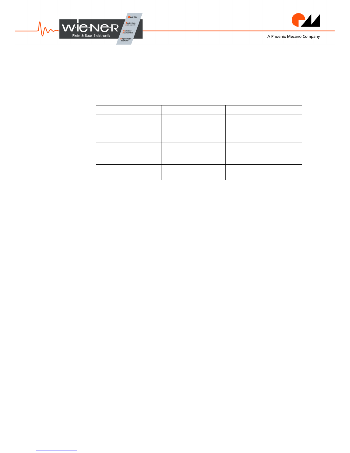
aclk_shift 0x12C - The ADC clock must have a fixed phase to the FPGA clock, in order to
correctly transmit ADC data. For test purposes it is possible to change the phase,
e.g. in order to determine whether the default phase is set correctly. The default
phase is 0.
Bit ADC Write Read
0
4
8
12
3..0
7..4
11..8
15..12
Execute a step Step executed
1,5,9,13 dto.
0 for positive
step and 1 for
negative step
Upper or lower limit
reached, overflow
2,6,10,14 dto.
Reset number of
steps to 0
0
160 steps in one or the other direction correspond to ±180°.
lb_test[4] 0x130 to 0x13C - Every one of the 4 SPARTAN-3 FPGAs has a data test register,
for testing the local data bus. These registers should be writable with any 16 bit
value and it should be possible to read this value back.
5.4.4 Registers that are individually available for every channel.
base_line[16] 0x200 to 0x23C - In the FPGA the ADC mean value for each channel is
computed continuously. ADC input test pulses are excluded.
noise_level[16] 0x240 to 0x27C - In the FPGA the noise amplitude is computed for each
channel, by subtracting the minimum value from the maximum value.
Since there is no expected big noise level, these registers have a 5 bit
width (max. 31 noise bins). By readout all maxima and minima are reset
to the present value. The FPGA logic is so designed that noise is not
computed for a given time before and after an input pulse.
q_threshold[16] 0x280 to 0x2BC - The computed data from the integral window are only
delivered if the corresponding integral is higher than the value of this
register. If the value is 0 data are always delivered. Read back is not
possible.
5.4.5 Registers for data readout in single or block transfer mode.
data_range 0x400 to 0x7FC - ADC/QDC data stored in VIRTEX-5 FIFO can be read out
through this address, independently from which address in this range is read, so
that also an incremental block transfer is possible. Single transfers as well as block
transfers BLT and MBLT are allowed.
Page 21
21
Figure 8: graphical representation of configuration parameters with details of dX
5.5 Decoding output
The output can be verbose or compact, depending on the value of the cha_raw register for each
channel individually. Each 32 bit double word is made of one label, the first word, an one value,
the second word.
In the raw data in verbose mode, the label is the channel number and the value is the sample. In
the extracted features, the labels indicate the physical meaning of the word that follows, according
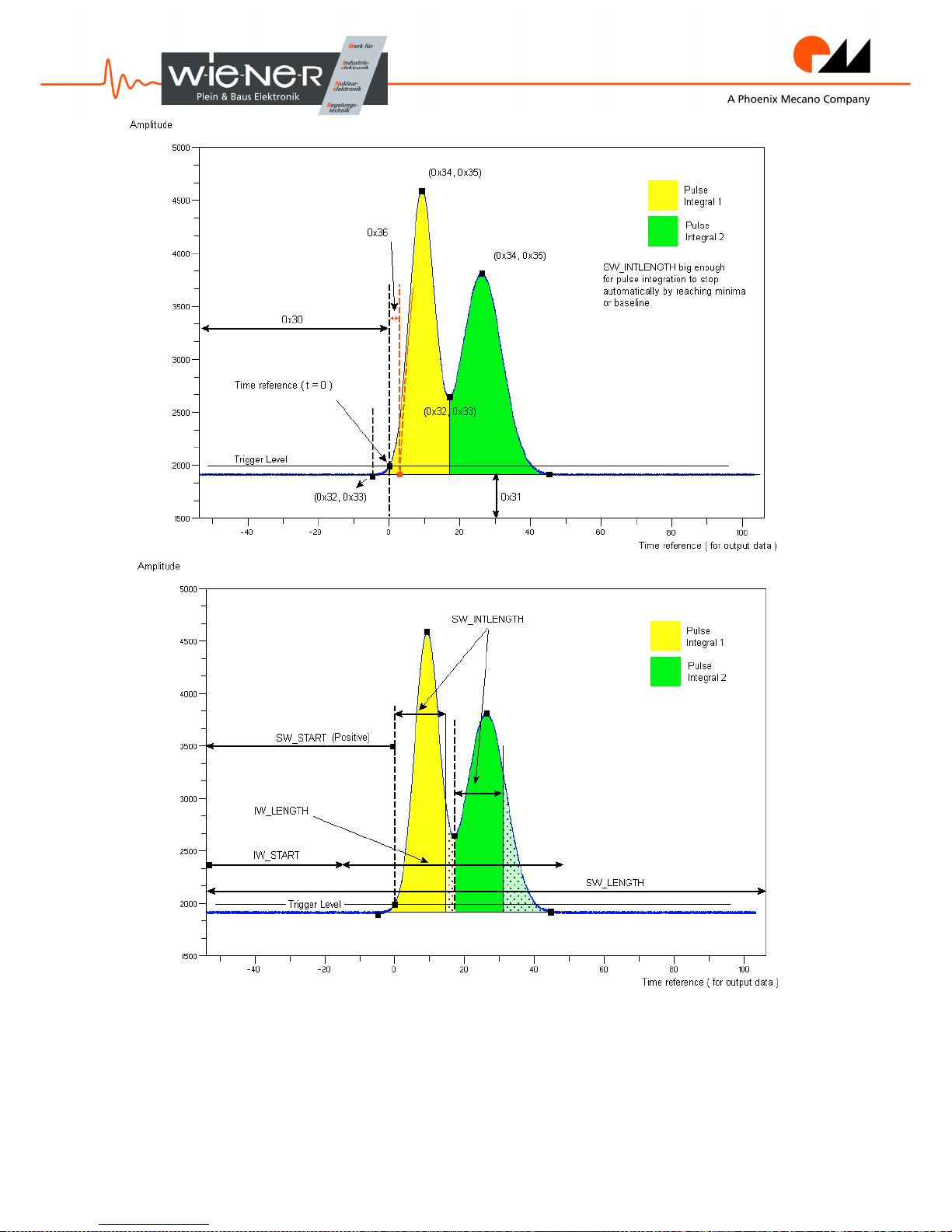
to the following list for the first channel (channel 0):
• Label 0x30: window start time (first value), referred to the trigger time (that is the time
reference and corresponds to t = 0 ) or window end (value before the last one)
• Label 0x31: mean level, zero point of ADC data (updated continuously as long as no trigger is
fired)
Maxima, minima:
By means of register 0x114 it is possible to parametrize the pulse analysis:
Bit Default Function
3..0 8 Integral based detection:
this value times 4 indicates how high should
the integral be in order for a pulse to be
detected. In case of pile up the integral is
computed on the basis of the last minimum
value.
11..8 1 Distance from another maximum:
Page 22

22
number of clock units after the last maximum
(start time point) from where a new pulse (even
a pile up) can be detected.
Maxima and minima computed according to parametrization are found in
• Label 0x32: minimum time
• Label 0x33: minimum level
• Label 0x34: maximum time
• Label 0x35: maximum level, bit 19 is used to indicate overflow.
Pulse arrival time (zero crossing) and derivative are given as
• Label 0x36: zero crossing, bit 15:14 are used for ∆X:
• 00 => ∆X =1 bin
• 01 => ∆X =2 bins
• 10 => ∆X =4 bins
• bit 13 determines the sign. Negative means before the trigger (t = 0).
For each peak, the first derivative is computed in the middle point between maximum and baseline
(for pile up peaks the last minimum is used instead of the baseline) using 1, 2 and 4 bins. The
choosen value corresponds to the biggest ∆X for which
¼ h < ∆Y < ¾ h
where h is the peak heigth. From the first derivative, the zero crossing time point is extrapolated.
• Label 0x37 indicates the beginning of a block of 4 values with data describing
the integral window. This block is transmitted at the beginning of the features
extraction data and contains the following information:
• 1st value 0x37: instant mean line level (updated continuously as long as no
trigger is fired).
This value is identical to 0x31
• 2nd value 0x37: mean value of the 4 samples before the integral window
• 3rd value 0x20: integral on the whole user parametrized integral window (IW)
• 4th value 0x37: mean value of the 4 samples following the integral window
Page 23
23
Figure 9: upper picture: graphical representation of the extracted features. Lower picture: input
parameters with details on SW_INT_LENGTH
Page 24
24
• Label 0x20 (outside 0x37 block): pulse integral in case of pile up. The integral starts
from the last minimum before the peak and ends when the level of that minimum or
the baseline is reached, unless it is stopped earlier by the user defined parameter
SW_INTLENGTH
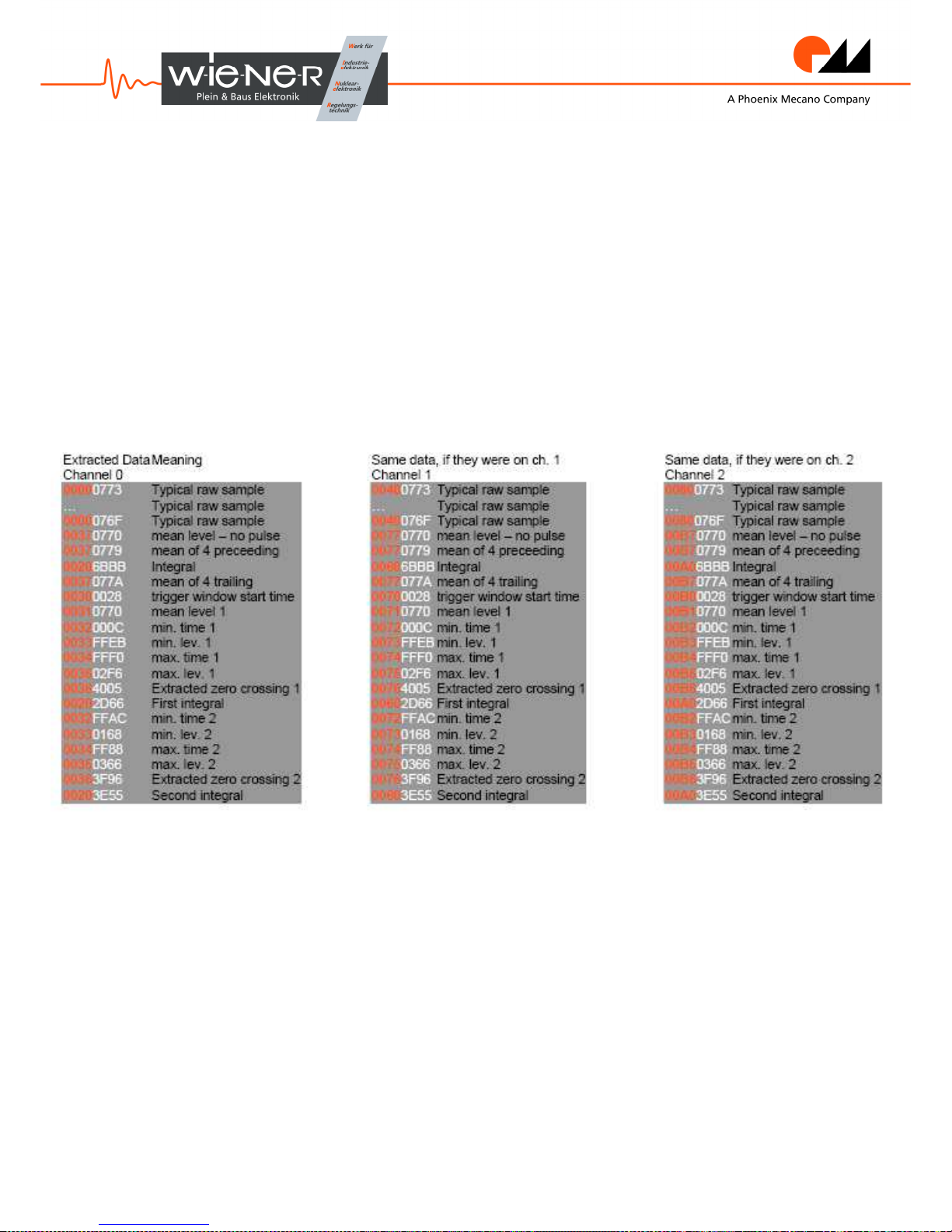
Note: all labels refer to channel 0. In order to decode labels for other channels, following
formula applies:
Label for channel 0 (e.g. 0x37) + 4 * 0x10 * (channel number)
Example: label 0x037 for channel 2 is: 0x037 + 4 * 2 * 0x10 = 0x0B7
label 0x037 for channel 10 (0xA) is: 0x037 + 4 * 0xA * 0x10 = 0x2B7
Practical example for decoding AVM16 data:
Figure 10: representation of the data analysis output
Page 25
25
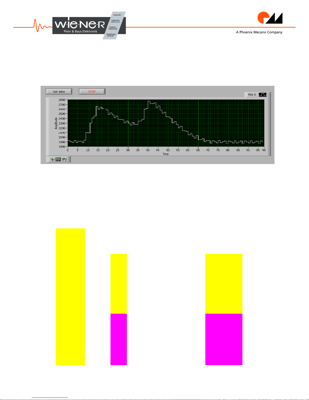
5.6 Example of data readout
This examples helps to understand the data analysis and shows how data are extracted from the
raw data samples. Data were taken in channel 0.
Sample
Raw value
Time
Hex Dec
Absolute
abs. Hex
Register/
Value
In 1,5625ns
units
Used in calculations
1 78E 28 30 -> #028
2 770 24
3 762 20
4 78B 1C 78B 1931 27 001B
Mean of
5 761 18 761 1889 -15 FFFFFFFFF1 4 preceeding
6 77C 14 77C 1916 12 000C 779
7 77C 10 77C 1916 12 000C
8 75B min. 1 C
75B
1883 -21 FFFFFFFFEB 32 -> #00C
9
793 8
793
1939 35 0023 33 -> #FEB
10 82D 4
82D
2093 189 00BD
Figure 11: Example of raw data (pileup event with small noise peaks)
Page 26
26
11 827 0
827
2087 183 00B7
12 8FF FFC
8FF
2303 399 018F
13 968 FF8
968
2408 504 01F8
14 997 FF4
997
2455 551 0227
15 A66 peak 1 FF0
A66
2662 758 02F6 34 -> #FF0
16 A24 FEC
A24
2596 692 02B4 35 -> #2F6
17 A59 FE8
A59
2649 745 02E9
18 A38 FE4
A38
2616 712 02C8
19 A2D FE0
A2D
2605 701 02BD First integral
20 A14 FDC
A14
2580 676 02A4 11622
21 9B5 FD8
9B5
2485 581 0245 2D66 20 -> 2D66
22 9D5 FD4
9D5
2517 613 0265
23 9A8 FD0
9A8
2472 568 0238
24 975 FCC
975
2421 517 0205
25 994 FC8
994
2452 548 0224
26 94F FC4
94F
2383 479 01DF
27 94D FC0
94D
2381 477 01DD
28 945 FBC
945
2373 469 01D5
29 904 FB8
904
2308 404 0194
30 929 FB4
929
2345 441 01B9
31 901 FB0
901
2305 401 0191
32 8D8 min2 FAC
8D8
2264 360 0168 32 -> #FAC
33 90E FA8
90E
2318 414 019E 33 -> #168
34 8E7 FA4
8E7
2279 375 0177
35 8E1 FA0
8E1
2273 369 0171
36 929 F9C
929
2345 441 01B9
37 92E F98
92E
2350 446 01BE
38 952 F94
952
2386 482 01E2
39 A24 F90
A24
2596 692 02B4
40 A3F F8C
A3F
2623 719 02CF
41 AD6 peak 2 F88
AD6
2774 870 0366 34 -> #F88
42 AA5
AA5
2725 821 0335 36 -> #366
43 AA1
AA1
2721 817 0331
44 AB3
AB3
2739 835 0343
45 A4D
A4D
2637 733 02DD
Page 27

27
46 A73
A73
2675 771 0303
47 A10
A10
2576 672 02A0
48 9D0
9D0
2512 608 0260
49 9E6
9E6
2534 630 0276 Second integral
50 986
986
2438 534 0216 15957
51 97E
97E
2430 526 020E 3E55 20 -> 3E55
52 960
960
2400 496 01F0
53 905
905
2309 405 0195
54 923
923
2339 435 01B3
55 8E1
8E1
2273 369 0171
56 89E
89E
2206 302 012E
57 8BB
8BB
2235 331 014B
58 862
862
2146 242 00F2
59 85D
85D
2141 237 00ED
60 855
855
2133 229 00E5
61 802
802
2050 146 0092
62 81A
81A
2074 170 00AA
63 7E5
7E5
2021 117 0075
64 7BB
7BB
1979 75 004B
65 7EF
7EF
2031 127 007F
66 79B
79B
1947 43 002B
67 79B
79B
1947 43 002B
68 7B3
7B3
1971 67 0043
69 778
778
1912 8 0008
70 78E 78E 1934 30 001E Mean of
71 784 784 1924 20 0014 4 trailing
72 750 750 1872 -32 FFFFFFFFE0 1914,5
73 788 788 1928 24 0018 077A 37 -> #77A
74 770
75 78A
76 75A
77 772
78 77F
79 74D
80 781
81 770
82
755
83 785
Page 28

28
84 758
85 76E
86 77F
87 74A
88 782
89 76D
90 755
91 785
92 759
93 76D
94 77B
95 74C
96 780
97 76A
5.6.1 Sample column
In the “sample” column there is simply the index of the value read out from the FIFO (registers:
data_range). In this example we have 97 samples, corresponding to a value of 0x30 (in decimals:
48) of window length (see sw_start and sw_length registers).
5.6.2 Raw data column
Here we have the data as read out from the FIFO. Maxima and minima are highlighted. Only the
data in this column and the analysis data (see 5.5) are read out from AVM16.
5.6.3 Time column
Here we have the time at which the corresponding raw data value was sampled. This values were
not read out from the ADC, they were added manually basing on the “window start time” value.
The window start time is part of the data analysis and can be read out from the FIFO after the raw
data block, if raw data are present, or directly (see 5.5).
5.6.4 Hex column
This column is a repetition of the raw data column, with background colours indicating for which
parameter calculation (integral, average…) the data are used.
5.6.5 Dec column
This colums translates the values of the hex column into decimals, so that we can easily verify the
calculations made by the FPGA.
5.6.6 Absolute column
Here there are the same values as in the dec column, pedestal subtracted. The pedestal is the
“mean level” value from the data analysis (see 5.5), in this example it is 0x770, i.e. 1904 in
decimals.
Page 29
29
5.6.7 Absolute hex
Translation of absolute column into hex.
5.6.8 Register value
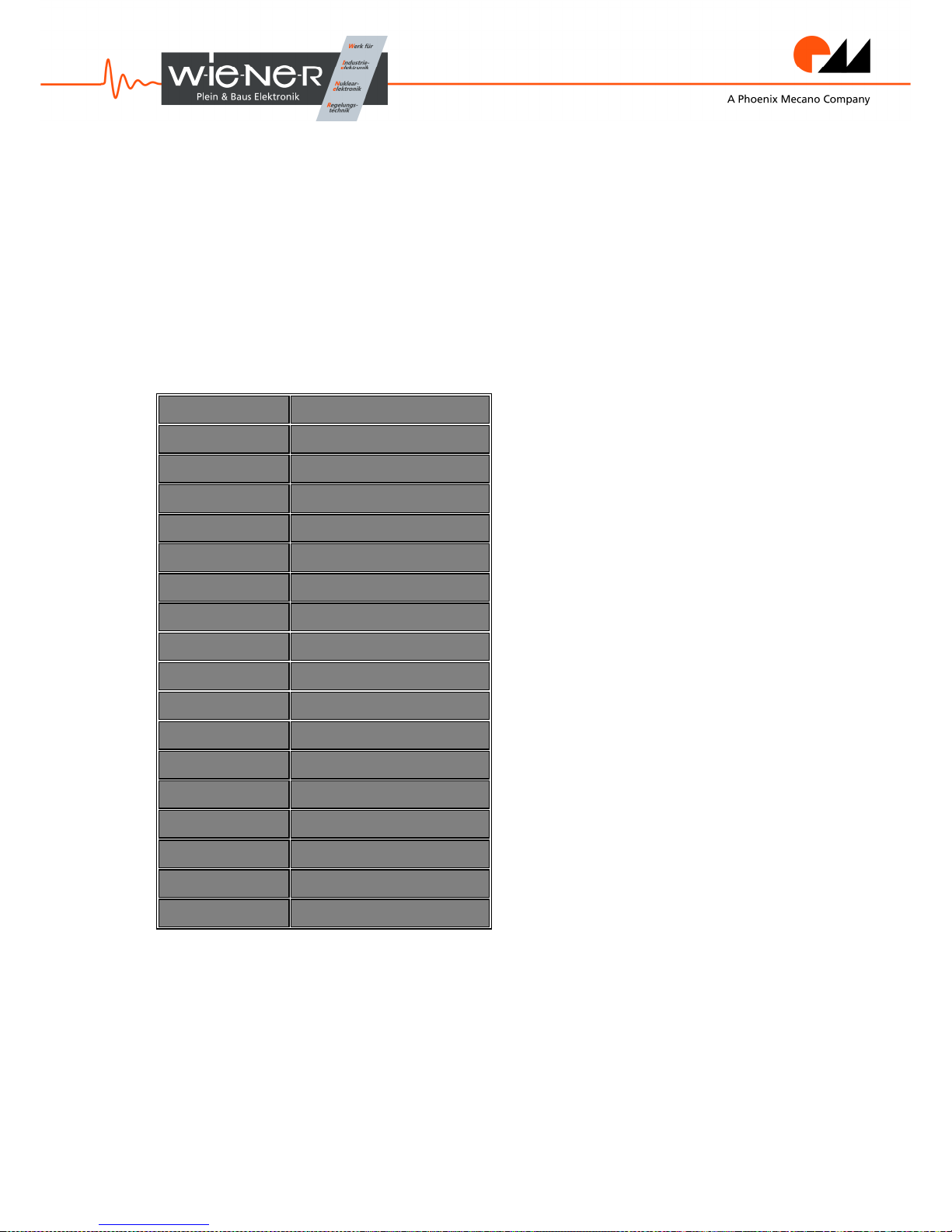
Shows the relationship between the data computed by the FPGA and the raw data. This is to verify
if the FPGA correctly inferred timing and values of maxima and minima as well as integrals,
averages and zero crossing times.
Extracted Data
Meaning
370770 mean level
370779 mean of 4 preceeding
206BBB Integral
37077A mean of 4 trailing
300028
trigger window start time
310770 mean level 1
32000C min. time 1
33FFEB min. lev. 1
34FFF0 max. time 1
3502F6 max. lev. 1
364005
Extracted zero crossing 1
202D66 First integral
32FFAC min. time 2
330168 min. lev. 2
34FF88 max. time 2
350366 max. lev. 2
363F96
Extracted zero crossing 2
203E55 Second integral
Page 30

30
Page 31

User’s Manual AVM16 / AVX16
W-Ie–Ne-R
Plein & Baus GmbH
September 10 31
Page 32

Page 33

User’s Manual AVM16 / AVX16
W-Ie–Ne-R
Plein & Baus GmbH
September 10 33
 Loading...