

Datasheet WE128K32P-300G4Q, WE128K32P-300G4MA, WE128K32P-300G4M, WE128K32P-300G4IA, WE128K32P-300G4I Datasheet (White Electronic Designs)
...
1
White Electronic Designs Corporation • (602) 437-1520 • www.whiteedc.com
HI-RELIABILITY PRODUCT
WE128K32-XXX
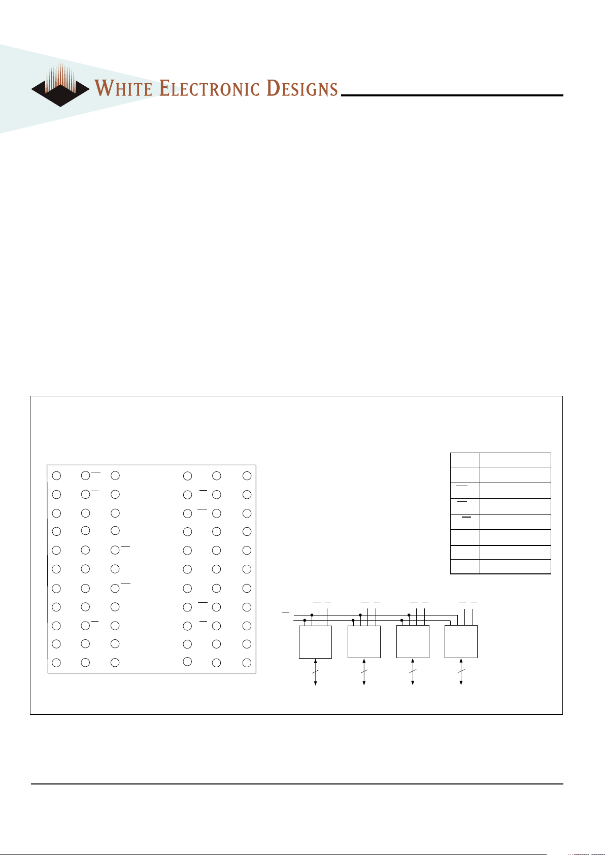
128Kx32 EEPROM MODULE, SMD 5962-94585
TOP VIEW
PIN DESCRIPTION
I/O0-31 Data Inputs/Outputs
A0-16 Address Inputs
WE1-4 Write Enables
CS1-4 Chip Selects
OE Output Enable
VCC Power Supply
GND Ground
NC Not Connected
BLOCK DIAGRAM
I/O
8
I/O
9
I/O
10
A
13
A
14
A
15
A
16
NC
I/O
0
I/O
1
I/O
2
WE
2
CS
2
GND
I/O
11
A
10
A
11
A
12
V
CC
CS
1
NC
I/O
3
I/O
15
I/O
14
I/O
13
I/O
12
OE
NC
WE
1
I/O
7
I/O
6
I/O
5
I/O
4
I/O
24
I/O
25
I/O
26
A
6
A
7
NC
A
8
A
9
I/O
16
I/O
17
I/O
18
V
CC
CS
4
WE
4
I/O
27
A
3
A
4
A
5
WE
3
CS
3
GND
I/O
19
I/O
31
I/O
30
I/O
29
I/O
28
A
0
A
1
A
2
I/O
23
I/O
22
I/O
21
I/O
20
11 22 33 44 55 66
1 12 23 34 45 56
128K x 8
8
I/O
0-7
CS
1
128K x 8
8
I/O
8-15
2
128K x 8
8
I/O
16-23
3
128K x 8
8
I/O
24-31
4
A
0-16
OE
WE
CS
WE
CS
WE
CS
WE
1234
FEATURES
■ Access Times of 120*, 140, 150, 200, 250, 300ns
■ Packaging:
• 66-pin, PGA Type, 27.3mm (1.075") square, Hermetic
Ceramic HIP (Package 400)
• 68 lead, 40mm CQFP (G4), (Package 501)
• 68 lead, 22.4mm sq. CQFP (G2T), 4.57mm (0.180") high,
(Package 509)
• 68 lead, 22.4mm sq. Low Profile CQFP (G1U), 3.57mm
(0.140") high, (Package 519)
■ Organized as 128Kx32; User Configurable as 256Kx16 or 512Kx8
■ Write Endurance 10,000 Cycles
■ Data Retention Ten Years Minimum (at +25°C)
■ Commercial, Industrial and Military Temperature Ranges
■ Low Power CMOS
■ Automatic Page Write Operation
■ Page Write Cycle Time: 10ms Max
■ Data Polling for End of Write Detection
■ Hardware and Software Data Protection
■ TTL Compatible Inputs and Outputs
■ 5 Volt Power Supply
■ Built-in Decoupling Caps and Multiple Ground Pins for Low
Noise Operation
■ Weight
WE128K32-XG2TX - 8 grams typical
WE128K32-XG1UX - 5 grams typical
WE128K32-XH1X - 13 grams typical
WE128K32-XG4X - 20 grams typical
* 120ns not available for SMD product
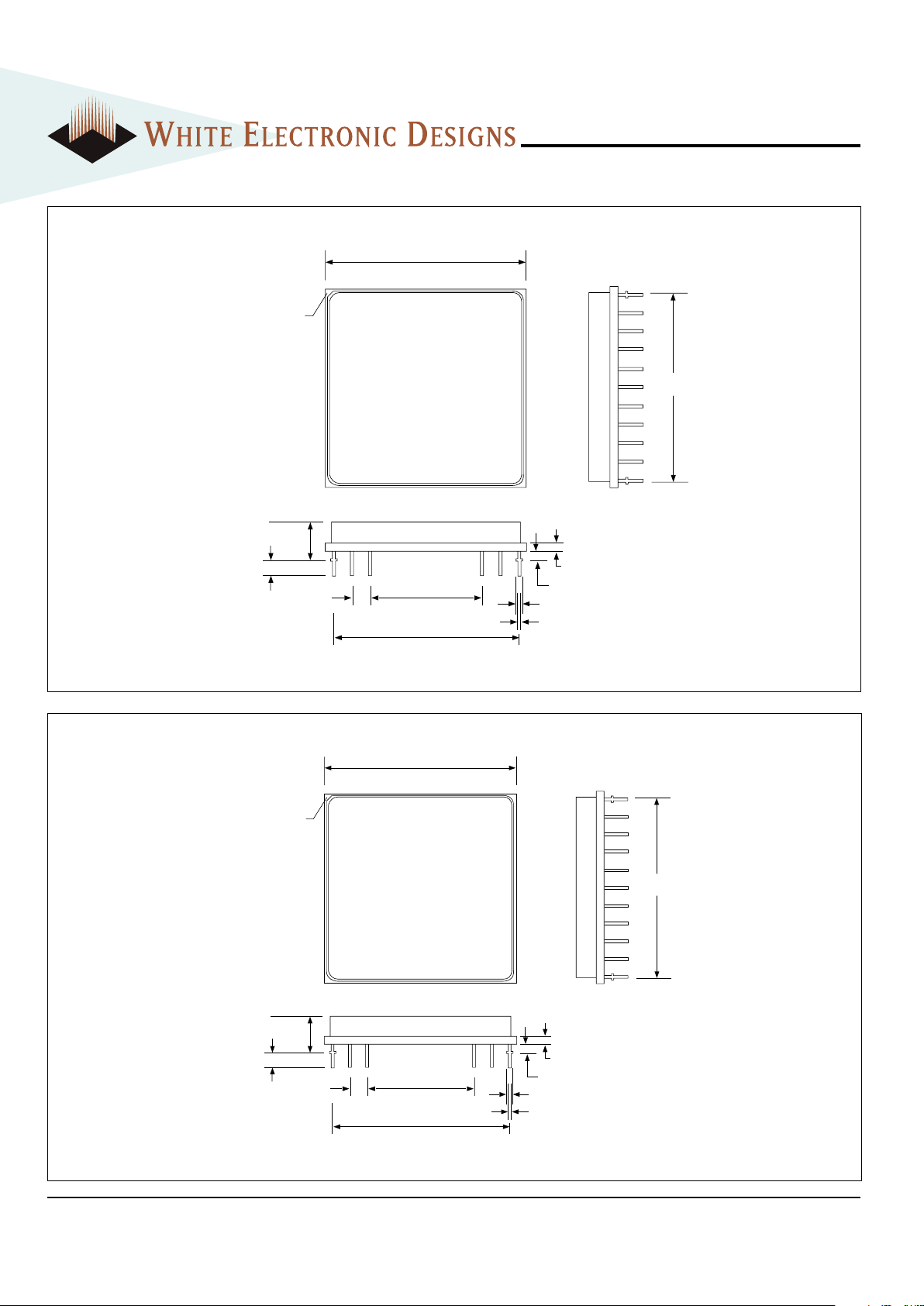
FIG. 1 PIN CONFIGURATION FOR WE128K32N-XH1X
July 2001 Rev. 5
2
White Electronic Designs Corporation • (602) 437-1520 • www.whiteedc.com
WE128K32-XXX
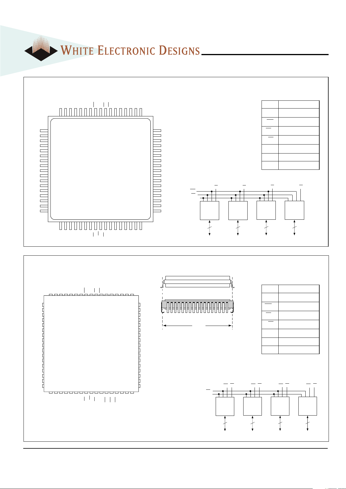
FIG. 2 PIN CONFIGURATION FOR WE128K32-XG4X
10
11
12
13
14
15
16
17
18
19
20
21
22
23
24
25
26
60
59
58
57
56
55
54
53
52
51
50
49
48
47
46
45
44
9 8 7 6 5 4 3 2 1 68 67 66 65 64 63 62 61
27 28 29 30 31 32 33 34 35 36 37 38 39 40 41 42 43
I/O
0
I/O
1
I/O
2
I/O
3
I/O
4
I/O
5
I/O
6
I/O
7
GND
I/O
8
I/O
9
I/O
10
I/O
11
I/O
12
I/O
13
I/O
14
I/O
15
V
CC
A11A12A13A14A15A
16
CS2OECS4
NC
NC
NCNCNCNCNC
I/O
16
I/O
17
I/O
18
I/O
19
I/O
20
I/O
21
I/O
22
I/O
23
GND
I/O
24
I/O
25
I/O
26
I/O
27
I/O
28
I/O
29
I/O
30
I/O
31
NC
A0A1A2A3A4A5CS1GND
CS3WE
A6A7A8A9A10V
CC
PIN DESCRIPTION
BLOCK DIAGRAM
TOP VIEW
128K x 8
8
I/O
0-7
CS
1
128K x 8
8
I/O
8-15
CS
2
128K x 8
8
I/O
16-23
CS
3
128K x 8
8
I/O
24-31
CS
A0-
16
OE
WE
4
10
11
12
13
14
15
16
17
18
19
20
21
22
23
24
25
26
60
59
58
57
56
55
54
53
52
51
50
49
48
47
46
45
44
9 8 7 6 5 4 3 2 1 68 67 66 65 64 63 62 61
27 28 29 30 31 32 33 34 35 36 37 38 39 40 41 42 43
I/O
0
I/O
1
I/O
2
I/O
3
I/O
4
I/O
5
I/O
6
I/O
7
GND
I/O
8
I/O
9
I/O
10
I/O
11
I/O
12
I/O
13
I/O
14
I/O
15
V
CC
A11A12A13A14A15A
16
CS
1
OE
CS
2
NC
WE
2WE3WE4
NC
NC
NC
I/O
16
I/O
17
I/O
18
I/O
19
I/O
20
I/O
21
I/O
22
I/O
23
GND
I/O
24
I/O
25
I/O
26
I/O
27
I/O
28
I/O
29
I/O
30
I/O
31
NC
A0A1A2A3A4A5CS3GND
CS4WE1A6A7A8A9A10V
CC
PIN DESCRIPTION
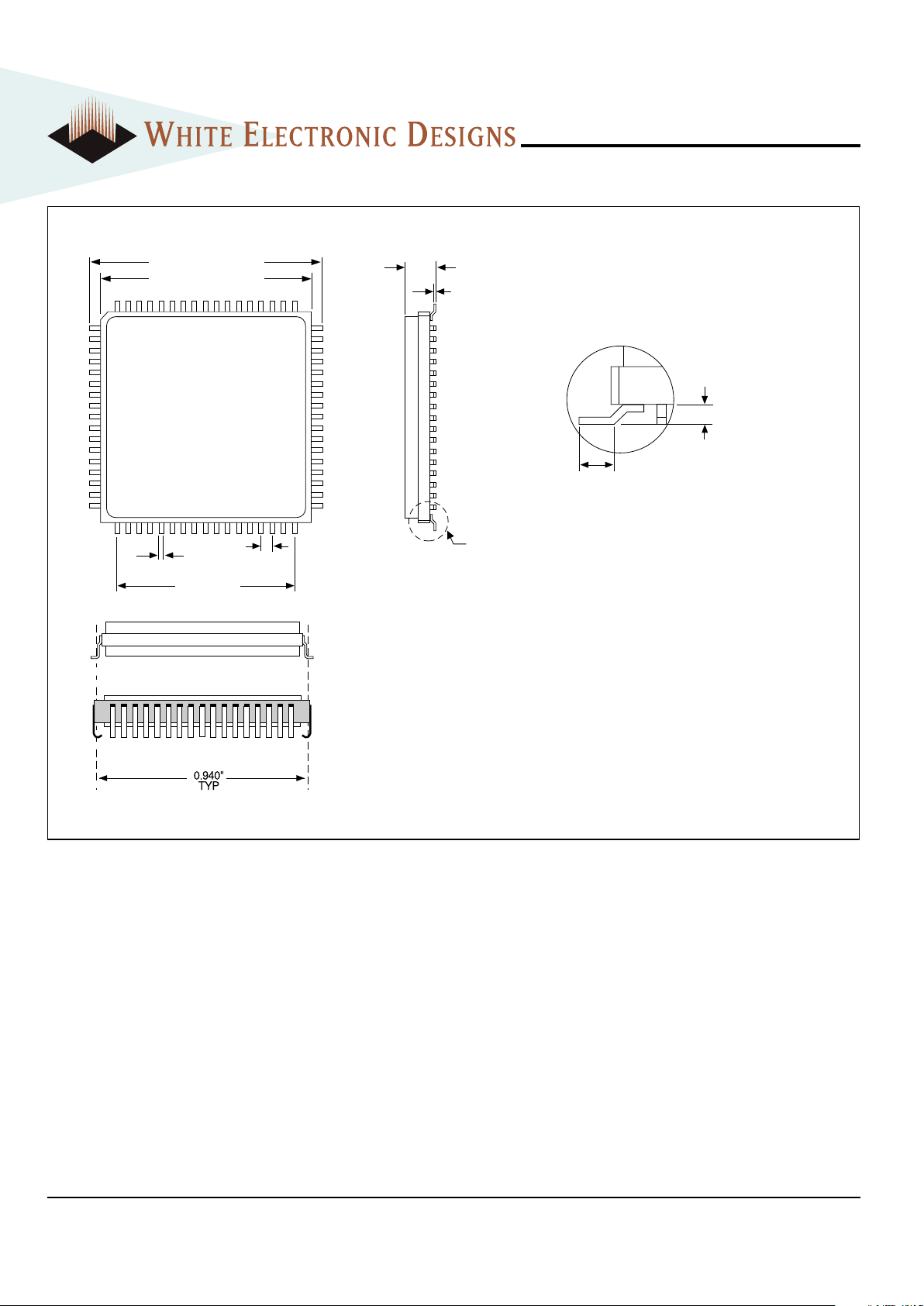
FIG. 3 PIN CONFIGURATION FOR WE128K32-XG2TX AND WE128K32-XG1UX
BLOCK DIAGRAM
128K x 8
8
I/O
0-7
CS
1
128K x 8
8
I/O
8-15
2
128K x 8
8
I/O
16-23
3
128K x 8
8
I/O
24-31
4
A
0-16
OE
WE
CS
WE
CS
WE
CS
WE
1234
TOP VIEW
The White 68 lead G2T/G1U
CQFP fills the same fit and
function as the JEDEC 68 lead
CQFJ or 68 PLCC. But the G2T/
G1U has the TCE and lead
inspection advantage of the
CQFP form.
I/O0-31 Data Inputs/Outputs
A0-16 Address Inputs
WE1-4 Write Enables
CS1-4 Chip Selects
OE Output Enable
VCC Power Supply
GND Ground
NC Not Connected
I/O0-31 Data Inputs/Outputs
A0-16 Address Inputs
WE Write Enables
CS1-4 Chip Selects
OE Output Enable
VCC Power Supply
GND Ground
NC Not Connected
0.940"
3
White Electronic Designs Corporation • (602) 437-1520 • www.whiteedc.com
WE128K32-XXX
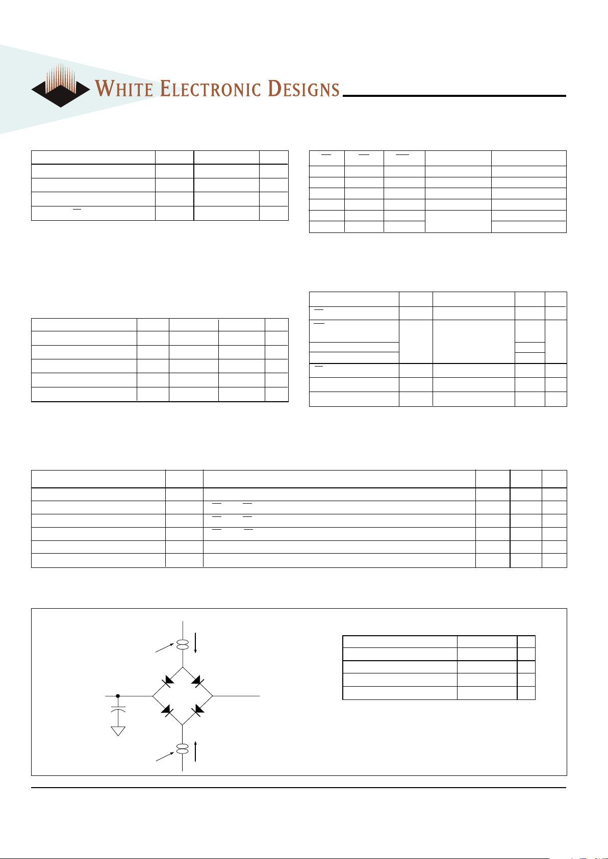
ABSOLUTE MAXIMUM RATINGS TRUTH TABLE
FIG. 4
AC TEST CIRCUIT
AC TEST CONDITIONS
I
Current Source
D.U.T.
C = 50 pf
eff
I
OL
V ≈ 1.5V
(Bipolar Supply)
Z
Current Source
OH
NOTES:
V
Z is programmable from -2V to +7V.
I
OL & IOH programmable from 0 to 16mA.
Tester Impedance Z
0 = 75 Ω.
V
Z is typically the midpoint of VOH and VOL.
I
OL & IOH
are adjusted to simulate a typical resistive load circuit.
ATE tester includes jig capacitance.
RECOMMENDED OPERATING CONDITIONS
DC CHARACTERISTICS
(V
CC = 5.0V, VSS = 0V, TA = -55°C to +125°C)
Parameter Typ Unit
Input Pulse Levels VIL = 0, VIH = 3.0 V
Input Rise and Fall 5 ns
Input and Output Reference Level 1.5 V
Output Timing Reference Level 1.5 V
Parameter Symbol Unit
Operating Temperature TA -55 to +125 °C
Storage Temperature TSTG -65 to +150 °C
Signal Voltage Relative to GND VG -0.6 to +6.25 V
Voltage on OE and A9 -0.6 to +13.5 V
NOTE:
Stresses above those listed under "Absolute Maximum Ratings" may cause
permanent damage to the device. This is a stress rating only and functional
operation of the device at these or any other conditions above those indicated
in the operational sections of this specification is not implied. Exposure to
absolute maximum rating conditions for extended periods may affect
device reliability.
CS OE WE Mode Data I/O
H X X Standby High Z
L L H Read Data Out
L H L Write Data In
X H X Out Disable High Z/Data Out
X X H Write
X L X Inhibit
Parameter Symbol Min Max Unit
Supply Voltage VCC 4.5 5.5 V
Input High Voltage VIH 2.0 VCC + 0.3 V
Input Low Voltage VIL -0.5 +0.8 V
Operating Temp. (Mil.) TA -55 +125 °C
Operating Temp. (Ind.) T
A -40 +85 °C
Parameter Symbol Conditions Min Max Unit
Input Leakage Current ILI VCC = 5.5, VIN = GND to VCC 10 µA
Output Leakage Current ILOx32 CS = VIH, OE = VIH, VOUT = GND to VCC 10 µA
Operating Supply Current x 32 Mode ICCx32 CS = VIL, OE = VIH, f = 5MHz 250 mA
Standby Current ISB CS = VIH, OE = VIH, f = 5MHz 2.5 mA
Output Low Voltage VOL IOL = 2.1mA, VCC = 4.5V 0.45 V
Output High Voltage V
OH IOH = -400µA, VCC = 4.5V 2.4 V
NOTE: DC test conditions: V
IH = VCC -0.3V, VIL = 0.3V
CAPACITANCE
(T
A = +25°C)
Parameter
Symbol
Conditions Max Unit
OE capacitance COE
VIN = 0 V, f = 1.0 MHz
50 pF
WE
1-4 capacitance CWEVIN
= 0 V, f = 1.0 MHz
pF
HIP (PGA) 20
CQFP G4 50
CQFP G2T/G1U 20
CS1-4 capacitance CCS
VIN = 0 V, f = 1.0 MHz
20 pF
Data I/O capacitance CI/O
V
I/O
= 0 V, f = 1.0 MHz
20 pF
Address input capacitance C
AD
V
IN
= 0 V, f = 1.0 MHz
50 pF
This parameter is guaranteed by design but not tested.
4
White Electronic Designs Corporation • (602) 437-1520 • www.whiteedc.com
WE128K32-XXX
WRITE
A write cycle is initiated when OE is high and a low pulse is on WE
or CS with CS or WE low. The address is latched on the falling
edge of CS or WE whichever occurs last. The data is latched by
the rising edge of CS or WE, whichever occurs first. A byte write
operation will automatically continue to completion.
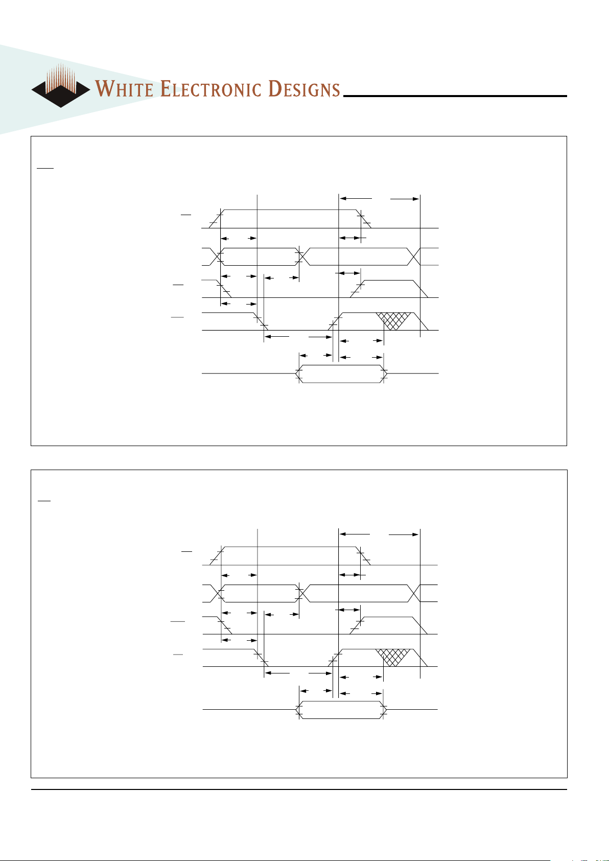
WRITE CYCLE TIMING
Figures 5 and 6 show the write cycle timing relationships. A
write cycle begins with address application, write enable and
chip select. Chip select is accomplished by placing the CS line
low. Write enable consists of setting the WE line low. The
write cycle begins when the last of either CS or WE goes low.
The WE line transition from high to low also initiates an
internal 150 µsec delay timer to permit page mode operation.
Each subsequent WE transition from high to low that occurs
before the completion of the 150 µsec time out will restart the
timer from zero. The operation of the timer is the same as a
retriggerable one-shot.
AC WRITE CHARACTERISTICS
(V
CC
= 5.0V, VSS = 0V, TA = -55°C to +125°C)
Write Cycle Parameter Symbol Min Max Unit
Write Cycle Time, TYP = 6ms tWC 10 ms
Address Set-up Time tAS 0ns
Write Pulse Width (WE or CS) tWP 150 ns
Chip Select Set-up Time tCS 0ns
Address Hold Time tAH 100 ns
Data Hold Time tDH 10 ns
Chip Select Hold Time tCSH 0ns
Data Set-up Time tDS 100 ns
Output Enable Set-up Time tOES 10 ns
Output Enable Hold Time tOEH 10 ns
Write Pulse Width High t
WPH 50 ns
5
White Electronic Designs Corporation • (602) 437-1520 • www.whiteedc.com
WE128K32-XXX
FIG. 5
WRITE WAVEFORMS
WE CONTROLLED
FIG. 6
WRITE WAVEFORMS
CS CONTROLLED
t
ADDRESS
CS
1-4
WE
1-4
DATA IN
DH
t
WPH
t
WP
t
CSH
t
OEH
t
AH
t
OES
t
AS
t
CS
OE
t
WC
t
DS
t
ADDRESS
WE1 - 4
CS1 - 4
DATA IN
DH
t
WPH
t
WP
t
CSH
t
OEH
t
AH
t
OES
t
AS
t
CS
OE
t
DS
t
WC
6
White Electronic Designs Corporation • (602) 437-1520 • www.whiteedc.com
WE128K32-XXX
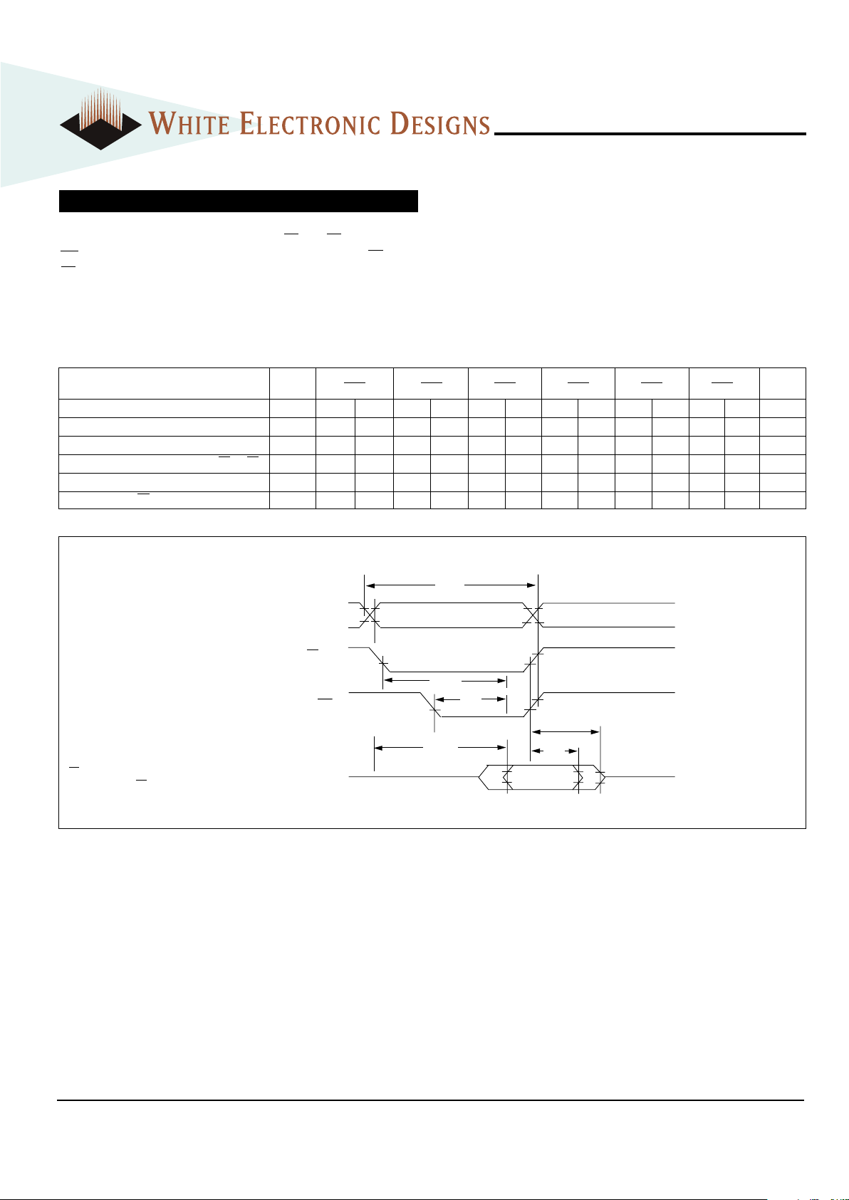
AC READ CHARACTERISTICS
(VCC = 5.0V, VSS = 0V, TA = -55°C to +125°C)
FIG. 7
READ WAVEFORMS
t
ADDRESS
CS
OE
OUTPUT
OH
t
DF
t
ACC
t
RC
t
OE
t
ACS
OUTPUT
VALID
ADDRESS VALID
HIGH Z
READ
The WE128K32-XXX stores data at the memory location
determined by the address pins. When CS and OE are low and
WE is high, this data is present on the outputs. When CS and
OE are high, the outputs are in a high impedance state. This
two line control prevents bus contention.
NOTES:
OE may be delayed up to t
ACS - tOE after the
falling edge of CS without impact on t
OE or by
t
ACC - tOE after an address change without
impact on t
ACC.
Read Cycle Parameter Symbol -120 -140 -150 -200 -250 -300 Unit
Min Max Min Max Min Max Min Max Min Max Min Max
Read Cycle Time tRC 120 140 150 200 250 300 ns
Address Access Time tACC 120 140 150 200 250 300 ns
Chip Select Access Time tACS 120 140 150 200 250 300 ns
Output Hold from Add. Change, OE or CS tOH 0 00000ns
Output Enable to Output Valid tOE 0 50 0 55 0 55 0 55 0 85 0 85 ns
Chip Select or OE to High Z Output t
DF 70 70 70 70 70 70 ns
CS1-4
7
White Electronic Designs Corporation • (602) 437-1520 • www.whiteedc.com
WE128K32-XXX
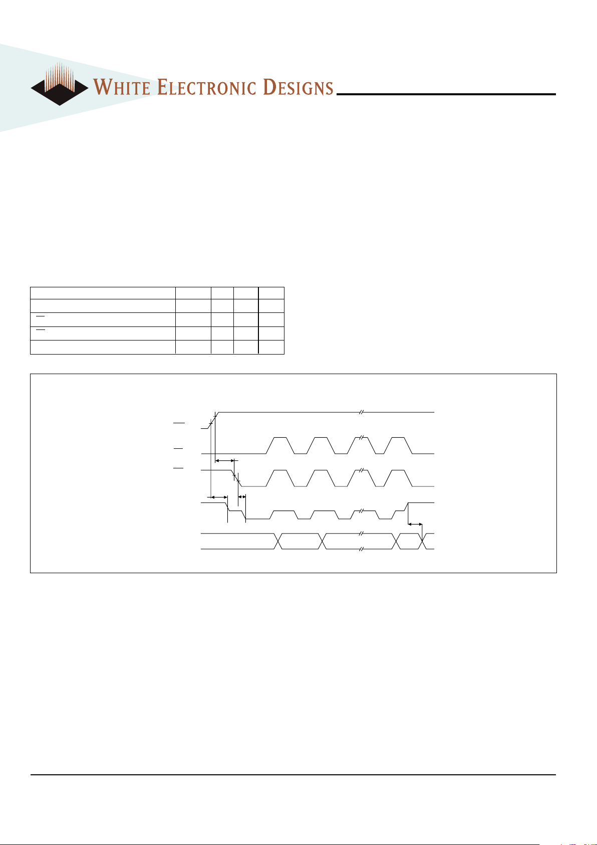
DATA POLLING
The WE128K32-XXX offers a data polling feature which allows
a faster method of writing to the device. Figure 8 shows the
timing diagram for this function. During a byte or page write
cycle, an attempted read of the last byte written will result in
the complement of the written data on D
7 (for each chip.) Once
the write cycle has been completed, true data is valid on all
outputs and the next cycle may begin. Data polling may begin
at any time during the write cycle.
DATA POLLING CHARACTERISTICS
(V
CC
= 5.0V, VSS = 0V, TA = -55°C to +125°C)
FIG. 8
DATA POLLING
WAVEFORMS
Parameter Symbol Min Max Unit
Data Hold Time tDH 10 ns
OE Hold Time tOEH 10 ns
OE To Output Valid tOE 55 ns
Write Recovery Time t
WR 0ns
WE
1-4
t
OEH
t
DH
t
OE
t
WR
HIGH Z
CS
1-4
OE
I/O
7
ADDRESS
8
White Electronic Designs Corporation • (602) 437-1520 • www.whiteedc.com
WE128K32-XXX
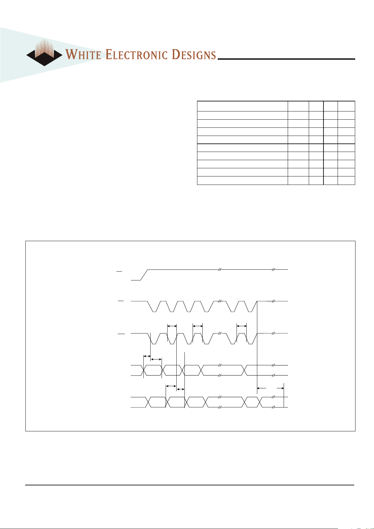
PAGE WRITE OPERATION
The WE128K32-XXX has a page write operation that allows one to
128 bytes of data to be written into the device and consecutively
loads during the internal programming period. Successive bytes
may be loaded in the same manner after the first data byte has
been loaded. An internal timer begins a time out operation at each
write cycle. If another write cycle is completed within 150µs or
less, a new time out period begins. Each write cycle restarts the
delay period. The write cycles can be continued as long as the
interval is less than the time out period.
The usual procedure is to increment the least significant
address lines from A0 through A6 at each write cycle. In this
manner a page of up to 128 bytes can be loaded in to the
EEPROM in a burst mode before beginning the relatively long
interval programming cycle.
After the 150µs time out is completed, the EEPROM begins an
internal write cycle. During this cycle the entire page of bytes
will be written at the same time. The internal programming
cycle is the same regardless of the number of bytes accessed.
PAGE WRITE CHARACTERISTICS
(V
CC
= 5.0V, VSS = 0V, TA = -55°C to +125°C)
FIG. 9
PAGE MODE
WRITE WAVEFORMS
1. Page address must remain valid for duration of write cycle.
Page Mode Write Characteristics Symbol Unit
Parameter Min Max
Write Cycle Time, TYP = 6ms tWC 10 ms
Address Set-up Time tAS 0ns
Address Hold Time (1) tAH 100 ns
Data Set-up Time tDS 100 ns
Data Hold Time tDH 10 ns
Write Pulse Width tWP 150 ns
Byte Load Cycle Time tBLC 150 µs
Write Pulse Width High t
WPH 50 ns
OE
BYTE 0 BYTE 1 BYTE 2 BYTE 3
VALID DATA
VALID
ADDRESS
t
WC
t
BLC
t
WPH
t
WP
ADDRESS
DATA
CS
WE
BYTE 127
t
DS
t
DH
t
AS
t
AH
x
x
9
White Electronic Designs Corporation • (602) 437-1520 • www.whiteedc.com
WE128K32-XXX
LOAD DATA AA
TO
ADDRESS 5555
LOAD DATA 55
TO
ADDRESS 2AAA
LOAD DATA A0
TO
ADDRESS 5555
LOAD DATA XX
TO
ANY ADDRESS
(4)
LOAD LAST BYTE
TO
LAST ADDRESS
FIG. 10
SOFTWARE DATA PROTECTION
ENABLE ALGORITHM
(1)
➞
➞
➞
➞
WRITES ENABLED
(2)
NOTES:
1. Data Format: D
7 - D0 (Hex);
Address Format: A
16 - A0 (Hex).
2. Write Protect state will be activated at end of write even if no other
data is loaded.
3. Write Protect state will be deactivated at end of write period even if
no other data is loaded.
4. 1 to 128 bytes of data may be loaded.
ENTER DATA
PROTECT STATE

10
White Electronic Designs Corporation • (602) 437-1520 • www.whiteedc.com
WE128K32-XXX
HARDWARE DATA PROTECTION
These features protect against inadvertent writes to the
WE128K32-XXX. These are included to improve reliability
during normal operation:
a) V
CC power on delay
As VCC climbs past 3.8V typical the device will wait 5msec
typical before allowing write cycles.
b) V
CC sense
While below 3.8V typical write cycles are inhibited.
c) Write inhibiting
Holding OE low and either CS or WE high inhibits write
cycles.
d) Noise filter
Pulses of <8ns (typ) on WE or CS will not initiate a write
cycle.
SOFTWARE DATA PROTECTION
A software write protection feature may be enabled or disabled
by the user. When shipped by White Microelectronics, the WE128K32-XXX has the feature disabled. Write access to the
device is unrestricted.
To enable software write protection, the user writes three
access code bytes to three special internal locations. Once
write protection has been enabled, each write to the EEPROM
must use the same three byte write sequence to permit writing.
After setting software data protection, any attempt to write to
the device without the three-byte command sequence will start
the internal write timers. No data will be written to the device,
however, for the duration of t
WC. The write protection feature
can be disabled by a six byte write sequence of specific data to
specific locations. Power transitions will not reset the
software write protection.
Each 128K byte block of the EEPROM has independent write
protection. One or more blocks may be enabled and the rest
disabled in any combination. The software write protection
guards against inadvertent writes during power transitions, or
unauthorized modification using a PROM programmer.
FIG. 11
SOFTWARE DATA PROTECTION
DISABLE ALGORITHM
(1)
➞ ➞
➞
➞
➞
➞
➞
EXIT DATA
PROTECT STATE
NOTES:
1. Data Format: D
7 - D0 (Hex);
Address Format: A
16 - A0 (Hex).
2. Write Protect state will be activated at end of write even if no other
data is loaded.
3. Write Protect state will be deactivated at end of write period even if
no other data is loaded.
4. 1 to 128 bytes of data may be loaded.
(3)
LOAD DATA AA
TO
ADDRESS 5555
LOAD DATA 55
TO
ADDRESS 2AAA
LOAD DATA 80
TO
ADDRESS 5555
LOAD DATA AA
TO
ADDRESS 5555
LOAD DATA 55
TO
ADDRESS 2AAA
LOAD DATA 20
TO
ADDRESS 5555
LOAD DATA XX
TO
ANY ADDRESS
(4)
LOAD LAST BYTE
TO
LAST ADDRESS
11
White Electronic Designs Corporation • (602) 437-1520 • www.whiteedc.com
WE128K32-XXX
PACKAGE 401: 66 PIN, PGA TYPE, CERAMIC HEX-IN-LINE PACKAGE, HIP (H)
30.1 (1.185) ± 0.38 (0.015) SQ
25.4 (1.0) TYP
15.24 (0.600) TYP
0.76 (0.030) ± 0.1 (0.005)
6.22 (0.245)
MAX
3.81 (0.150)
± 0.1 (0.005)
2.54 (0.100)
TYP
25.4 (1.0) TYP
1.27 (0.050) ± 0.1 (0.005)
1.27 (0.050) TYP DIA
0.46 (0.018) ± 0.05 (0.002) DIA
PIN 1 IDENTIFIER
SQUARE PAD
ON BOTTOM
ALL LINEAR DIMENSIONS ARE MILLIMETERS AND PARENTHETICALLY IN INCHES
PACKAGE 400: 66 PIN, PGA TYPE, CERAMIC HEX-IN-LINE PACKAGE, HIP (H1)
27.3 (1.075) ± 0.25 (0.010) SQ
PIN 1 IDENTIFIER
SQUARE PAD
ON BOTTOM
25.4 (1.0) TYP
15.24 (0.600) TYP
0.76 (0.030) ± 0.13 (0.005)
4.34 (0.171)
MAX
3.81 (0.150)
± 0.13 (0.005)
2.54 (0.100)
TYP
25.4 (1.0) TYP
1.42 (0.056) ± 0.13 (0.005)
1.27 (0.050) TYP DIA
0.46 (0.018) ± 0.05 (0.002) DIA
ALL LINEAR DIMENSIONS ARE MILLIMETERS AND PARENTHETICALLY IN INCHES

12
White Electronic Designs Corporation • (602) 437-1520 • www.whiteedc.com
WE128K32-XXX
PACKAGE 501: 68 LEAD, CERAMIC QUAD FLAT PACK, CQFP (G4)
ALL LINEAR DIMENSIONS ARE MILLIMETERS AND PARENTHETICALLY IN INCHES
0.38 (0.015)
± 0.08 (0.003)
68 PLACES
1.27 (0.050)
TYP
5.1 (0.200) MAX
39.6 (1.56) ± 0.38 (0.015) SQ
38 (1.50) TYP
4 PLACES
5.1 (0.200)
± 0.25 (0.010)
4 PLACES
12.7 (0.500)
± 0.5 (0.020)
4 PLACES
0.25 (0.010)
± 0.05 (0.002)
1.27 (0.050)
± 0.1 (0.005)
PIN 1 IDENTIFIER
Pin 1
PACKAGE 509: 68 LEAD, CERAMIC QUAD FLAT PACK, CQFP (G2T)
0.38 (0.015) ± 0.05 (0.002)
0.27 (0.011) ± 0.04 (0.002)
25.15 (0.990) ± 0.26 (0.010) SQ
1.27 (0.050) TYP
24.03 (0.946)
± 0.26 (0.010)
22.36 (0.880) ± 0.26 (0.010) SQ
20.3 (0.800) REF
4.57 (0.180) MAX
0.19 (0.007)
± 0.06 (0.002)
23.87
(0.940) REF
1.0 (0.040)
± 0.127 (0.005)
0.25 (0.010) REF
1° / 7°
R 0.25
(0.010)
DETAIL A
SEE DETAIL "A"
Pin 1
ALL LINEAR DIMENSIONS ARE MILLIMETERS AND PARENTHETICALLY IN INCHES
The White 68 lead G2T CQFP fills the same fit
and function as the JEDEC 68 lead CQFJ or 68
PLCC. But the G2T has the TCE and lead
inspection advantage of the CQFP form.
13
White Electronic Designs Corporation • (602) 437-1520 • www.whiteedc.com
WE128K32-XXX
PACKAGE 519: 68 LEAD, CERAMIC QUAD FLAT PACK, LOW PROFILE CQFP (G1U)
0.38 (0.015) ± 0.05 (0.002)
0.25 (0.010)
25.27 (0.995) ± 0.13 (0.005) SQ
1.27 (0.050)
23.88 (0.940) ± 0.25 (0.010) SQ
20.3 (0.800) REF
0.84 (0.033) REF
DETAIL A
SEE DETAIL "A"
3.56 (0.140) MAX
0.61 (0.024)
± 0.15 (0.006)
ALL LINEAR DIMENSIONS ARE MILLIMETERS AND PARENTHETICALLY IN INCHES
The White 68 lead G1U CQFP
fills the same fit and function as
the JEDEC 68 lead CQFJ or 68
PLCC. But the G1U has the TCE
and lead inspection advantage
of the CQFP form.

14
White Electronic Designs Corporation • (602) 437-1520 • www.whiteedc.com
WE128K32-XXX
LEAD FINISH:
Blank = Gold plated leads
A = Solder dip leads
DEVICE GRADE:
Q = Compliant
M = Military Screened -55°C to +125 °C
I = Industrial -40°C to +85°C
C = Commercial 0°C to +70°C
PACKAGE TYPE:
H1 = 1.075" sq. Ceramic Hex In-line Package, HIP (Package 400*)
G2T = 22.4mm Ceramic Quad Flat Pack, Low Profile CQFP (Package 509)
G1U = 22.4mm Ceramic Quad Flat Pack, Low Profile CQFP (Package 519)
G4 = 40mm Ceramic Quad Flat Pack, CQFP (Package 501)
ACCESS TIME (ns)
IMPROVEMENT MARK
N = No Connect at pins 8, 21, 28, and 39 in HIP for upgrade
P = Alternate Pin Configuration for HIP package
ORGANIZATION 128K x 32
User Configurable as 256K x 16 or 512K x 8
EEPROM
WHITE ELECTRONIC DESIGNS CORP.
ORDERING INFORMATION
W E 128K32 X - XXX X X X
I/O0-31 Data Inputs/Outputs
A0-16 Address Inputs
WE1-4 Write Enables
CS1-4 Chip Selects
OE Output Enable
VCC Power Supply
GND Ground
NC Not Connected
FIG. 12 ALTERNATE PIN CONFIGURATION FOR WE128K32NP-XH1X
PIN DESCRIPTION
BLOCK DIAGRAM
128K x 8
8
I/O
0-7
CS
1
128K x 8
8
I/O
8-15
2
128K x 8
8
I/O
16-23
3
128K x 8
8
I/O
24-31
4
A
0-16
OE
WE
CS
WE
CS
WE
CS
WE
1234
TOP VIEW
I/O
8
I/O
9
I/O
10
A
14
A
16
A
11
A
0
NC
I/O
0
I/O
1
I/O
2
WE
2
CS
2
GND
I/O
11
A
10
A
9
A
15
V
CC
CS
1
NC
I/O
3
I/O
15
I/O
14
I/O
13
I/O
12
OE
NC
WE
1
I/O
7
I/O
6
I/O
5
I/O
4
I/O
24
I/O
25
I/O
26
A
7
A
12
NC
A
13
A
8
I/O
16
I/O
17
I/O
18
V
CC
CS
4
WE
4
I/O
27
A
4
A
5
A
6
WE
3
CS
3
GND
I/O
19
I/O
31
I/O
30
I/O
29
I/O
28
A
1
A
2
A
3
I/O
23
I/O
22
I/O
21
I/O
20
11 22 33 44 55 66
1 12 23 34 45 56
15
White Electronic Designs Corporation • (602) 437-1520 • www.whiteedc.com
WE128K32-XXX
DEVICE TYPE SPEED PACKAGE SMD NO.
128K x 32 EEPROM Module 300ns 66 pin HIP (H1) 5962-94585 01H5X
128K x 32 EEPROM Module 250ns 66 pin HIP (H1) 5962-94585 02H5X
128K x 32 EEPROM Module 200ns 66 pin HIP (H1) 5962-94585 03H5X
128K x 32 EEPROM Module 150ns 66 pin HIP (H1) 5962-94585 04H5X
128K x 32 EEPROM Module 140ns 66 pin HIP (H1) 5962-94585 05H5X
128K x 32 EEPROM Module 300ns 66 pin HIP (H1, P type pinout) 5962-94585 01H6X
128K x 32 EEPROM Module 250ns 66 pin HIP (H1, P type pinout) 5962-94585 02H6X
128K x 32 EEPROM Module 200ns 66 pin HIP (H1, P type pinout) 5962-94585 03H6X
128K x 32 EEPROM Module 150ns 66 pin HIP (H1, P type pinout) 5962-94585 04H6X
128K x 32 EEPROM Module 140ns 66 pin HIP (H1, P type pinout) 5962-94585 05H6X
128K x 32 EEPROM Module 300ns 68 lead CQFP/J (G2T) 5962-94585 01HMX
128K x 32 EEPROM Module 250ns 68 lead CQFP/J (G2T) 5962-94585 02HMX
128K x 32 EEPROM Module 200ns 68 lead CQFP/J (G2T) 5962-94585 03HMX
128K x 32 EEPROM Module 150ns 68 lead CQFP/J (G2T) 5962-94585 04HMX
128K x 32 EEPROM Module 140ns 68 lead CQFP/J (G2T) 5962-94585 05HMX
128K x 32 EEPROM Module 300ns 68 lead CQFP (G4) 5962-94585 01HNX
128K x 32 EEPROM Module 250ns 68 lead CQFP (G4) 5962-94585 02HNX
128K x 32 EEPROM Module 200ns 68 lead CQFP (G4) 5962-94585 03HNX
128K x 32 EEPROM Module 150ns 68 lead CQFP (G4) 5962-94585 04HNX
128K x 32 EEPROM Module 140ns 68 lead CQFP (G4) 5962-94585 05HNX
128K x 32 EEPROM Module 300ns 68 lead CQFP (G1U) 5962-94585 01H9X
128K x 32 EEPROM Module 250ns 68 lead CQFP (G1U) 5962-94585 02H9X
128K x 32 EEPROM Module 200ns 68 lead CQFP (G1U) 5962-94585 03H9X
128K x 32 EEPROM Module 150ns 68 lead CQFP (G1U) 5962-94585 04H9X
128K x 32 EEPROM Module 140ns 68 lead CQFP (G1U) 5962-94585 05H9X
 Loading...