

White Electronic Designs
A
1Mx8 STATIC RAM CMOS, MODULE
EDI8F81026C
FEATURES
1Mx8 bit CMOS Static RAM
• Access Times 20 through 35ns
• TTL Compatible Inputs and Outputs
• Fully Static, No Clocks
High Density Packaging
• JEDEC Aproved, Revolutionary Pinout
• 36 Pin DIP, No. 179
Single +5V (±10%) Supply Operation
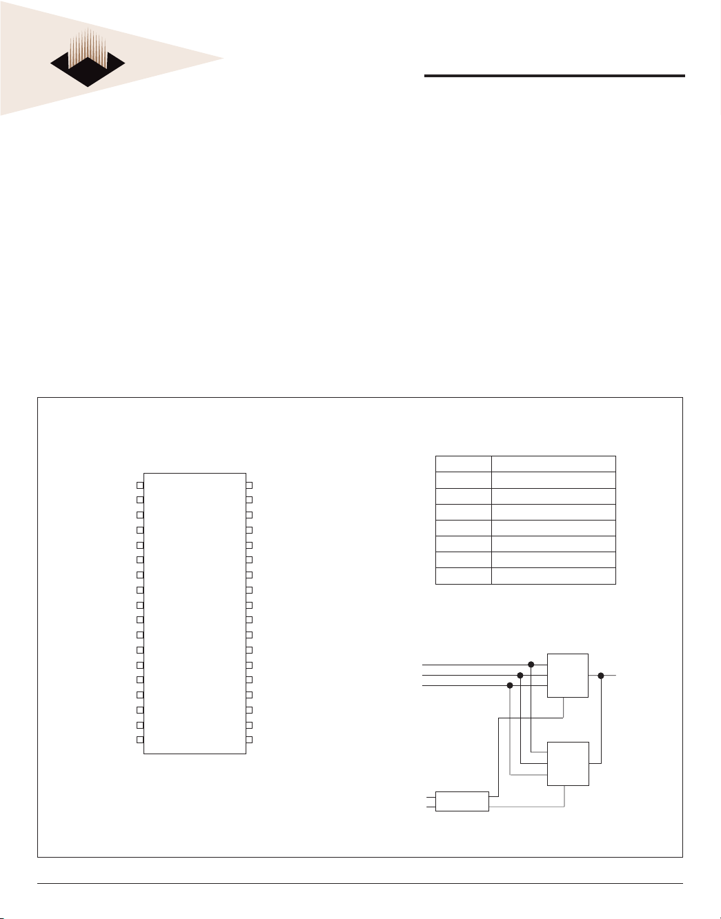
Pin Confi guration
1
A0
2
A1
3
A2
4
A3
5
A4
6
E#
7
DQ0
8
DQ1
9
V
CC
10
V
SS
11
DQ2
12
DQ3
13
W#
14
A5
15
A6
16
A7
17
A8
18
A9
36
35
34
33
32
31
30
29
28
27
26
25
24
23
22
21
20
19
NC
A19
A18
A17
A16
G#
DQ7
DQ6
V
SS
V
CC
DQ5
DQ4
A15
A14
A13
A12
A11
A10
DESCRIPTION
The EDI8F81026C is an 8Mb CMOS Static RAM based
on two 512Kx8 Static RAMs mounted on a multi-layered
epoxy laminate (FR4) substrate.
The EDI8F81026C is packaged in a 36 pin DIP and features
the JEDEC approved, revolutionary pinout.
All inputs and outputs are TTL compatible and operate from
a single 5V supply.
Fully asynchronous, the EDI8F81026C requires no clocks
or refreshing for operation.
Pin Description
A0-A19 Address Inputs
E# Chip Enable
W# Write Enable
G# Output Enable
DQ0-DQ7 Common Data Input/Output
0-A18
W#
G#
V
CC
V
SS
NC No Connection
Power (+5V±10%)
Ground
Block Diagram
512k
x 8
512k
x 8
DQ0-DQ7
July 2004
Rev. 0
A19
DECODER
E#
1
White Electronic Designs Corporation • (602) 437-1520 • www.wedc.com
White Electronic Designs
EDI8F81026C
ABSOLUTE MAXIMUM RATINGS*
Voltage on any pin relative to V
Operating Temperature T
SS
(Ambient)
A
Commercial 0°C to +70°C
Industrial -40°C to +85°C
Storage Temperature -55°C to +125°C
Power Dissipation 2.0 Watt
Output Current 20 mA
* Stress greater than those listed under "Absolute Maximum Ratings" may cause
permanent damage to the device. This is a stress rating only and functional
operation of the device at these or any other conditions greater than those indicated
in the operational sections of this specifi cation is not implied. Exposure to absolute
maximum rating conditions for extended periods may affect reliability.
-0.5V to 7.0V
TRUTH TABLE
G# E# W# Mode Output Power
X H X Standby High Z I
H L H Output Deselect High Z ICC1
L L H Read D
X L L Write D
OUT
IN
CC
2, ICC3
ICC1
ICC1
RECOMMENDED DC OPERATING CONDITIONS
Parameter Sym Min Typ Max Units
Supply Voltage VCC 4.5 5.0 5.5 V
Supply Voltage V
Input High Voltage V
Input Low Voltage V
SS
000V
2.2 — 6.0 V
IH
-0.3 — 0.8 V
IL
AC TEST CONDITIONS
Input Pulse Levels VSS to 3.0V
Input Rise and Fall Times 5ns
Input and Output Timing Levels 1.5V
Output Load 1TTL, CL =35pF
(Note: For t
EHQZ
, t
and t
WLQZ
, CL=5pF)
GHQZ
CAPACITANCE
(f=1.0MHz, VIN=VCC or VSS)
Parameter Sym Max Unit
Address Lines CI 12 pF
Data Lines CD/Q 43 pF
Chip Enable Line CC 10 pF
Write and Output Enable Lines CW 32 pF
These parameters are sampled, not 100% tested.
DC ELECTRICAL CHARACTERISTICS
Parameter Sym Conditions Min Typ* Max Units
Operating Power Supply Current I
Standby (TTL) Power Supply Current I
Full Standby Power Supply Current (CMOS) I
Input Leakage Current I
Output Leakage Current I
Output High Voltage V
Output Low Voltage V
*Typical: TA = 25°C, VCC = 5.0V
July 2004
Rev. 0
W#, E# = VIL, I
CC1
E > VIH, VIN < V
CC2
E > VCC-0.2V, VIN > VCC-0.2V or VIN< 0.2V — 20 12 mA
CC3
VIN = 0V to VCC — — ±10 µA
LI
V I/O = 0V to V
LO
OHIOH
OLIOL
=-4.0mA 2.4 — — V
= 8.0mA — — 0.4 V
= 0mA, Min Cycle — 212 120 mA
I/O
IL, VIN
CC
2
> V
IH
White Electronic Designs Corporation • (602) 437-1520 • www.wedc.com
—3550mA
— — ±10 µA

White Electronic Designs
EDI8F81026C
AC CHARACTERISTICS READ CYCLE
Parameter Symbol 20ns 25ns 35ns Units
JEDEC Alt. Min Max Min Max Min Max
Read Cycle Time t
Address Access Time t
Chip Enable Access Time t
Chip Enable to Output in Low Z (1) t
Chip Disable to Output in High Z (1) t
Output Hold from Address Change t
Output Enable to Output Valid t
Output Enable to Output in Low Z (1) t
Output Disable to Output in High Z(1) t
Note 1: Parameter guaranteed, but not tested
AVAV
AVQ V
ELQV
ELQX
EHQZ
AVQ X
GLQV
GLQX
GHQZtOHZ
t
t
t
ACS
t
CLZ
t
CHZ
t
t
t
LOZ
20 25 35 ns
RC
AA
20 25 35 ns
20 25 35 ns
333ns
10 12 15 ns
OH
OE
333ns
81012ns
333ns
81012ns
FIGURE 2 – READ CYCLE 1 - W# HIGH, G#, E# LOW
t
AVAV
A
ADDRESS 1
ADDRESS 2
t
AVQ V
Q
tAVQ X
DATA 1
DATA 2
FIGURE 3 – READ CYCLE 2 - W# HIGH
AVAV
t
A
E#
G#
Q
tELQX
tAVQ V
tELQV
tGLQV
tGLQX
tEHQZ
tGHQZ
July 2004
Rev. 0
3
White Electronic Designs Corporation • (602) 437-1520 • www.wedc.com

White Electronic Designs
EDI8F81026C
AC CHARACTERISTICS WRITE CYCLE
Parameter Symbol 20ns 25ns 35ns Units
JEDEC Alt. Min Max Min Max Min Max
Write Cycle Time t
Chip Enable to End of Write t
Address Setup Time t
Address Valid to End of Write t
Write Pulse Width t
Write Recovery Time t
Data Hold Time t
Write to Output in High Z (1) t
Data to Write Time t
Output Active from End of Write (1) t
Note 1: Parameter guaranteed, but not tested.
AVAV
ELWH
t
ELEH
AVW L
t
AVE L
AVW H
t
AVE H
WLWH
t
WLEH
WHAX
t
EHAX
WHDX
t
EHDX
WLQZ
DVWH
t
DVEH
WHQX
t
WC
t
CW
t
CW
t
AS
t
AS
t
AW
t
AW
t
WP
t
WP
t
WR
t
WR
t
DH
t
DH
t
WHZ
t
DW
t
DW
t
WLZ
20 25 35 ns
15
15
0
0
15
15
15
15
0
0
0
0
20
20
0
0
15
15
20
20
0
0
0
0
30
30
0
0
20
20
25
25
0
0
0
0
08012015ns
12
12
15
15
20
20
333ns
ns
ns
ns
ns
ns
ns
ns
ns
ns
ns
ns
ns
ns
ns
E#
W#
FIGURE 4 – WRITE CYCLE 1 - W# CONTROLLED
AVAV
t
A
tELWH
tAVW H
tWLWH
tAVW L
tDVWH
D
DATA VALID
tWLQZ
Q
HIGH Z
tWHAX
tWHDX
tWHQX
July 2004
Rev. 0
4
White Electronic Designs Corporation • (602) 437-1520 • www.wedc.com

White Electronic Designs
FIGURE 5 – WRITE CYCLE 2 E# CONTROLLED
t
AVAV
EDI8F81026C
A
E#
W#
t
AVEL
tAVEH tEHAX
D
Q
HIGH Z
ORDERING INFORMATION
Standard Power Speed (ns) Package No. Height*
EDI8F81026C20M6C 20 179 7.37 (0.290")
EDI8F81026C85M6C 25 179 7.37 (0.290")
EDI8F81026C35M6C 35 179
Note: To order an Industrial grade product substitute the letter C in the Suffi x with the letter I,
eg. EDI8F81026C20M6C becomes EDI8F81026C20M6I.
PACKAGE DESCRIPTION
Package No. 179: 36 Pin Dual-in-line Package
tELEH
tWLEH
tEHDXtDVEH
DATA VALID
7.37 (0.290")
July 2004
Rev. 0
3.81
(0.150)
REF.
55.50
(2.185) MAX.
15.88
(0.625)
MAX.
P1
7.34
(0.290)
MAX.
2.54 (0.100) TYP.
17 X 2.54 (0.100)
43.18 (1.700) REF.
* ALL DIMENSIONS ARE IN MILLIMETERS AND (INCHES).
5
4.45 (0.175)
3.18 (0.125)
White Electronic Designs Corporation • (602) 437-1520 • www.wedc.com
15.75 (0.620)
14.99 (0.590)

White Electronic Designs
EDI8F81026C
Document Title
1M X 8 SRAM Module
Revision History
Rev # History Release Date Status
Rev 0 0.1 Updated datasheet format
0.2 Added package height
0.3 Added metric measurements
0.4 Added new document title page
7-2004 Final
July 2004
Rev. 0
6
White Electronic Designs Corporation • (602) 437-1520 • www.wedc.com
 Loading...