

Page 1
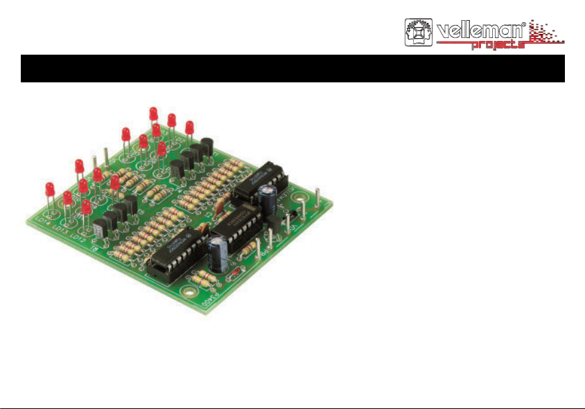
DUAL ELECTRONIC DICE
K3400
ILLUSTRATED ASSEMBLY MANUAL H3400IP-1
C
h
e
a
t
i
n
g
i
s
no
l
o
n
g
e
r
pos
s
i
b
l
e
!
Page 2

VELLEMAN NV
Legen Heirweg 33
9890 Gavere
Belgium Europe
www.velleman.be
www.velleman-kit.com
Page 3

3
Features:
Two independent dice.
Use a single or both dice at the same time.
Display auto shut-off saves battery power.
Low power consumption.
Specifications:
Power supply : 8-12VDC or 6VAC.
Idle power consumption : 1mA.
Power consumption both dice on : 60mA.
PCB dimensions: 76 x 70mm (3.0" x 2.8")
Features & Specifications
Page 4
4
Assembly hints
1. Assembly (Skipping this can lead to troubles ! )
Ok, so we have your attention. These hints will help you to make this project successful. Read them carefully.
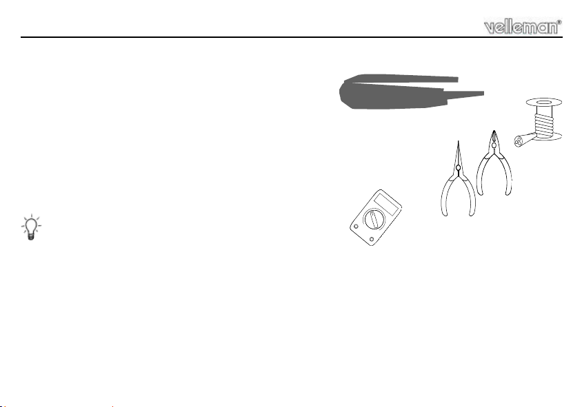
1.1 Make sure you have the right tools:
A good quality soldering iron (25-40W) with a small tip.
Wipe it often on a wet sponge or cloth, to keep it clean; then apply solder to the tip, to give it a wet look. This is called ‘thinning’ and will
protect the tip, and enables you to make good connections. W hen solder rolls off the tip, it needs cleaning.
Thin raisin-core solder. Do not use any flux or grease.
A diagonal cutter to trim excess wires. To avoid injury when cutting excess leads, hold the lead so they
cannot fly towards the eyes.
Needle nose pliers, for bending leads, or to hold components in place.
Small blade and Phillips screwdrivers. A basic range is fine.
For some projects, a basic multi-meter is required, or might be handy
1.2 Assembly Hints :
Make sure the skill level matches your experience, to avoid disappointments.
Follow the instructions carefully. Read and understand the entire step before you perform each operation.
Perform the assembly in the correct order as stated in this manual
Position all parts on the PCB (Printed Circuit Board) as shown on the drawings.
Values on the circuit diagram are subject to changes.
Values in this assembly guide are correct*
Use the check-boxes to mark your progress.
Please read the included information on safety and customer service
* Typographical inaccuracies excluded. Always look for possible last minute manual updates, indicated as ‘NOTE’ on a separate leaflet.
0
.
0
0
0
Page 5
5
Assembly hints
1.3 Soldering Hints :
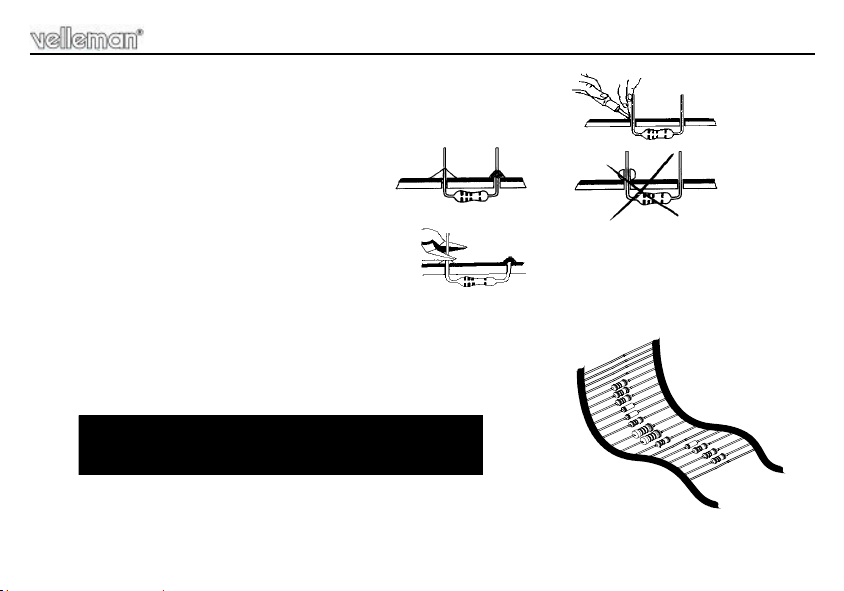
1- Mount the component against the PCB surface and carefully solder the leads
2- Make sure the solder joints are cone-shaped and shiny
3- Trim excess leads as close as possible to the solder joint
REMOVE THEM FROM THE TAPE ONE AT A TIME !
AXIAL COMPONENTS ARE TAPED IN THE
CORRECT MOUNTING SEQUENCE !
Page 6
6
Construction
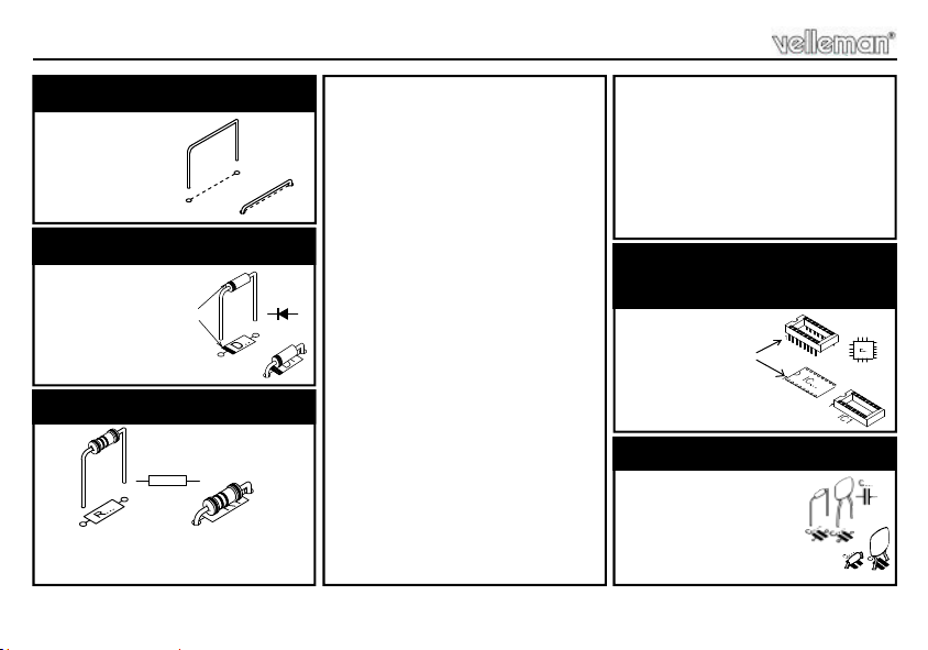
D1 : 1N4148
D2 : 1N4007
2. Diodes. Watch the polarity!
D...
CATHODE
R1 : 4K7 (4 - 7 - 2 - B)
R2 : 470K (4 - 7 - 4 - B)
3. 1/4W Resistors
R...
J : 2x
1. Jumpers
R30 : 680 (6 - 8 - 1 - B)
R31 : 680 (6 - 8 - 1 - B)
R32 : 470 (4 - 7 - 1 - B)
R33 : 470 (4 - 7 - 1 - B)
R34 : 470 (4 - 7 - 1 - B)
R35 : 470 (4 - 7 - 1 - B)
R36 : 470 (4 - 7 - 1 - B)
R37 : 470 (4 - 7 - 1 - B)
R3 : 47K (4 - 7 - 3 - B)
R4 : 47K (4 - 7 - 3 - B)
R5 : 47K (4 - 7 - 3 - B)
R6 : 47K (4 - 7 - 3 - B)
R7 : 47K (4 - 7 - 3 - B)
R8 : 47K (4 - 7 - 3 - B)
R9 : 47K (4 - 7 - 3 - B)
R10 : 47K (4 - 7 - 3 - B)
R11 : 47K (4 - 7 - 3 - B)
R12 : 47K (4 - 7 - 3 - B)
R13 : 47K (4 - 7 - 3 - B)
R14 : 47K (4 - 7 - 3 - B)
R15 : 47K (4 - 7 - 3 - B)
R16 : 47K (4 - 7 - 3 - B)
R17 : 47K (4 - 7 - 3 - B)
R18 : 47K (4 - 7 - 3 - B)
R19 : 47K (4 - 7 - 3 - B)
R20 : 47K (4 - 7 - 3 - B)
R21 : 47K (4 - 7 - 3 - B)
R22 : 47K (4 - 7 - 3 - B)
R23 : 47K (4 - 7 - 3 - B)
R24 : 47K (4 - 7 - 3 - B)
R25 : 47K (4 - 7 - 3 - B)
R26 : 47K (4 - 7 - 3 - B)
R27 : 47K (4 - 7 - 3 - B)
R28 : 47K (4 - 7 - 3 - B)
R29 : 47K (4 - 7 - 3 - B)
IC1 : 16p
IC2 : 16P
IC3 : 14P
PIN1
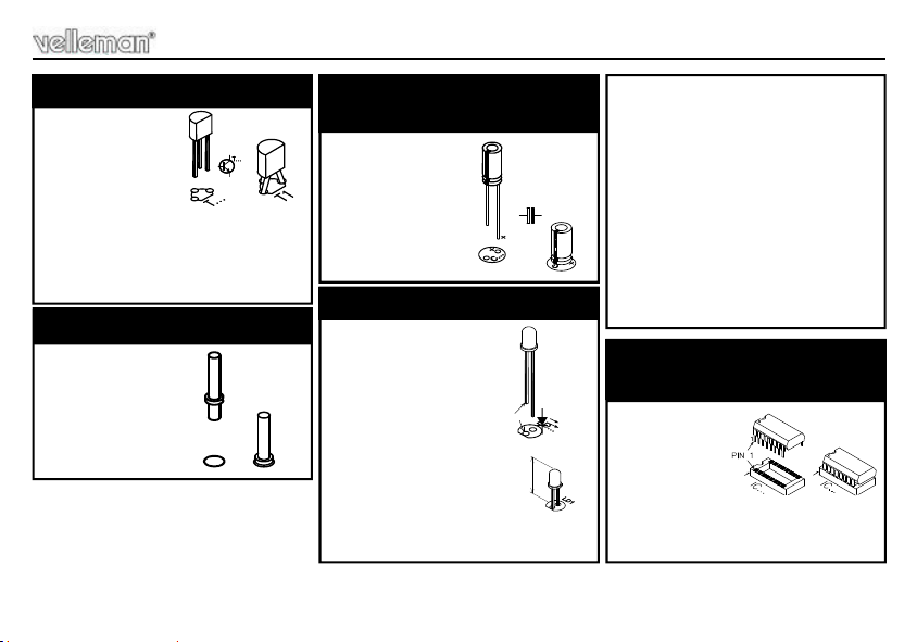
4. IC sockets. Pay attention
to the position of the notch!
C1 : 390pF (391)
C2 : 470pF (471)
5. Capacitors
Page 7
7
Construction
C3 : 100µF
C4 : 100µF
C...
+
VD
PB (2x)
VD1
VD2
7. PCB pins
T1 : BC547B
T2 : BC547B
T3 : BC547B
T4 : BC547B
T5 : BC547B
T6 : BC547B
T7 : BC547B
T8 : BC547B
T9 : BC557B
6. Transistors
LD1 : 3mm red
LD2 : 3mm red
LD3 : 3mm red
LD4 : 3mm red
LD5 : 3mm red
LD6 : 3mm red
LD7 : 3mm red
LD8 : 3mm red
LD9 : 3mm red
LD10 : 3mm red
LD11 : 3mm red
LD12 : 3mm red
9. LED’s. Watch the polarity!
COLOR= 2...5
CATHODE
15mm
LD...
8. Electrolytic capacitors.
Watch the polarity!
LD13 : 3mm red
LD14 : 3mm red
Pay attention to the polarity!
As to the height of the leds,
take into account the housing
that will be used.
Mount them high enough
anyway to make them overtop
all other components. The leds
must all stand upright and be
at the same height.
IC1 : 4022
IC2 : 4022
IC3 : 4093
Pay attention to the position
of the notch!
10. IC’s. Pay attention to the
notch !
Page 8

8
Connection & test
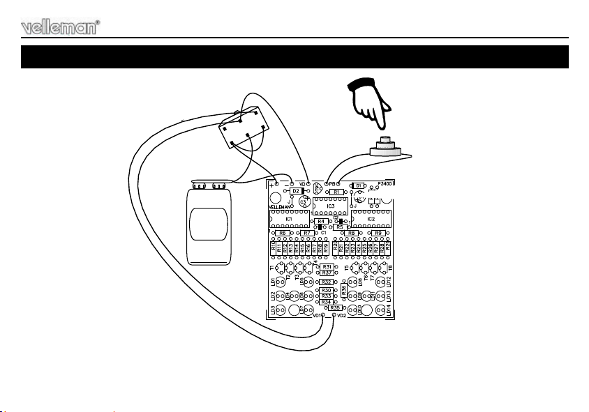
The push button (single pole normally open contact) has to be connected to the points PB.
Display selection is done by connecting VD1 respectively VD2 to VD.
You can make these connections permanent, or use a bipolar three position slide switch as shown in the
connections diagram. In this case the slide switch functions as selector and on/off- switch at the same time.
The power supply has to be connected to the points + and -. At choice you can use a 9V battery, a 8 to 12V
power supply, or a 6V transformer.
For testing you select both displays.
Push the button. As long as you push, the leds all burn feebly. This is because the dice are 'rolling'. Cheating
is out of the question, thanks to the very high and different speeds of both dice.
The result appears as soon as you release the button.
After about half a minute displays are switched off, so that current consumption is reduced to less than
1mA.
11. Connection & test
Page 9
9
9V
Battery
+
-
O
F
F
USE A SLIDE SWITCH (ON OFF ON)
12. Connection example
Connection example
Page 10
10
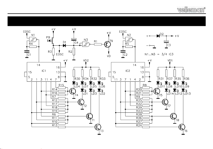
13. Schematic diagram.
Schematic diagram
Page 11

11
PCB
14. PCB
Page 12

5 410329 324612
Modifications and typographical errors reserved
© Velleman nv.
H3400IP’1 - 2014 (rev.1)
Follow Velleman R&D at Twitter
@velleman_RnD
 Loading...