

Page 1

PRODUCT MANUAL
PC SN730 NVMe™ SSD
For Generic OEM
00-01-WW-04-00047
Page 2

Revision History
Revision Date Description Reference
1.0 November 22, 2019 Initial release.
Western Digital Technologies, Inc. or its affiliates' (collectively “Western Digital”) general policy does
not recommend the use of its products in life support applications where in a failure or malfunction of
the product may directly threaten life or injury. Per Western Digital Terms and Conditions of Sale, the
user of Western Digital products in life support applications assumes all risk of such use and
indemnifies Western Digital against all damages.
This document is for information use only and is subject to change without prior notice. Western
Digital assumes no responsibility for any errors that may appear in this document, nor for incidental or
consequential damages resulting from the furnishing, performance or use of this material.
Absent a written agreement signed by Western Digital or its authorized representative to the
contrary, Western Digital explicitly disclaims any express and implied warranties and indemnities of
any kind that may, or could, be associated with this document and related material, and any user of
this document or related material agrees to such disclaimer as a precondition to receipt and usage
hereof.
Each user of this document or any product referred to herein expressly waives all guaranties and
warranties of any kind associated with this document any related materials or such product, whether
expressed or implied, including without limitation, any implied warranty of merchantability or fitness
for a particular purpose or non-infringement. Each user of this document or any product referred to
herein also expressly agrees Western Digital shall not be liable for any incidental, punitive, indirect,
special, or consequential damages, including without limitation physical injury or death, property
damage, lost data, loss of profits or costs of procurement of substitute goods, technology, or
services, arising out of or related to this document, any related materials or any product referred to
herein, regardless of whether such damages are based on tort, warranty, contract, or any other legal
theory, even if advised of the possibility of such damages.
This document and its contents, including diagrams, schematics, methodology, work product, and
intellectual property rights described in, associated with, or implied by this document, are the sole
and exclusive property of Western Digital. No intellectual property license, express or implied, is
granted by Western Digital associated with the document recipient's receipt, access and/or use of
this document or the products referred to herein; Western Digital retains all rights hereto.
Western Digital, the Western Digital logo, and nCache are registered trademarks or trademarks of
Western Digital Corporation or its affiliates in the US and/or other countries. The NVMe word mark is
a trademark of NVM Express, Inc. All other marks are the property of their respective owners. Product
specifications subject to change without notice. Pictures shown may vary from actual products. Not
all products are available in all regions of the world.
© 2019 Western Digital Corporation or its affiliates. All rights reserved.
- 2 - 00-01-WW-04-00047
Page 3

Table of Contents
TABLE OF CONTENTS
1. PREFACE........................................................................................................................... 7
1.1 Typographical Conventions ............................................................................................................7
1.2 Glossary of Abbreviations and Acronyms......................................................................................7
2. INTRODUCTION ................................................................................................................. 8
2.1 General Description ........................................................................................................................ 8
2.2 Key Features and Specification.......................................................................................................9
2.3 Functional Description ...................................................................................................................10
2.4 Advanced Flash Management .......................................................................................................10
2.4.1 Defect and Error Management ............................................................................................ 10
2.4.2 Wear Leveling ...................................................................................................................... 10
2.4.3 Bad Block Management....................................................................................................... 10
2.4.4 Background Garbage Collection ........................................................................................10
2.4.5 SLC Cache - nCache 3.0 .......................................................................................................11
2.4.6 Error Correction Layers ........................................................................................................11
3. GENERAL PRODUCT SPECIFICATIONS .................................................................................12
3.1 Interface .......................................................................................................................................... 12
3.2 Hardware Configuration ................................................................................................................ 12
3.3 Capacity .......................................................................................................................................... 12
4. PERFORMANCE .................................................................................................................13
OWER CHARACTERISTICS................................................................................................14
5. P
5.1 Supply Voltage ............................................................................................................................... 14
5.2 Average Active-Power Consumption........................................................................................... 14
5.3 Operating Power Consumption – Average Maximum ................................................................ 14
5.4 Peak Power and In-Rush Current .................................................................................................. 15
5.5 NVMe Power Management ............................................................................................................ 15
5.6 Graceful Power-off Requirements ................................................................................................ 16
6. THERMAL THROTTLING .....................................................................................................17
6.1 Self-Thermal Throttling .................................................................................................................. 17
6.2 Denial of Service............................................................................................................................. 17
7. ENDURANCE.....................................................................................................................18
ECURITY ........................................................................................................................19
8. S
8.1 Password Lock Through TCG Pyrite 2.0 ...................................................................................... 19
8.2 Secure Erase .................................................................................................................................. 20
8.3 Security of Read-Only Mode ........................................................................................................ 20
8.4 Secure Field Firmware Update (FFU)............................................................................................ 21
8.5 Secure Boot .................................................................................................................................... 21
8.6 Secure RMA..................................................................................................................................... 21
9. PHYSICAL SPECIFICATIONS...............................................................................................22
- 3 - 00-01-WW-04-00047
Page 4

Table of Contents
9.1 M.2 2280 Form Factor ................................................................................................................... 22
10. ENVIRONMENTAL SPECIFICATIONS .................................................................................... 23
10.1 Temperature ...................................................................................................................................23
10.2 Humidity..........................................................................................................................................23
10.3 Vibration..........................................................................................................................................23
10.4 Shock ...............................................................................................................................................23
10.5 Altitude............................................................................................................................................24
10.6 Electrostatic Discharge (ESD) .......................................................................................................24
10.7 Acoustics .........................................................................................................................................24
10.8 Chemical Restrictions ....................................................................................................................24
10.9 Regulatory Agency Approvals and Declarations ....................................................................... 25
11. RELIABILITY CHARACTERISTICS......................................................................................... 27
11.1 Error Rate ........................................................................................................................................27
11.2 Mean Time to Failure (MTTF) .........................................................................................................27
12. WINDOWS DEVICE CERTIFICATIONS................................................................................. 28
12.1 HCK Certification........................................................................................................................... 28
12.2 HLK Certification ........................................................................................................................... 28
13. INTERFACE...................................................................................................................... 29
13.1 Supported Standards.................................................................................................................... 29
13.2 Pin Assignments - M.2 2280, M Key ............................................................................................. 29
14. SUPPORTED NVME COMMANDS AND FEATURES ................................................................30
14.1 NVMe Command Set..................................................................................................................... 30
14.2 Identify Controller Response ........................................................................................................ 31
14.3 Log Pages....................................................................................................................................... 38
14.3.1 SMART/Health Information (Log Identifier 02h)...............................................................39
14.3.2 Program/Erase SMART Counters (Log Identifier CDh) ...................................................39
15. ORDERING INFORMATION.................................................................................................40
ONTACT INFORMATION...................................................................................................41
16. C
- 4 - 00-01-WW-04-00047
Page 5

List of Figures
LIST OF FIGURES
Figure 2-1 Western Digital PC SN730 NVMe SSD Tiered Caching Technology .......................................11
Figure 9-1 Top and side view of the PC SN730 NVMe SSD ...................................................................... 22
- 5 - 00-01-WW-04-00047
Page 6

List of Tables
LIST OF TABLES
Table 1-1 Typographical Conventions...........................................................................................................7
Table 1-2 Glossary of Abbreviations and Acronyms ....................................................................................7
Table 2-1 Key Features and Specifications for Western Digital PC SN730 NVMe SSD.............................9
Table 3-1 PC SN730 NVMe SSD Hardware Configuration.......................................................................... 12
Table 3-2 Western Digital CL SN730 NVMe SSD Capacity Specification ................................................ 12
Table 4-1 Western Digital PC SN730 NVMe SSD M.2 2280 Performance................................................. 13
Table 5-1 Western Digital PC SN730 NVMe SSD Supply Voltage............................................................. 14
Table 5-2 Western Digital PC SN730 NVMe SSD Average Active-Power Consumption........................ 14
Table 5-3 Western Digital PC SN730 NVMe SSD Average Max Power Consumption ............................ 14
Table 5-4 Western Digital PC SN730 NVMe SSD Peak Power and In-Rush Current ............................... 15
Table 5-5 PC SN730 NVMe SSD Power Consumption and Performance Per NVMe Power State ......... 15
Table 6-1 Western Digital PC SN730 NVMe SSD Performance Under Thermal Throttling ..................... 17
Table 7-1 Western Digital PC SN730 NVMe SSD Endurance ..................................................................... 18
Table 8-1 Western Digital PC SN730 NVMe SSD Format NVM Modes and Results................................ 20
Table 9-1 PC SN730 NVMe SSD M.2 2280 Form Factor Mechanical Specifications................................ 22
Table 10-1 Western Digital PC SN730 NVMe SSD Temperature Specification ........................................23
Table 10-2 Western Digital PC SN730 NVMe SSD Humidity Specification ..............................................23
Table 10-3 Western Digital PC SN730 NVMe SSD Vibration Specification..............................................23
Table 10-4 Western Digital PC SN730 NVMe SSD Shock Specification ...................................................23
Table 10-5 Western Digital PC SN730 NVMe SSD Altitude Specification................................................24
Table 10-6 Western Digital PC SN730 NVMe SSD ESD Specification.......................................................24
Table 11-1 Western Digital PC SN730 NVMe SSD MTTF .............................................................................27
Table 13-1 M.2 Pin Assignments .................................................................................................................. 29
Table 14-1 Admin Commands...................................................................................................................... 30
Table 14-2 NVM Commands........................................................................................................................ 30
Table 14-3 Set Features/Get Features........................................................................................................ 31
Table 14-4 Controller Capabilities and Features........................................................................................ 31
Table 14-5 Admin Command Set Attributes and Optional Controller Capabilities ................................32
Table 14-6 NVM Command Set Attributes..................................................................................................34
Table 14-7 Power State Descriptors............................................................................................................35
Table 14-8 Vendor Specific (VS) ................................................................................................................. 38
Table 14-9 PC SN730 NVMe SSD Log Pages .............................................................................................. 38
Table 14-10 Western Digital PC SN730 NVMe SSD SMART/Health Information .....................................39
Table 14-11 Program/Erase SMART Counters (Log Identifier CDh) ..........................................................39
Table 15-1 PC SN730 NVMe SSD Ordering Information ............................................................................ 40
Table 15-2 PC SN730 NVMe SSD Products SKUs....................................................................................... 40
- 6 - 00-01-WW-04-00047
Page 7

1.0 PREFACE
1.1 Typographical Conventions
This document uses the typographical conventions listed and shown in Table 1-1.
Table 1-1. Typographical Conventions
Preface
Convention Usage Examples
Note: Important additional information or fur-
ther explanation of a topic.
Bold A command or system input that you
type, or text or a button displayed on a
screen.
Italics Italic font indicates any of the following:
A term with a specific meaning in the
context of this document.
Emphasis on specific information.
Reference to another document.
Blue Text References hyperlinks. For more details, visit
Note: A weekly backup is recommended.
Click HELP for details on disaster recovery.
Detailed information on disas-
ter recovery methods is available in Administrator Guide.
www.westerndigital.com
1.2 Glossary of Abbreviations and Acronyms
This section shows the glossary of abbreviations and acronyms used in this
document.
Table 1-2. Glossary of Abbreviations and Acronyms
Abbreviation/Acronyms Definition
AES Advanced Encryption Standard
APST Autonomous Power State Transitions
ASPM Active State Power Management
ECC Error Correction Code
EDC Error Detection Code
ESD Electrostatic Discharge
FFU Field Firmware Update
FW Firmware
HCTM Host Control Thermal Management
LBA Logical Block Addressing
LDPC Low-Density Parity Check
MLC Multi Level Cell
MTTF Mean Time to Failure
NVMe Non-Volatile Memory Express
PCIe Peripheral Component Interconnect Express
RTD3 Runtime D3
SSC Security Subsystem Class
SD Storage Device
SED Self-Encrypting Drive
SLC Single Level Cell
SSD Solid State Drive
TBW Terabytes Written
TCG Trusted Computing Group
TLC Triple Level Cell
- 7 - 00-01-WW-04-00047
Page 8

2.0 INTRODUCTION
This manual describes the functional, mechanical, and interface specifications of the Western
Digital® PC SN730 NVMe™ SSD.
2.1 General Description
The Western Digital PC SN730 NVMe SSD was designed to deliver high performance
and ultra-low power standby mode for Notebooks, Desktops and Ultrathin NVMe
platforms.
The proven Western Digital in-house architecture is optimized for the client SSD, both
corporate and commercial, platforms needs. Among other features, the PC SN730
NVME SSD supports the nCache™ 3.0 for SLC management, the power optimized 3
Gear LDPC Hardware Engine, BICS4 multi-pages XOR protection and a full ECC datapath protection.
The nCache 3.0 is the 3rd Generation of Western Digital Caching architecture,
introducing both Reads and Writes speed enhancements. It supports an enhanced
evacuation policy, allowing the SLC to be empty faster, and as well as direct-TLC
access for faster (write) direct access.
The PC SN730 NVME SSD is optimized for the demanding power and thermal
management requirements of low power hosts. It features an NVMe Low-Power state,
NVMe Power Management, NVMe HCTM (Host Control Thermal Management), NVMe
APST (Autonomous Power State Transitions) and NVMe ASPM (Active State Power
Management). In addition, PC SN730 NVME SSD includes a self-thermal throttling
mechanism as the last level of thermal protection
Introduction
The PC SN730 NVME SSD is available in M.2 2280 single sided form factor, with
1
capacities of 256, 512 and 1024 gigabytes (GB)
.
1
1 gigabyte (GB) = 1 billion bytes. Actual capacity may be less due to operating environment.
- 8 - 00-01-WW-04-00047
Page 9

Introduction
2.2 Key Features and Specification
Table 2-1. Key Features and Specifications for Western Digital PC SN730 NVMe SSD
Uncorrectable bit error rate (UBER)
Non-Operating Temperature and Storage
Operating and Non-Operating Shock 1500G, 0.5ms, half sine, 3 pulses x 6 surfaces
1
Logical capacity of the drive conforms to the IDEMA HDD Specification. See www.idema.org for details. A portion of the
drive capacity is not available for data storage. 1 gigabyte (GB) = 1 billion bytes.
2
Performance is measured by CrystalDiskMark 6.0.2 using 1GB LBA range. Windows 10 using Microsoft driver build 17134.112,
Secondary drive FOB. ASUS Z270-A platform with Intel® i7-7700K 4.2Ghz processor. C-state On.
3
Average Power as measured by MobileMark™ 2014 on i5-8250U Kabylake-R, Windows 10 RS5 1809 build 17763.195, iRST
15.44.0.1010, primary drive. Average 5s.
4
Low Power referring to NVMe PS4 at 25°C.
5
Operational temperature is defined as temperature reported by the drive. Note that drive temperature readings are
expected to be higher than ambient temperature when the SSD is placed inside a system.
6
Non-operating storage temperature does not guarantee data retention beyond endurance and data retention
specifications.
Memory Supported Western Digital BiCS4 256Gb 2P X3
1
Unformatted Capacities
Form Factors M.2 2280 S3-M
Host Interface PCIe Gen3 x4
Host Protocol NVM Express 1.3
Security Protocol Non-SED SKU: TCG Pyrite 2.0 and ATA Password
Performance
Average Power
Low Power
Data Path Protection Full ECC Data Path
Flush Management LDPC Engine + multi page XOR protection
Data Path Protection Full ECC Data Path
Code Protection Secure Boot
SLC Cache nCache 3.0
Thermal Throttling NVMe Host Control Thermal Management (HCTM)
Power Management NVMe Power Management
Mean Time to Failure (MTTF) 1.75M hours
Operating Temperature
Non-Operating Vibration 4.9G
Operating Vibration 5G
256GB, 512GB, 1024GB
SED SKU: TCG Opal 2.01 and ATA Password
2
Sequential Read: Up to 3,400 MB/s
Sequential Write: Up to 3,100 MB/s
Random Read 4K: Up to 550K IOPS
Random Write 4K: Up to 550K IOPS
3
100mW
4
3.5mW
Self-Throttling
NVMe Autonomous Power State Transitions (APST)
Active State Power Management (ASPM)
1 bit per 10
5
0°C to 70°C
6
-55°C to +85°C
, 7 to 800Hz, 15min/axis on 3 axes
RMS
, 10 to 2,000Hz, 15min/axis on 3 axes
RMS
16
bits read
- 9 - 00-01-WW-04-00047
Page 10

Introduction
2.3 Functional Description
The Western Digital PC SN730 NVMe SSD supports the following features:
NVM Express 1.3 compliance
In-house 3 gears LDPC engine with advanced DSP capabilities in hardware
NAND XOR protection for multi-page recovery
Dynamic and static wear-leveling to extend the life of the SSD
TCG Pyrite Security for device lock
Secure Boot including RSA Authentication
Secure FFU
2.4 Advanced Flash Management
2.4.1 Defect and Error Management
The PC SN730 NVME SSD contains an enhanced defect and error management
system. If necessary, the device will rewrite data from a defective block to a good
block. This action is completely transparent to the host and does not consume any
user data space.
2.4.2 Wear Leveling
NAND based SSDs use dynamic and static wear leveling and automatic block
management to ensure an even distribution of write/erase cycles throughout the
entire device. These processes guarantee high data reliability and maximize flash life
expectancy. Wear leveling is done between all TLC blocks and separately between all
SLC blocks.
2.4.3 Bad Block Management
Bad blocks are occasionally created during the life cycle of a flash component. These
bad blocks must be marked and replaced dynamically in order to prevent read/write
failures. When a bad block is detected, the embedded Bad Block Mapping algorithm
removes the block from future use.
2.4.4 Background Garbage Collection
The flash management firmware will perform internal house-keeping activities, such
consolidating and flushing the SLC blocks to the TLC storage or reorganizing the data
in the TLC array or SLC array. These activities are performed in the background and
are transparent to the host, thus improving performance while providing a seamless
user experience.
- 10 - 00-01-WW-04-00047
Page 11
Introduction
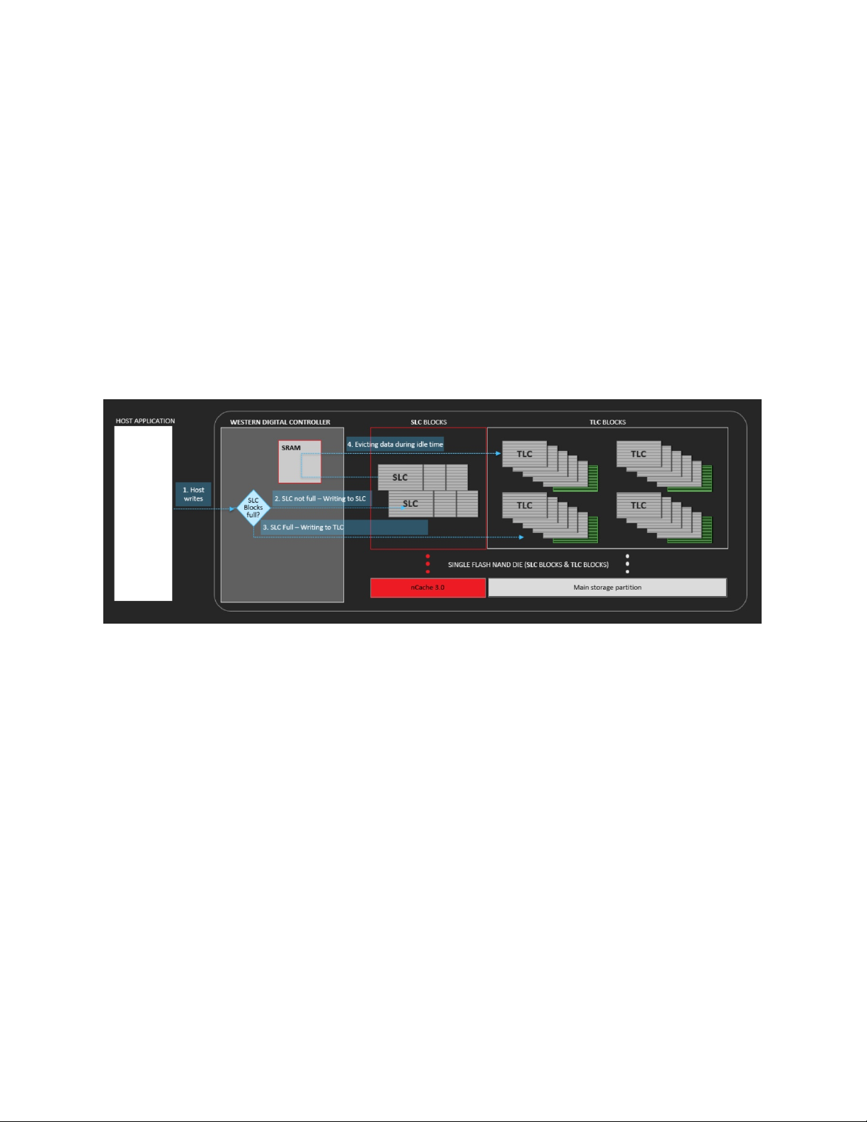
2.4.5 SLC Cache - nCache 3.0
The nCache 3.0 is a pool of X1 (SLC) blocks for sequential and random host
operations. These X1 blocks are used as write cache to accumulate and consolidate all
writes at high speed.
The PC SN730 NVME SSD utilize the nCache 3.0 tiered caching which further improves
performance and power efficiently by introducing several enhancements as:
Direct TLC (write) Access - improves sustain-write-access power efficiency and
write throughput.
Enhanced Evacuation Policy - improves the write-burst access speed.
As mentioned above, the nCache 3.0 works in the background to flush them into the
larger X3 (TLC) storage blocks and uses optimized write transaction sizes to maximize
endurance. Once the SLC blocks are full the Drive will continue to program TLC
blocks directly, and will re-locate the data from SLC to TLC on Idle times.
Figure 2-1. Western Digital PC SN730 NVMe SSD Tiered Caching Technology
2.4.6 Error Correction Layers
The PC SN730 NVME SSD advanced Error Correction and Data recovery mechanism
constructed from multi layers of protection:
Multi Gear LDPC Engine – The PC SN730 NVME SSD LDPC use Multi-Gear
Hardware LDPC Engine tailored for Western Digital 3D NAND. The ultra-low
power and high speed - Gear1 Mode, help reduce the overall power consumed by
the LDPC during reads and writes.
Hardware DSP and Soft Decode – Hardware accelerators used for enhanced Error
Correction; at high BER rates.
XOR Recovery – The XOR Recovery is an extreme and rare protection layer. It is a
RAID-Like protection and is able to recovery multi-pages at need.
- 11 - 00-01-WW-04-00047
Page 12

General Product Specifications
3.0 GENERAL PRODUCT SPECIFICATIONS
3.1 Interface
The PC SN730 NVME SSD is a PCI Express Gen3 x4 SSD.
Complies with:
PCI Express 3.0 up to four lanes, and a bit rate of 2.5Gbps or 5Gbps or 8Gbps
Configurable Lane width: x1, x2 and x4
NVM Express Rev 1.3
3.2 Hardware Configuration
Table 3-1 provides the basic hardware configuration values for the PC SN730 NVME
SSD.
Table 3-1. PC SN730 NVMe SSD Hardware Configuration
SSD Capacity Form Factor NAND Technology Memory
256GB M.2 2280-S3-M BiCS4 256Gb 2P X3 2 x 4D BGA
512GB M.2 2280-S3-M BiCS4 256Gb 2P X3 2 x 8D BGA
1024GB M.2 2280-S3-M BiCS4 256Gb 2P X3 2 x 16D BGA
3.3 Capacity
Table 3-2. Western Digital CL SN730 NVMe SSD Capacity Specification
Unformatted Capacity
256GB 500,118,192 M.2 2280-S3-M
512GB 1,000,215,216 M.2 2280-S3-M
1024GB 2,000,409,264 M.2 2280-S3-M
1
1 gigabyte (GB) = 1 billion bytes. Some of the listed capacity is used for formatting and other functions,
and thus is not available for data storage.
2
1 Sector = 512 bytes. LBA count based on IDEMA standard.
1
Sectors in LBA Mode
2
Available Form Factors
- 12 - 00-01-WW-04-00047
Page 13

4.0 PERFORMANCE
Table 4-1 includes the PC SN730 NVMe SSD performance in a system that supports PCI
Express Gen3 x4, FOB in CDM and PC Mark Vantage.
Table 4-1. Western Digital PC SN730 NVMe SSD M.2 2280 Performance
Parameter Queue Depth / Threads 256GB 512GB 1024GB
Performance
Sequential Read 128KB MB/s
Sequential Write 128KB MB/s
Random Read 4KB (32QD) IOPS
Random Write 4KB (32QD) IOPS
1
Test Conditions: Performance is measured by CrystalDiskMark 6.0.2 using 1GB LBA range. Windows 10 using
Microsoft driver build 17134.112, Secondary drive FOB. ASUS Z270-A platform with Intel® i7-7700K 4.2Ghz processor.
C-state On.
1
1
1
1
QD=32, T = 1 3,150 3,400 3,400
QD=32, T = 1 2,100 2,700 3,100
QD=32, T = 8 270,000 460,000 550,000
QD=32, T = 8 280,000 400,000 550,000
- 13 - 00-01-WW-04-00047
Page 14

Power Characteristics
5.0 POWER CHARACTERISTICS
5.1 Supply Voltage
Table 5-1. Western Digital PC SN730 NVMe SSD Supply Voltage
Parameter Specification
Input Voltage M.2 2280 3.3V ± 5%
Maximum Ripple 100mV (peak to peak), 100Hz to 6MHz
Maximum Supply Rise Time 100ms
5.2 Average Active-Power Consumption
1
The average active-power consumption is defined as the blended read/write/idle
power used by the drive while in operation with a commonly used operating system.
It is measured using the MobileMark™ benchmark, average 5 seconds. During this test
Microsoft StorNVMe driver triggers non-operative low power state.
This benchmark simulates the typical usage of user applications in a Windows
environment, providing a reproducible test for measuring average active-power
consumption.
Table 5-2. Western Digital PC SN730 NVMe SSD Average Active-Power Consumption
Form Factor Input Voltage Test Suite Unit 256GB 512GB 1024GB
M.2 2280 3.3V ± 5% Productivity mW 100 100 100
5.3 Operating Power Consumption – Average Maximum
Average maximum operating power consumption is measured while the PC SN730
NVME SSD is continuously processing sequential read and write commands (tested
separately) for at least 1 minute, with a transfer size of 256 sectors per command
(128KB), queue depth of 32 and 1 thread. The sampling interval is 125 milliseconds.
This benchmark is designed to test the worst-case scenario, when continuous power
is required by the PC SN730 NVME SSD during long read or write command
sequences.
Table 5-3. Western Digital PC SN730 NVMe SSD Average Max Power Consumption
2
Form Factor Input Voltage Test Unit 256GB 512TB 1024GB
Read
M.2 2280 3.3V ± 5%
Write
1
Measured using MobileMark™ 2014 on ASUS B9440UA, i5-7200U, Windows 10 RS5 1809 build 17763.529, iRST
15.44.0.1010, primary drive. Average power.
2
Measured at 25°C. Power consumption can vary due to input voltage and ambient temperature variation.
- 14 - 00-01-WW-04-00047
mW 3,900 4,700 5,200
A 1.18 1.42 1.58
mW 2,900 4,100 5,400
A 0.88 1.24 1.64
Page 15

Power Characteristics
5.4 Peak Power and In-Rush Current
Peak power consumption is the maximum instantaneous power consumption
measured while the PC SN730 NVME SSD is continuously processing sequential read
and write commands (tested separately) for at least 1 minute, with a transfer size of
256 sectors per command (128KB), queue depth of 32 and 1 threads. The sampling
interval is 10µs. This benchmark is designed to test the worst-case scenario, when
continuous power is required by the PC SN730 NVME SSD during long read or write
command sequences.
Maximum in-rush current refers to the maximum instantaneous power consumption of
the PC SN730 NVME SSD drive after a power cycle until all voltage rails required for
operation are stabilized to their nominal values on the drive. The sampling interval is
10µs.
Table 5-4. Western Digital PC SN730 NVMe SSD Peak Power and In-Rush Current
Form Factor Input Voltage Test Unit 256GB 512GB 1024GB
Peak Power
(10us)
M.2 2280 3.3V ± 5%
Max In-Rush
mW 5,610 6,270 7,590
A 1.7 1.9 2.3
mW 6,930 6,930 6,930
A 2.1 2.1 2.1
5.5 NVMe Power Management
The PC SN730 NVME SSD supports NVMe power management. Product Identify
reports 5 NVMe power modes as detailed below.
L1.2 mode enabled and asynchronously controlled by the PCI Express layer.
Table 5-5 details the power consumption and performance per power state. Power
consumption and performance are measured during sustained sequential write or
sustained sequential read as defined in Section 4.0 Performance on page 13.
Table 5-5. PC SN730 NVMe SSD Power Consumption and Performance Per NVMe Power State
Power
Mode
PS0 Full Performance 256GB: 3,100
Device State
Sustained Sequential
Read/Write up to [MB/s] Avg Power
512GB: 3,400
1024GB: 3,400
256GB: 3.9W
512GB: 4.7W
1024GB: 5.4W
Entry Latency
(ENLAT)
--- ---
Exit Latency
(EXLAT)
PS1 Light Throttling 256GB: 1,600
512GB: 1,600
1024GB: 1,600
PS2 Heavy Throttling 256GB: 350
512GB: 350
1024GB: 350
PS3 Non-Operational,
Rapid recovery
PS4 Non-Operational,
Slow Recovery
256GB: 3.3W
512GB: 3.5W
1024GB: 3.7W
256GB: 2.0W
512GB: 2.1W
1024GB: 2.2W
--- 256GB: 30mW
512GB: 30mW
1024GB: 30mW
--- 256GB: 3.5mW
512GB: 3.5mW
1024GB: 3.5mW
- 15 - 00-01-WW-04-00047
---- ----
---- ----
4ms 10ms
4.5ms 35ms
Page 16

Power Characteristics
5.6 Graceful Power-off Requirements
On most operating systems, Write Cache is enabled by default. This feature is not
specific to Western Digital SSD products. There may be data residing in the PC SN730
NVME SSD cache that have not been written to the flash memory. To ensure that the
data is properly committed to flash memory, the PC SN730 NVME SSD requires the
host to write 01b (normal shutdown) to the Shutdown Notification (CC:SHN)
field. This command instructs the PC SN730 NVME SSD to write all of its volatile data
cache to flash memory and returns a GOOD status to the host after its successful
completion. This command is handled transparently by most operating systems
during the shutdown sequence (for example, hibernation, shutdown, and standby.)
However, if power is lost without warning – leading to an ungraceful shutdown – data
loss may occur. This may also lead to a longer power-on time for the subsequent
power-up.
- 16 - 00-01-WW-04-00047
Page 17

6.0 THERMAL THROTTLING
6.1 Self-Thermal Throttling
In order to protect the integrity of the data and prevent excessive heat dissipation,
the PC SN730 NVME SSD utilizes several component temperature sensors (junction
temperature) to monitor the SSD critical components temperatures. If a sensor
temperature rises above the allowable limit, system performance is lowered until the
temperature decreases to an acceptable level. The device returns to full performance
when the temperature returns to a normal range.
Table 6-1 describes the performance results, while thermal throttling is activated.
Table 6-1. Western Digital PC SN730 NVMe SSD Performance Under Thermal Throttling
Thermal Throttling
PC SN730
NVMe SSD
Self-Throttling Mode
Power [W] 1.7W 1.7W 1.7W 1.7W 1.7W 1.7W
1
Performance
1
While during self-throttling mode PC SN730 NVME SSD is keeping the power value flat; performance may
be varied between devices due to process variation.
[MB/s]
Sequential
6.2 Denial of Service
To avoid data corruption, and as a last protection measure, if the NAND temperature
increases above the maximum allowed then the device will enter a denial of service
state. A recovery to functional mode is only by a full power cycle.
256GB 512GB 1TB
Read
40 40 40 40 40 40
Sustained
Sequential
Write
Sequential
Read
Sustained
Sequential
Write
Sequential
Read
Sustained
Sequential
Write
- 17 - 00-01-WW-04-00047
Page 18

7.0 ENDURANCE
The endurance of the PC SN730 NVME SSD is calculated using JEDEC client workload
(JESD219), unconnected to power.
Endurance is a direct function of user workload and access pattern. It is defined in terms of
Terabytes Written (TBW). Refer to Table 7-1 below.
Table 7-1. Western Digital PC SN730 NVMe SSD Endurance
Parameter 256GB 512GB 1024GB
Drive Endurance Data Retention I Year @ 30°C 200 TBW 300 TBW 400 TBW
Endurance
- 18 - 00-01-WW-04-00047
Page 19

8.0 SECURITY
8.1 Password Lock Through TCG Pyrite 2.0
The Western Digital PC SN730 NVMe SSD supports password locking of user data as
defined in the following TCG specification: TCG Storage Security Subsystem Class:
Pyrite. Specification Version 2.0.
The Western Digital PC SN730 NVMe SSD implementation of TCG Pyrite includes the
following capabilities and characteristics:
Provides a mechanism that locks access to the entire user media for NVMe read
TCG Pyrite features:
Security
and write commands. When configured, access is locked automatically upon
device power cycle.
– 1 global locking range
– Separate flags to control Read and Write locking
– 1 admin authority, 2 user authorities
– Revert
– TCG DataStore table size is 128KB
– Supported Pyrite authorities:
One SID to activate TCG security
One admin authority to configure locking and permissions
Up to two regular user authorities to unlock read and write commands
Block SID is supported in accordance to TCG Storage Feature Set: Block SID
Authentication
PSID Revert feature for TCG Pyrite 2.0:
– Level 0 discovery for PSID Extension Feature Descriptor
– Physical Presence SID (PSID) is supported in accordance to TCG Storage Opal
SSC Feature Set: PSID.
– PSID Revert erases data using the Block Erase method
System BIOS shall request and submit user password to unlock device during
system boot
Device supports up to 5 authentication attempts with wrong password. After
that, it requires power cycle before accepting a new authentication
Unlock password is not stored in device as a plain text, cryptographic digest is
used instead
By default, device is shipped with TCG security in inactive state and default
credentials of SID authority. BIOS shall support the TCG Block SID Authentication
feature to prevent malicious host applications from taking control over device
security with default SID credentials.
Encryption of user data and MBR shadowing are not supported.
- 19 - 00-01-WW-04-00047
Page 20

8.2 Secure Erase
Western Digital PC SN730 NVMe SSD supports sanitization of user data using the
Format NVM command in one of the following modes:
1. The No Secure Erase mode implements logical erase of user data: cleanup of FTL
tables marks all blocks as unallocated. Subsequent read commands return zeroes
for erased data.
2. The User Data Erase mode implements physical erase of user data with NAND
block erase operation. The process covers all user LBAs including any spare and
re-allocated blocks.
3. The Crypto Erase implements cryptographic erase of user data by eradicating its
encryption key. The Crypto Erase mode is not supported on Non-SED devices.
Western Digital PC SN730 NVMe SSD SED supports sanitization of user data using the
Sanitize command in one of the following modes: Block Erase and Crypto Erase. The
Overwrite mode is not supported.
Sanitization of locked devices is supported on PC SN730 NVME SSD SED with PSID
revert command.
Table 8-1 summarizes sanitization modes and their result:
Security
Table 8-1. Western Digital PC SN730 NVMe SSD Format NVM Modes and Results
PC SN730 NVMe SSD, Non-SED
Command Mode Operations Data at Rest Read Result
Format NVM 000b (No Secured Erase) FTL Cleanup Last Written Zeros
001b (User Data Erase) FTL Cleanup,
Block Erase
010b (Crypto Erase) N/A N/A N/A
Erased Zeros
8.3 Security of Read-Only Mode
Device enters Read-Only mode upon reaching End-of-Life conditions for user media.
In this mode, it stops accepting commands that might write user or system data.
Format NVM in the User Data Erase and the Crypto Erase mode is also supported
when device turns read only mode. It provides a secure option to erase all user data
before disposal of the device or before returning it for FA. Successful status returned
for the command is an indication of complete sanitization of user data. If device fails
to complete the process, sanitization should be addressed by physical destroy
methods, e.g. shredding.
Device preserves TCG locking settings as configured before transition to Read-Only
mode. Host application shall be ready that NVMe commands Format NVM and Sanitize
are aborted when device is Write-locked. Host shall unlock device with valid user
password before applying the command. Alternatively, it shall use sanitization
commands of the active TCG Opal protocol: TCG Revert.
- 20 - 00-01-WW-04-00047
Page 21

Security
8.4 Secure Field Firmware Update (FFU)
The genuine Western Digital firmware update image is encrypted and signed. The
RSA digital signature algorithm with 2048-bit key is used for signing of the file, while
AES-CBC-256 algorithm is used for encryption.
Device automatically verifies signature of a firmware update image during FFU and
rejects images that fails the procedure. Root certificate is provisioned to permanent
eFuse storage in SSD controller during device manufacturing. FW signing process in
WD relies on HSM-based signing server for storage of private keys to guaranty
protection of the key leakage and auditability of FW releases.
Device implements no interface to update device firmware that bypasses regular FFU
commands and to disable digital signature verification.
8.5 Secure Boot
Device verifies digital signatures of firmware images loaded from NAND Flash storage
before running them on CPU during boot. Signatures cover all parts of stored
firmware including boot loader. Boot loader itself is verified by ROM, then it verifies
other parts. If firmware verification fails, device enters fail mode when it does not
provide access to user data.
Secure Boot uses RSA digital signature algorithm with 2048-bit keys. FW signing
process in WD relies on HSM-based signing server for storage of private keys. SSD
controller includes HW acceleration for RSA calculations to make sure that signature
verification does not cause significant delays for device initialization.
8.6 Secure RMA
All Western Digital PC SN730 NVMe SSD devices implement hardware locks for debug
access to SSD controller and for any vendor-specific diagnostic commands.
Removing these locks is limited only to authorized engineers in WD facilities. They
authenticate device RMA with RSA challenge-request protocol that uses WD HSMbased signing server to generate unlock tokens. Public key to verification of the
process is provisioned to device during manufacturing with root certificate burned in
controller eFuse.
- 21 - 00-01-WW-04-00047
Page 22

Physical Specifications
9.0 PHYSICAL SPECIFICATIONS
9.1 M.2 2280 Form Factor
The M.2 2280 form factor complies with PCI Express M.2 (NGFF) Electromechanical
Specification, rev. 1.1.
Table 9-1. PC SN730 NVMe SSD M.2 2280 Form Factor Mechanical Specifications
Parameter Specification
Type 256GB: M.2 2280 S3-M
Width 22 ± 0.15mm
Length 80 ± 0.15mm
PCB Thickness 0.80 ± 0.08mm
Component Height 1.5mm
Thickness (max) 256GB: 2.23mm
Typical Weight 7.3±0.5gr
Figure 9-1. Top and side view of the PC SN730 NVMe SSD
512GB: M.2 2280 S3-M
1024GB: M.2 2280 S3-M
512GB: 2.38mm
1024GB: 2.38mm
- 22 - 00-01-WW-04-00047
Page 23

Environmental Specifications
10.0 ENVIRONMENTAL SPECIFICATIONS
10.1 Temperature
Table 10-1. Western Digital PC SN730 NVMe SSD Temperature Specification
Parameter Specifications
Non-operational
1
Operational temperature is defined as temperature reported by the drive. Note that drive temperature
readings are expected to be higher than ambient temperature when the SSD is placed inside a system.
2
Non-operational storage temperature does not guarantee data retention.
10.2 Humidity
Table 10-2. Western Digital PC SN730 NVMe SSD Humidity Specification
Operational
Non-Operational
10.3 Vibration
Operational
1
2
Parameter Specifications
Humidity (Non-condensation) 5% to 95%
Maximum Wet Bulb 30°C
Humidity (Non-condensation) 5% to 95%
Maximum Wet Bulb 40°C
0°C to 70°C
-55°C to 85°C
Table 10-3. Western Digital PC SN730 NVMe SSD Vibration Specification
Non-Operation Vibration 4.9G
Operating Vibration 5G
10.4 Shock
Table 10-4. Western Digital PC SN730 NVMe SSD Shock Specification
Non-Operational Shock
Parameter Specifications
, 7 to 800Hz, 15min/axis on 3 axes
RMS
, 10 to 2,000Hz, 15min/axis on 3 axes
RMS
Parameter Acceleration Force
Operating and
1500G,0.5ms, half sine, 3 pulses x 6 surfaces
- 23 - 00-01-WW-04-00047
Page 24

10.5 Altitude
Table 10-5. Western Digital PC SN730 NVMe SSD Altitude Specification
Operational/Non-operational -1500ft (-457m) to 40,000ft (12,192m)
Environmental Specifications
Parameter Specifications
10.6 Electrostatic Discharge (ESD)
Table 10-6. Western Digital PC SN730 NVMe SSD ESD Specification
Parameter Voltage
Contact ±4kV
Air 8kV
10.7 Acoustics
The PC SN730 NVMe SSD does not generate any acoustic noise (0dB).
10.8 Chemical Restrictions
The Western Digital PC SN730 NVMe SSD complies with the European Union’s
Restriction on Use of Hazardous Substances in Electrical and Electronic Equipment
(EU RoHS) Directive 2011/65/EC and European Union’s Registration, Evaluation,
Authorization and Restriction of Chemicals (REACH), Regulation (EC) 1907/2006.
Western Digital PC SN730 complies with the European Community Directive 2012/
19/EU on Waste Electrical and Electronic Equipment (WEEE).
1
It also complies with China’s management methods for controlling pollution by
electronic information products (China RoHS).
1
Tested per IEC 61000-4-2 Standard.
- 24 - 00-01-WW-04-00047
Page 25

Environmental Specifications
10.9 Regulatory Agency Approvals and Declarations
PC SN730 meets the standards of the following regulatory agencies:
Federal Communication Commission: Verified to comply with FCC Rules for
Radiated and Conducted Emission, Part 15, Subpart B, for Class B Equipment.
This equipment has been tested and found to comply with the limits for a class B
digital device, pursuant to part 15 of the FCC Rules. These limits are designed to
provide reasonable protection against harmful interference in a residential
installation. This equipment generates, uses and can radiate radio frequency
energy and if not installed and used in accordance with the instructions, may
cause harmful interference to radio communications. However, there is no
guarantee that interference will not occur in a particular installation. If this
equipment does cause harmful interference to radio or television reception,
which can be determined by turning the equipment off and on, the user is
encouraged to try to correct the interference by one or more of the following
measures:
– Reorient or relocate the receiving antenna.
– Increase the separation between the equipment and receiver.
– Connect the equipment into an outlet on a circuit different from that to which
the receiver is connected.
– Consult the dealer or an experienced radio/TV technician for help.
Canada EMI Compliance: Per ICES-003 Issue 5, Class B
CE Compliance for Europe Countries and Morocco: Verified to comply with
EN55032:2015 for RF Emissions and EN55024:1998, A1:2001 + A2:2003, EN61000-32:2000, EN61000-3-3:1995 + A1:2001 for Generic Immunity as applicable.
Verified to meet or exceed Directive of Electromagnetic Compatibility 2014/30/
EU and Safety Low Voltage Directive 2014/35/EU.
RCM Compliance for Australia and New Zealand: Verified to comply with AS/
NZ3548 for RF Emissions as required by the Australian Communications Authority.
Korean KC Mark: Registered as a Class-B product with the South Korean Ministry
of Information and Communication.
Taiwan BSMI ROHS Compliance: Certified as a Class-B product with the Bureau of
Standards Metrology and Inspection (BSMI ROHS).
Voluntary Control Council for Interference (VCCI): Verified to comply with VCCI
V-2 (V-3 Technical Requirements), the Voluntary Control Council for Interference
by Information Technology Equipment.
CB-Scheme Safety Standard: Verified safety compliance per IEC 60950-1 (IEC
System for Mutual Recognition of Test Certificates for Electrical Equipment
(IECEE)).
- 25 - 00-01-WW-04-00047
Page 26

Environmental Specifications
Underwriters Laboratories for USA and Canada product safety: Bi-National UL
Standard CAN/CSA-C22.2 No. 60950/UL 60950-1 Standard for Safety of
Information Technology Equipment, including Electrical Business Equipment.
EU Safety Compliance: IEC 60950-1 per EN 60950-1, Standard for Safety of
Information Technology Equipment, including Electrical Business Equipment.
- 26 - 00-01-WW-04-00047
Page 27

Reliability Characteristics
11.0 RELIABILITY CHARACTERISTICS
11.1 Error Rate
The non-recoverable error rate is 1 error per 1017 bits read.
11.2 Mean Time to Failure (MTTF)
Mean Time to Failure (MTTF) is the reliability figure most often used for electronic
equipment. The Western Digital PC SN730 NVMe SSD has an estimated MTTF using a
prediction methodology based in accordance with the Telcordia Special Report SR-
332. The prediction is based on a Parts Stress Analysis.
Quality levels were defined as industrial grade (I) for all of the components. The
detailed prediction for the system was performed at a temperature of 25°C in a GB
(ground, benign) environment.
Table 11-1 summarizes the estimated MTTF results for each capacity.
Table 11-1. Western Digital PC SN730 NVMe SSD MTTF
Capacity Condition MTTF (Hours)
256GB Telcordia SR-332, GB, 25°C 1,752,000
512GB Telcordia SR-332, GB, 25°C 1,752,000
1024GB Telcordia SR-332, GB, 25°C 1,752,000
1
1
Based on internal testing using Telcordia stress part testing.
- 27 - 00-01-WW-04-00047
Page 28

Windows Device Certifications
12.0 WINDOWS DEVICE CERTIFICATIONS
12.1 HCK Certification
The PC SN730 NVMe SSD certified with Windows HCK (Hardware Certification Kit) for
Windows 7.
Category: Device
Product Type: Hard Drive
12.2 HLK Certification
The PC SN730 NVMe SSD certified with Windows HLK (Hardware Lab Kit) for
Windows 10.
Category: Device
Product Type: Hard Drive
- 28 - 00-01-WW-04-00047
Page 29

13.0 INTERFACE
13.1 Supported Standards
The PC SN730 NVMe SSD complies with the following standards:
PCI Express® Base Specification Revision 3.0
13.2 Pin Assignments - M.2 2280, M Key
Table 13-1. M.2 Pin Assignments
Interface
Pin # Function Pin # Function
1 GND 2 3.3V
3 GND 4 3.3V
5 PETn3 6 NC
7 PETp3 8 PLN
9 GND 10 LED/DAS
11 PERn3 12 3.3V
13 PERp3 14 3.3V
15 GND 16 3.3V
17 PETn2 18 3.3V
19 PETp2 20 NC
21 GND 22 NC
23 PERn2 24 NC
25 PERp2 26 NC
27 GND 28 NC
29 PETn1 30 NC
31 PETp1 32 NC
33 GND 34 NC
35 PERn1 36 NC
37 PERp1 38 NC
39 GND 40 NC
41 PETn0 42 NC
43 PETp0 44 NC
45 GND 46 NC
47 PERn0 48 NC
49 PERp0 50 PERST#
51 GND 52 CLKREQ#
53 REFCLKn 54 NC
55 REFCLKp 56 NC
57 GND 58 NC
59 M key 60 M key
61 62
63 64
65 66
67 NC 68 NC
69 NC 70 3.3V
71 GND 72 3.3V
73 GND 74 3.3V
75 GND
- 29 - 00-01-WW-04-00047
Page 30

Supported NVMe Commands and Features
14.0 SUPPORTED NVME COMMANDS AND FEATURES
14.1 NVMe Command Set
PC SN730 NVMe SSD support NVMe 1.3 standard command set and the following
configurations:
1 Namespace
64 Queues
8 Async. Events Notifications
Table 14-1. Admin Commands
Command Name Opcode Comment
Delete I/O Submission Queue 00h
Create I/O Submission Queue 01h
Get Log Page 02h
Delete I/O Completion Queue 04h
Create I/O Completion Queue 05h
Identify 06h
Abort 08h
Set Features 09h
Get Features 0Ah
Asynchronous Event Request 0Ch Maximum of 8.
Firmware Commit 10h
Firmware Image Download 11h
Device Self-Test 14h
Format NVM (User Data Erase) 80h
Security Send 81h
Security Receive 82h
Sanitize 84h
Table 14-2. NVM Commands
Command Name Opcode Comment
Flush 00h
Write 01h
Read 02h
Write Uncorrectable 04h
Compare 05h
Write Zeros 08h
Dataset Management 09h
- 30 - 00-01-WW-04-00047
Page 31

Supported NVMe Commands and Features
Table 14-3. Set Features/Get Features
Command Name Opcode Comment
Feature Identifiers – Mandatory Arbitration
Feature Identifiers – Mandatory Power Management
Feature Identifiers – Optional LBA Range Type
Feature Identifiers – Mandatory Temperature Threshold
Feature Identifiers – Mandatory Error Recovery
Feature Identifiers – Optional Volatile Write Cache
Feature Identifiers – Mandatory Number of Queues
Feature Identifiers – Mandatory Interrupt Coalescing
Feature Identifiers – Mandatory Interrupt Vector Configuration
Feature Identifiers – Mandatory Write Atomicity
Feature Identifiers – Mandatory Asynchronous Event Configuration
Feature Identifiers – Optional Autonomous Power State Transition
Feature Identifiers – Optional Host Controlled Thermal Management
Feature Identifiers – Optional Non-Operational Power State Configuration
Feature Identifiers - Optional Telemetry
Feature Identifiers - Optional Sanitize Operations
14.2 Identify Controller Response
Table 14-4 defines the specifics of the Identify Controller returned by the PC SN730
NVMe SSD.
Table 14-4. Controller Capabilities and Features
Bytes Field Value Comments
01:00 PCI Vendor ID (VID) 15B7h
03:02 PCI Subsystem Vendor ID
(SSVID)
23:04 Serial Number (SN) Variable Unique serial number in ASCII
63:24 Model Number (MN) “WDC PC SN730” and
71:64 Firmware Revision (FR) Variable Format: 8 numeric digits
72 Recommended Arbitration
Burst (RAB)
75:73 IEEE OUI Identifier (IEEE) 001B44h
76 Controller Multi-Path I/O and
Namespace Sharing Capabilities (CMIC)
15B7h
SKU
4h
0h 7-3 Reserved
2 0 = PCI Function
1 0 = Single Controller
0 0 = Single PCIe Port
- 31 - 00-01-WW-04-00047
Page 32

Supported NVMe Commands and Features
Table 14-4. Controller Capabilities and Features (Continued)
Bytes Field Value Comments
77 Maximum Data Transfer Size
7h 512KB
(MDTS)
79:78 Controller ID (CNTLID) 2017h
83:80 Version (VER) 10300h
87:84 RTD3 Resume Latency
7A120h 500,000us
(RTD3R)
91:88 RTD3 Entry Latency
F4240h 1,000,000us
(RTD3E)
95:92 Optional Asynchronous Events
200h
Supported (OAES)
99:96 Controller Attributes
2h
(CTRATT)
239:100 Reserved 0h
255:240 NVMe Management Interface 0h
Table 14-5. Admin Command Set Attributes and Optional Controller Capabilities
Bytes Field Value Comments
257:256 Optional Admin Command
Support (OACS)
17h Supported commands:
Security Send and Security
Receive
Format NVM
Firmware Commit and
Firmware Image Download
Device Self-Test
15-9 Reserved
8-5 0=not supported
4 1 = Device Self-test com-
mand is supported
3 0 = no support for the
Namespace Management
and Namespace Attachment commands
2 1 = Firmware Commit and
Firmware Image Download commands are supported
1 1 = Format NVMe com-
mand is supported
0 1 = Security Send and
Security Receive commands are supported
258 Abort Command Limit (ACL) 4h 5 Abort commands supported
259 Asynchronous Event Request
7h 8 AERs supported
Limit (AERL)
260 Firmware Updates (FRMW) 14h 7-5 Reserved
4 1 = firmware activation
without a reset is supported
3-1 010 = 2 firmware slots are
supported
0 1 = slot 1 is read only
0 = slot 1 is read/write
- 32 - 00-01-WW-04-00047
Page 33

Supported NVMe Commands and Features
Table 14-5. Admin Command Set Attributes and Optional Controller Capabilities (Continued)
Bytes Field Value Comments
261 Log Page Attributes (LPA) 1Eh Command Effects log page
262 Error Log Page Entries (ELPE) FFh 256 entries supported
supported
7-3 Reserved
3 1 = support for Telemetry
Host-Initiated and Telemetry Controller-Initiated
log pages and sending
Telemetry log
2 1 = support for extended
data for Get Log Page
1 1 = Command Effects Log
page is supported
0 0 = no support for
SMART/Health information log page on a per
namespace basis
263 Number of Power States Sup-
port (NPSS)
264 Admin Vendor Specific Com-
mand Configuration (AVSCC)
265 Autonomous Power State Tran-
sition Attributes (APSTA)
267:266 Warning Composite Tempera-
ture Threshold (WCTEMP)
269:268 Critical Composite Tempera-
ture Threshold (CCTEMP)
271:270 Maximum Time for Firmware
Activation (MTFA)
275:272 Host Memory Buffer Preferred
Size (HMPRE)
279:276 Host Memory Buffer Minimum
Size (HMMIN)
295:280 Total NVMe Capacity (TNVM-
CAP)
311:296 Unallocated NVM Capacity
(UNVMCAP)
4h
1h 7-1 Reserved
0 1 = All Admin Vendor Spe-
cific Commands use the
format as defined by
NVMe standard
1h Autonomous power state tran-
sitions supported
165h 357°K (83.85°C)
169h 361°K (87.85°C)
32h 5 seconds
0h
0h
256GB: 3B9E656000
512GB: 773C256000
1024GB: EE77A56000
0h
315:312 Replay Protected Memory
Block Support (RPMBS)
317:316 Extended Device Self-Test
Time (EDSTT)
318 Device Self-test Options
(DSTO)
319 Firmware Update Granularity
(FWUG)
321:320 Keep Alive Support (KAS) 0h
322:323 Host Controlled Thermal Man-
agement Attributes (HCTMA)
0h
256GB:1Ah
512GB:34h
1024GB:68h
1h
1h
1h
- 33 - 00-01-WW-04-00047
Page 34

Supported NVMe Commands and Features
Table 14-5. Admin Command Set Attributes and Optional Controller Capabilities (Continued)
Bytes Field Value Comments
324:325 Minimum Thermal Management
Temperature (MNTMT)
326:327 Maximum Thermal Manage-
ment Temperature (MXTMT)
328:331 Sanitize Capabilities (SANICAP) Non-SED: 2h
332:335 Host Memory Buffer Minimum
Descriptor Entry Size
(HMMINDS)
336:337 Host Memory Maximum
Descriptors Entries (HMMAXD)
511:338 Reserved 0h
Table 14-6. NVM Command Set Attributes
Bytes Field Value Comments
512 Submission Queue Entry Size
(SQES)
513 Completion Queue Entry Size
(CQES)
111h
165h
SED: 3h
0h
0h
66h 7-4 0110 = Maximum Submission
44h 7-4 0100 = Maximum Completion
Bit 1 = Support Block Erase
Bit 0 = Support Crypto Erase
(SED only)
Queue entry size is 6.
3-0 0110 = Required Submission
Queue entry size is 6.
Queue entry size is 4.
3-0 0100 = Required Completion
Queue entry size is 4.
515:514 Maximum Outstanding Com-
mands (MAXCMD)
519:516 Number of Namespaces (NN) 1h Supporting one Namespace
521:520 Optional NVM Command Sup-
port (ONCS)
523:522 Fused Operation Support
(FUSES)
524 Format NVM Attributes (FNA) Non-SED: 0h
525 Volatile Write Cache (VWC) 7h 7-1 Reserved
0h
5Fh 15-7 Reserved
5 0 = Reservations are not sup-
ported.
4 1 = Save field in the Set Fea-
tures command and the
Select field in the Get Features command are supported.
3 1 = Write Zero command is
not supported.
2 1 = Dataset Management
command is supported.
1 1 = Write Uncorrectable com-
mand is supported.
0 1 = Compare command is not
supported.
0h
SED: 4h
0 1 = Volatile write cache is
present.
- 34 - 00-01-WW-04-00047
Page 35

Supported NVMe Commands and Features
Table 14-6. NVM Command Set Attributes (Continued)
Bytes Field Value Comments
527:526 Atomic Write Unit Normal
(AWUN)
0h
529:528 Atomic Write Unit Power Fail
(AWUPF)
530 NVM Vendor Specific Com-
mand Configuration (NVSCC)
531 Reserved 0h
533:532 Atomic Compare and Write
Unit (ACWU)
535:534 Reserved 0h
539:536 SGL Support (SGLS) 0h
767:540 Reserved 0h
1023:768 NVM Subsystem NVMe Quali-
fied Name (SUBNQN)
1791:1024 Reserved 0h
2047:1792 NVMe over fabric identify. 0h
Table 14-7. Power State Descriptors
Bytes Field Value Comments
0h
1h 7-1 Reserved
0 1 = All NVM Vendor Specific
Commands use the format
defined in NVMe standard for
Vendor Specific commands.
0h
--
2079:2048 Power State 0 Descriptor
(PSD0)
MP 256GB:1F4
MP 512GB:226
MP 1024GB:258
MXPS: 0
NOPS: 0
ENLAT: 0
EXLAT: 0
RRT: 0
RRL: 0
RWT: 0
RWL: 0
IDLP: 0h
IPS: 00b
ACTP: 000h
APW: 000b
APS: 00b
255-184 Reserved
183-182 Active Power Scale (APS)
181-179 Reserved
178-176 Active Power Workload
(APW)
175-160 Active Power (ACTP)
159-152 Reserved
151-150 Idle Power Scale (IPS)
149-144 Reserved
143-128 Idle Power (IDLP)
127-125 Reserved
124-120 Relative Write Latency
(RWL)
119-117 Reserved
116-112 Relative Write Throughout
111-109 Reserved
108-104 Relative Read Latency (RRL)
103-101 Reserved
100-96 Relative Read Throughput
(RRT)
95-64 Exit Latency (EXLAT)
63-32 Entry Latency (ENLAT)
31-26 Reserved
25 Non-Operational State
(NOPS)
24 Max Power Scale (MXPS)
23-16 Reserved
15-00 Maximum Power (MP)
- 35 - 00-01-WW-04-00047
Page 36

Supported NVMe Commands and Features
Table 14-7. Power State Descriptors (Continued)
Bytes Field Value Comments
2111-2080 Power State 1 Descriptor (PSD1) MP:15Eh
2143-2112 Power State 2 Descriptor
(PSD2)
MXPS: 0b
NOPS: 0b
ENLAT: 0h
EXLAT: 0h
RRT: 0001b
RRL: 0001b
RWT: 0001b
RWL: 0001b
IDLP: 0h
IPS: 00b
ACTP: 0h
APW: 000b
APS: 00b
MP: 12Ch
MXPS: 0b
NOPS: 0b
ENLAT: 0b
EXLAT: 0b
RRT: 0010b
RRL: 0010b
RWT: 0010b
RWL: 0010b
IDLP: 0h
IPS: 00b
ACTP: 0h
APW: 000b
APS: 00b
255-184 Reserved
183-182 Active Power Scale (APS)
181-179 Reserved
178-176 Active Power Workload
(APW)
175-160 Active Power (ACTP)
159-152 Reserved
151-150 Idle Power Scale (IPS)
149-144 Reserved
143-128 Idle Power (IDLP)
127-125 Reserved
124-120 Relative Write Latency
(RWL)
119-117 Reserved
116-112 Relative Write Throughout
111-109 Reserved
108-104 Relative Read Latency (RRL)
103-101 Reserved
100-96 Relative Read Throughput
(RRT)
95-64 Exit Latency (EXLAT)
63-32 Entry Latency (ENLAT)
31-26 Reserved
25 Non-Operational State
(NOPS)
24 Max Power Scale (MXPS)
23-16 Reserved
15-00 Maximum Power (MP)
- 36 - 00-01-WW-04-00047
Page 37

Supported NVMe Commands and Features
Table 14-7. Power State Descriptors (Continued)
Bytes Field Value Comments
2175:2144 Power State 3 Descriptor
(PSD3)
MP 256GB:2BCh
MP 512GB:2BCh
MP 1024GB:3E8h
MXPS: 1b
NOPS:1b
ENLAT: FA0h
EXLAT: 2710h
RRT: 0011b
RRL: 0011b
RWT: 0011b
RWL: 0011b
IDLP: 0h
IPS: 0b
ACTP: 00h
APW: 000b
APS: 000b
255-184 Reserved
183-182 Active Power Scale (APS)
181-179 Reserved
178-176 Active Power Workload
(APW)
175-160 Active Power (ACTP)
159-152 Reserved
151-150 Idle Power Scale (IPS)
149-144 Reserved
143-128 Idle Power (IDLP)
127-125 Reserved
124-120 Relative Write Latency
(RWL)
119-117 Reserved
116-112 Relative Write Throughout
111-109 Reserved
108-104 Relative Read Latency (RRL)
103-101 Reserved
100-96 Relative Read Throughput
(RRT)
95-64 Exit Latency (EXLAT)
63-32 Entry Latency (ENLAT)
31-26 Reserved
25 Non-Operational State (NOPS)
24 Max Power Scale (MXPS)
23-16 Reserved
15-00 Maximum Power (MP)
2207:2176 Power State 4 Descriptor
(PSD4)
3071:2208 Power State Descriptors 5-31
(PSD5 – PSD31)
MP: 0019h
MXPS: 1b
NOPS:1b
ENLAT: FA0h
EXLAT: 9C40h
RRT: 0100b
RRL: 0100b
RWT: 0100b
RWL: 0100b
IDLP: 0h
IPS: 0b
ACTP: 00h
APW: 000b
APS: 000b
0h N/A
255-184 Reserved
183-182 Active Power Scale (APS)
181-179 Reserved
178-176 Active Power Workload
175-160 Active Power (ACTP)
159-152 Reserved
151-150 Idle Power Scale (IPS)
149-144 Reserved
143-128 Idle Power (IDLP)
127-125 Reserved
124-120 Relative Write Latency
119-117 Reserved
116-112 Relative Write Throughout
111-109 Reserved
108-104 Relative Read Latency (RRL)
103-101 Reserved
100-96 Relative Read Throughput
95-64 Exit Latency (EXLAT)
63-32 Entry Latency (ENLAT)
31-26 Reserved
25 Non-Operational State
24 Max Power Scale (MXPS)
23-16 Reserved
15-00 Maximum Power (MP)
(APW)
(RWL)
(RRT)
(NOPS)
- 37 - 00-01-WW-04-00047
Page 38

Supported NVMe Commands and Features
Table 14-8. Vendor Specific (VS)
Bytes Field Value Comments
4095:3072 Vendor Specific (VS) ---
14.3 Log Pages
PC SN730 NVMe SSD supports the following log pages:
Table 14-9. PC SN730 NVMe SSD Log Pages
Identifier Log Page Reference
01h Error Information NVM Express specification
02h SMART / Health Information NVM Express specification
03h Firmware Slot Information NVM Express specification
05h Commands Supported and Effects Log NVM Express specification
06h Device Self-Test NVM Express specification
07h Telemetry Host-Initiated NVM Express specification
08h Telemetry Controller-Initiated NVM Express specification
0Dh Persistent Event Log NVM Express specification
81h Sanitize Status NVM Express specification
CDh Vendor Specific Program/Erase Counters Refer to the following sections.
- 38 - 00-01-WW-04-00047
Page 39

Supported NVMe Commands and Features
14.3.1 SMART/Health Information (Log Identifier 02h)
Table 14-10. Western Digital PC SN730 NVMe SSD SMART/Health Information
Bytes Attribute Name Comment
0 Critical Warning
2:1 Composite Temperature Upon exiting low-power states, it
3 Available Spare
4 Available Spare Threshold
5 Percentage Used
47:32 Data Units Read
63:48 Data Units Written
79:64 Host Read Commands
95:80 Host Write Commands
111:96 Controller Busy Time
127:112 Power Cycles
143:128 Power On Hours
159:144 Unsafe Shutdowns
175:160 Media and Data Integrity Errors
191:176 Number of Error Information Log Entries
may take up to one second for
accurate temperature reporting.
195:192 Warning Composite Temperature Time
199:196 Critical Composite Temperature Time
14.3.2 Program/Erase SMART Counters (Log Identifier CDh)
Table 14-11. Program/Erase SMART Counters (Log Identifier CDh)
Bytes Attribute Name Comment
3:0 Minimum Program/Erase Counter for TLC
7:4 Maximum Program/Erase Counter for TLC
11:8 Average Program/Erase Counter for TLC
15:12 Minimum Program/Erase Counter for SLC
19:16 Maximum Program/Erase Counter for SLC
23:20 Average Program/Erase Counter for SLC
- 39 - 00-01-WW-04-00047
Page 40

15.0 ORDERING INFORMATION
Refer to the examples below as reference for ordering SKUs.
Table 15-1. PC SN730 NVMe SSD Ordering Information
Item Definition
SD Western Digital
G Generation: B
Ordering Information
SDG(I/F)FCT-CCCC-YYYY
(I/F) Interface and Security
F Form Factor: N - M.2 2280
C Controller: T – Triton 8CH Package
T NAND Technology: Y – BiCS4 256Gb 2P TLC
CCCC Capacity:
YYYY Customer Code Reference: None for Generic OEM
P- PCI Express (non-secure version)
Q- PCI Express (SED)
256G: 256G
512G: 512G
1T00: 1024G
Table 15-2 below shows the PC SN730 NVMe SSD SKUs.
Table 15-2. PC SN730 NVMe SSD Products SKUs
SKU Number Capacity Form Factor Type
SDBPNTY-256G 256GB M.2 2280 M-S3 non-SED
SDBPNTY-512G 512GB M.2 2280 M-S3 non-SED
SDBPNTY-1T00 1024GB M.2 2280 M-S3 non-SED
SDBQNTY-256G 256GB M.2 2280 M-S3 SED
SDBQNTY-512G 512GB M.2 2280 M-S3 SED
SDBQNTY-1T00 1024GB M.2 2280 M-S3 SED
- 40 - 00-01-WW-04-00047
Page 41

16.0 CONTACT INFORMATION
Visit https://www.westerndigital.com/products/internal-drives.
For further product information, contact your Western Digital Sales representative, or send
inquiries to OEMProducts@wdc.com.
Contact Information
- 41 - 00-01-WW-04-00047
Page 42

Western Digital
5601 Great Oaks Parkway
San Jose, CA 95119
U.S.A.
For service and literature:
support.wdc.com
www.westerndigital.com
800.ASK.4WDC North America
+800.6008.6008 Asia Pacific
00800.ASK.4WDEU Europe (toll free where available)
+31.88.0062100 Europe/Middle East/Africa
00-01-WW-04-00047
November 2019
 Loading...