

Page 1

November 09, 2018
W65C816S
8/16–bit Microprocessor
WDC reserves the right to make changes at any time without notice in order to improve design and supply
the best possible product. Information contained herein is provided gratuitously and without liability, to any
user. Reasonable efforts have been made to verify the accuracy of the information but no guarantee
whatsoever is given as to the accuracy or as to its applicability to particular uses. In every instance, it must
be the responsibility of the user to determine the suitability of the products for each application. WDC
products are not authorized for use as critical components in life support devices or systems. Nothing
contained herein shall be construed as a recommendation to use any product in violation of existing patents
or other rights of third parties. The sale of any WDC product is subject to all WDC Terms and Conditions of
Sales and Sales Policies, copies of which are available upon request.
Copyright (C) 1981-2018 by The Western Design Center, Inc. All rights reserved, including the right of
reproduction in whole or in part in any form.
Page 2

November 09, 2018
TABLE OF CONTENTS
1 INTRODUCTION ...................................................................................................... 5
1.1 Features of the W65C816S ......................................................................................................... 5
2 W65C816S FUNCTIONAL DESCRIPTION ............................................................. 6
2.1 Instruction Register (IR) ............................................................................................................. 6
2.2 Timing Control Unit (TCU) .......................................................................................................... 6
2.3 Arithmetic and Logic Unit (ALU)................................................................................................ 6
2.4 Accumulator (A) .......................................................................................................................... 6
2.5 Data Bank Register (DBR) .......................................................................................................... 6
2.6 Direct (D) ...................................................................................................................................... 7
2.7 Index (X and Y) ............................................................................................................................ 7
2.8 Processor Status Register (P) ................................................................................................... 7
2.9 Program Bank Register (PBR) ................................................................................................... 7
2.10 Program Counter (PC) ................................................................................................................ 7
2.11 Stack Pointer (S) ......................................................................................................................... 7
2.12 Pin Function Description .......................................................................................................... 10
2.13 Abort (ABORTB) ........................................................................................................................ 12
2.14 Address Bus (A0-A15) .............................................................................................................. 12
2.15 Bus Enable (BE) ........................................................................................................................ 12
2.16 Data/Bank Address Bus (D0-D7) ............................................................................................. 13
2.17 Emulation Status (E) ................................................................................................................. 13
2.18 Interrupt Request (IRQB) .......................................................................................................... 13
2.19 Memory Lock (MLB) .................................................................................................................. 13
2.20 Memory/Index Select Status (MX) ........................................................................................... 13
2.21 Non-Maskable Interrupt (NMIB) ............................................................................................... 14
2.22 Phase 2 In (PHI2) ....................................................................................................................... 14
2.23 Read/Write (RWB) ..................................................................................................................... 14
2.24 Ready (RDY)............................................................................................................................... 14
2.25 Reset (RESB) ............................................................................................................................. 15
2.26 Valid Data Address (VDA) and Valid Program Address (VPA) ............................................. 15
2.27 VDD and VSS ............................................................................................................................. 15
2.28 Vector Pull (VPB) ....................................................................................................................... 15
3 ADDRESSING MODES ......................................................................................... 16
3.1 Reset and Interrupt Vectors ..................................................................................................... 16
3.2 Stack ........................................................................................................................................... 16
3.3 Direct .......................................................................................................................................... 16
3.4 Program Address Space .......................................................................................................... 16
3.5 Data Address Space ................................................................................................................. 16
3.5.1 Absolute-a ................................................................................................................................. 17
3.5.2 Absolute Indexed Indirect-(a,x) ................................................................................................. 17
3.5.3 Absolute Indexed with X-a,x ...................................................................................................... 17
3.5.4 Absolute Indexed with Y-a,y ...................................................................................................... 17
3.5.5 Absolute Indirect-(a) .................................................................................................................. 18
3.5.6 Absolute Long Indexed With X-al,x ........................................................................................... 18
3.5.7 Absolute Long-al ........................................................................................................................ 18
3.5.8 Accumulator-A ........................................................................................................................... 18
3.5.9 Block Move-xyc ......................................................................................................................... 19
3.5.10 Direct Indexed Indirect-(d,x) .................................................................................................... 19
3.5.11 Direct Indexed with X-d,x ........................................................................................................ 20
3.5.12 Direct Indexed with Y-d,y ........................................................................................................ 20
2
Page 3

November 09, 2018
3.5.13 Direct Indirect Indexed-(d),y .................................................................................................... 20
3.5.14 Direct Indirect Long Indexed-[d],y ........................................................................................... 21
3.5.15 Direct Indirect Long-[d] ............................................................................................................ 21
3.5.16 Direct Indirect-(d) ..................................................................................................................... 21
3.5.17 Direct-d .................................................................................................................................... 22
3.5.18 Immediate-# ............................................................................................................................. 22
3.5.19 Implied-i ................................................................................................................................... 22
3.5.20 Program Counter Relative Long-rl ........................................................................................... 22
3.5.21 Program Counter Relative-r .................................................................................................... 22
3.5.22 Stack-s ..................................................................................................................................... 22
3.5.23 Stack Relative-d,s .................................................................................................................... 23
3.5.24 Stack Relative Indirect Indexed-(d,s),y.................................................................................... 23
4 TIMING, AC AND DC CHARACTERISTICS ......................................................... 25
4.1 Absolute Maximum Ratings ..................................................................................................... 25
4.2 DC Characteristics TA = -40°C to +85°C ................................................................................ 25
5 OPERATION TABLES........................................................................................... 29
6 RECOMMENDED W65C816S ASSEMBLER SYNTAX STANDARDS ................. 45
6.1 Directives ................................................................................................................................... 45
6.2 Comments .................................................................................................................................. 45
6.3 The Source Line ........................................................................................................................ 45
6.3.1 The Label Field .................................................................................................................... 45
6.3.2 The Operation Code Field ................................................................................................... 45
6.3.3 The Operand Field .............................................................................................................. 46
6.3.4 Comment Field .................................................................................................................... 48
7 Caveats ................................................................................................................. 49
7.1 Stack Addressing ...................................................................................................................... 50
7.2 Direct Addressing ..................................................................................................................... 50
7.3 Absolute Indexed Addressing ................................................................................................. 50
7.4 ABORTB Input ........................................................................................................................... 50
7.5 VDA and VPA Valid Memory Address Output Signals .......................................................... 50
7.6 DB/BA operation when RDY is Pulled Low ............................................................................ 51
7.7 MX Output .................................................................................................................................. 51
7.8 All Opcodes Function in All Modes of Operation .................................................................. 51
7.9 Indirect Jumps ........................................................................................................................... 51
7.10 Switching Modes ....................................................................................................................... 51
7.11 How Interrupts Affect the Program Bank and the Data Bank Registers ............................. 51
7.12 Binary Mode ............................................................................................................................... 52
7.13 Wait for Interrupt (WAI) Instruction .......................................................................................... 52
7.14 Stop-the-Clock (STP) Instruction ............................................................................................. 52
7.15 Co-Processor (COP) Signatures .............................................................................................. 52
7.16 WDM Opcode Use ..................................................................................................................... 52
7.17 RDY Pulled During Write .......................................................................................................... 52
7.18 MVN and MVP Affects on the Data Bank Register ................................................................. 52
7.19 Interrupt Priorities ..................................................................................................................... 53
7.20 Transfers from 8-Bit to 16-Bit, or 16-Bit to 8-Bit Registers ................................................... 53
7.21 Stack Transfers ......................................................................................................................... 53
7.22 BRK Instruction ......................................................................................................................... 53
7.23 Accumulator switching from 8-bit to 16-bit ............................................................................ 53
8 HARD CORE MODEL ........................................................................................... 54
8.1 W65C816 Core Information ...................................................................................................... 54
9 SOFT CORE RTL MODEL .................................................................................... 54
3
Page 4

November 09, 2018
9.1 W65C816 Synthesizable RTL-Code in Verilog HDL ............................................................... 54
10 ORDERING INFORMATION ............................................................................... 55
Table of Tables
Table 2-1 W65C816S Microprocessor Programming Model ............................................................................................... 9
Table 2-2 Pin Function Table ......................................................................................................................................... 12
Table 3-1 Addressing Mode Summary .......................................................................................................................... 24
Table 4-1 Absolute Maximum Ratings .......................................................................................................................... 25
Table 4-2 W65C816S AC Characteristics ...................................................................................................................... 27
Table 5-1 W65C816S Instruction Set-Alphabetical Sequence ......................................................................................... 29
Table 5-2 Emulation Mode Vector Locations (8-bit Mode) ............................................................................................... 30
Table 5-3 Native Mode Vector Locations (16-bit Mode) ................................................................................................... 30
Table 5-4 Opcode Matrix ................................................................................................................................................... 31
Table 5-5 Operation, Operation Codes, and Status Register ............................................................................................ 32
Table 6-1 Alternate Mnemonics ......................................................................................................................................... 46
Table 6-2 Address Mode Formats .................................................................................................................................... 47
Table 6-3 Byte Selection Operator ................................................................................................................................ 48
Table 7-1 Caveats ............................................................................................................................................................ 49
Table of Figures
Figure 2-1 W65C816S Internal Architecture Simplified Block Diagram .............................................................................. 8
Figure 2-2 W65C816S 40 Pin DIP Pinout ......................................................................................................................... 10
Figure 2-3 W65C816S 44 Pin PLCC Pinout ..................................................................................................................... 10
Figure 2-4 W65C816S 44 PIN QFP Pinout ....................................................................................................................... 11
Figure 4-1 General Timing Diagram ................................................................................................................................. 28
Figure 5-1 Bank Address Latching Circuit ...................................................................................................................... 44
4
Page 5

Advanced fully static CMOS design for low power
consumption and increased noise immunity
Wide operating voltage range, 1.8+/- 5%, 2.5+/5%, 3.0+/- 5%, 3.3+/- 10%, 5.0+/- 5% specified for
use with advanced low voltage peripherals
Emulation mode allows complete hardware and
software compatibility with 65xx designs
24-bit address bus provides access to 16 MBytes
of memory space
Full 16-bit ALU, Accumulator, Stack Pointer and
Index Registers
Valid Data Address (VDA) and Valid Program
Address (VPA) output for dual cache and cycle steal
DMA implementation
Vector Pull (VPB) output indicates when interrupt
vectors are being addressed
Abort (ABORTB) input and associated vector
supports processor repairs of bus error conditions
Low power consumption (300uA@1MHz)
Separate program and data bank registers allow
program segmentation or full 16 MByte linear
addressing
New Direct Register and stack relative addressing
provides capability for re-entrant, re-cursive and relocatable programming
24 addressing modes - 13 original W65C02S
modes with 92 instructions using 256 opcodes
Wait for Interrupt (WAI) and Stop-the-Clock (STP)
instructions further reduce power consumption,
decrease interrupt latency and allows synchronization
with external events
Co-Processor (COP) instruction with associated
vector supports co-processor configurations, i.e.,
floating point processors
Block move ability
November 09, 2018
1 INTRODUCTION
The W65C816S is a low power cost sensitive 8/16-bit microprocessor. The variable length instruction set
and manually optimized core size makes the W65C816S an excellent choice for low power System-on-Chip
(SoC) designs. The Verilog RTL model is available for ASIC design flows. WDC, a Fabless Semiconductor
Company, provides packaged chips for evaluation or volume production. To aid in system development,
WDC provides a Professional Software Development Kit (ProSDK) that is available for free download on a
trial basis, see www.westerndesigncenter.com for more information.
The WDC W65C816S is a fully static CMOS 16-bit microprocessor featuring software compatibility* with the
8-bit NMOS and CMOS 6500-series predecessors. The W65C816S extends addressing to a full 16
megabytes. These devices offer the many advantages of CMOS technology, including increased noise
immunity, higher reliability, and greatly reduced power requirements. A software switch determines whether
the processor is in the 8-bit "emulation" mode, or in the native mode, thus allowing existing systems to use
the expanded features.
As shown in the W65C816S Processor Programming Model, Table 2-1, the Accumulator, ALU, X and Y
Index registers, and Stack Pointer register have all been extended to 16 bits. A new 16-bit Direct Page
register augments the Direct Page addressing mode (formerly Zero Page addressing). Separate Program
Bank and Data Bank registers provide 24-bit memory addressing with segmented or linear addressing.
Four new signals provide the system designer with many options. The ABORTB input can interrupt the
currently executing instruction without modifying internal register, thus allowing virtual memory system
design. Valid Data Address (VDA) and Valid Program Address (VPA) outputs facilitate dual cache memory
by indicating whether a data segment or program segment is accessed. Modifying a vector is made easy by
monitoring the Vector Pull (VPB) output.
1.1 Features of the W65C816S
*Except for the BBRx, BBSx, RMBx, and SMBx bit manipulation instructions which do not exist for the
W65C816S
5
Page 6

November 09, 2018
2 W65C816S FUNCTIONAL DESCRIPTION
The W65C816S provides the design engineer with upward software compatibility from 8-bit W65C02S in
applications to 16-bit system application. In Emulation mode, the W65C816S offers many advantages,
including full software compatibility with W65C02S coding.
Internal organization of the W65C816S can be divided into two parts: 1) The Register Section and 2) The
Control Section. Instructions obtained from program memory are executed by implementing a series of data
transfers within the Register Section. Signals that cause data transfers to be executed are generated within
the Control Section. The W65C816S has a 16-bit internal bus architecture with an 8-bit external data bus
and 24-bit external address bus.
2.1 Instruction Register (IR)
An Operation Code enters the processor on the Data Bus, and is latched into the IR during the opcode fetch
cycle. This opcode is then decoded, along with timing and interrupt signals, to generate various IR control
signals for use during instruction operations.
2.2 Timing Control Unit (TCU)
The Timing Control Unit keeps track of each instruction cycle as it is executed. The TCU is set to zero each
time an instruction fetch is executed, and is advanced at the beginning of each cycle for as many cycles as
is required to complete the instruction. Each data transfer between registers depends upon decoding the
contents of both the Instruction Register and the Timing Control Unit.
2.3 Arithmetic and Logic Unit (ALU)
All Arithmetic and Logic Unit operations take place within the 16-bit ALU. In addition to data operations, the
ALU also calculates the effective address for relative and indexed addressing modes. The result of a data
operation is stored in either memory or an internal register. Carry, Negative, Overflow and Zero flags may
be updated following the ALU data operation.
2.4 Accumulator (A)
The Accumulator is a general purpose register which contains one of the operands and the result of most
arithmetic and logical operations. In the Native mode (E=0), when the Accumulator Select Bit (M) equals
zero, the Accumulator is established as 16 bits wide (A, B=C). When the Accumulator Select Bit (M) equals
one, the Accumulator is 8 bits wide (A). In this case, the upper 8 bits (B) may be used for temporary storage
in conjunction with the Exchange Accumulator (XBA) instruction.
2.5 Data Bank Register (DBR)
During modes of operation, the 8-bit Data Bank Register holds the bank address for memory transfers. The
24-bit address is composed of the 16-bit instruction effective address and the 8-bit Data Bank address. The
register value is multiplexed with the data value and is present on the Data/Address lines during the first half
of a data transfer memory cycle for the W65C816S. The DBR is initialized to zero during Reset.
6
Page 7

November 09, 2018
2.6 Direct (D)
The 16-bit Direct Register provides an address offset for all instructions using direct addressing. The
effective Direct Address is formed by adding the 8-bit instruction Direct Address field to the Direct Register.
The Direct Register is initialized to zero during Reset. The bank address for Direct Addressing is always
zero
2.7 Index (X and Y)
There are two general purpose registers that are commonly referred to as Index Registers (X and Y) and
are frequently used as an index value for calculation of the effective address. When executing an
instruction with indexed addressing, the microprocessor fetches the opcode and the base address, and then
modifies the address by adding an Index Register contents to the address prior to performing the desired
operation. Pre-indexing or post-indexing of indirect addresses may be selected. In the Native mode (E=0),
both Index Registers are 16 bits wide where the Index Select Bit (X) of the Processor Status (P) register
equals zero. If the Index Select Bit (X) equals one, both registers will be 8 bits wide, and the high byte is
forced to zero.
2.8 Processor Status Register (P)
The 8-bit Processor Status Register contains status flags and mode select bits. The Carry (C), Negative
(N), Overflow (V), and Zero (Z) status flags serve to report the status of most ALU operations. These status
flags are tested by use of Conditional Branch instructions. The Decimal (D), IRQ Disable (I),
Memory/Accumulator (M), and Index (X) bits are used as mode select flags. These flags are set by the
program to change microprocessor operations.
The Emulation (E) select and the Break (B) flags are accessible only through the Processor Status Register.
The Emulation mode select flag is selected by the Exchange Carry and Emulation Bits (XCE) instruction.
Table 8-1, W65C816S Compatibility Information, illustrates the features of the Native (E=0) and Emulation
(E=1) modes. The M and X flags are always equal to one in Emulation mode. When an interrupt occurs
during Emulation mode, the Break flag is written to stack memory as bit 4 of the Processor Status Register.
2.9 Program Bank Register (PBR)
The 8-bit Program Bank Register holds the bank address for all instruction fetches. The 24-bit address
consists of the 16-bit instruction effective address and the 8-bit Program Bank address. The register value
is multiplexed with the data bus and presented on the Data bus lines during the first half of a program
memory cycle. The Program Bank Register is initialized to zero during Reset. The PHK instruction pushes
the PBR register onto the Stack.
2.10 Program Counter (PC)
The 16-bit Program Counter Register provides the addresses which are used to step the microprocessor
through sequential 8-bit program instruction fields. The PC is incremented for each 8-bit instruction field that
is fetched from program memory.
2.11 Stack Pointer (S)
The Stack Pointer is a 16-bit register which is used to indicate the next available location in the stack
memory area. It serves as the effective address in stack addressing modes as well as subroutine and
interrupt processing. The Stack Pointer provides simple implementation of nested subroutines and multiplelevel interrupts. During Emulation mode, the S High-order byte (SH) is always equal to one. The bank
address for all stack operations is Bank zero.
7
Page 8

INTERUPT
LOGIC
VDD
VSS
ABORTB
IRQB
NMIB
RESB
TIMING
CONT.
RDY
CLOCK
GEN-
ERATOR
PHI2
INSTRUCTION DECODE
MINTERMS
INSTRUCTION DECODE SUM OF
MINTERMS
REGISTER TRANSFER LOGIC
STSTEM CONTROL
RWB
VPA
VDA
MLB
VPB
E
MX
PROCESSOR
STATUS (P)
(8 BITS)
INSTRUCTION REGISTER
(8 BITS)
INTERNAL DATA BUS (16 BITS)
DATA
LATCH/
PREDECODER
INTERNAL SPECIAL BUS (16 BITS)
DATA BANK (DBR)
(8 BITS)
PROG. BANK (PBR)
(8 BITS)
DIRECT (D)
(16 BITS)
PROG. COUNTER
(PC) (16 BITS)
ACCUMULATOR
(C) (16 BITS)
(A) (8 BITS)
(B) (8 BITS)
TRANSFER
SWITCHES
ALU
(16 BITS)
STACK POINTER
(S) (16 BITS)
INDEX Y
(16 BITS)
INDEX X
(16 BITS)
ADDRESS BUFFER (LOW)
ADRESS BUFFER (HIGH)
DATA BUS/BANK ADDRESS BUFFER
INTERNAL ADDRESS BUS (16 BITS)
A0-A7
A8-A15
D0-D7
BE
November 09, 2018
8
Figure 2-1 W65C816S Internal Architecture Simplified Block Diagram
Page 9

8 Bits 8 Bits 8 Bits
X Register (XL)
Y Register (YL)
Stack Register (SL)
Accumulator (A)
Counter (PCL)
X Register (XH)
Stack Register (SH)
Y Register (YH)
Accumulator (B)
Program (PCH)
Direct Register (DH) Direct Register (DL)
Data Bank Register (DBR)
Data Bank Register (DBR)
00
Program Bank Register (PBR)
00
Shaded Blocks = 6502 registers
N V M X D I Z C
1 B E
BRK Bit 1=BRK 0=IRQ
Carry 1=true
Zero 1=result zero
IRQ disable 1=disable
Decimal mode 1=true
Index Register Select 1=8-bit, 0=16-bit
Memory Select 1=8-bit, 0=16-bit
Overflow 1=true
Negative 1=negative
Emulation
1=W65C02 Emulation Mode
0=Native Mode
November 09, 2018
Table 2-1 W65C816S Microprocessor Programming Model
9
Page 10

1
2
3
4
5
6
7
8
9
10
11
12
13
14
15
16
17
18
19
20
40
39
38
37
36
35
34
33
32
31
30
29
28
27
26
25
24
23
22
21
VPB
RDY
ABORT
IRQB
MLB
NMIB
VPA
VDD
A0
A1
A2
A3
A4
A5
A6
A7
A8
A9
A10
A11
RESB
VDA
MX
PHI2
BE
E
RWB
D0
D1
D2
D3
D4
D5
D6
D7
A15
A14
A13
A12
VSS
1
2
3
4
5
6
7
8
9
10
11
12
13
14
15
16
17
18
19
20
40
39
38
37
36
35
34
33
32
31
30
29
28
27
26
25
24
23
22
21
W
6
5
C
8
1
6
S
W65C816S
65432
1
4443424140
181
92021
22232425262
728
NMIB
VPA
VDD
A0
A1
NC
A2
A3
A4
A5
A6
MLB
IRQB
ABORTB
RDY
VPB
VSS
RESB
VDAMXPHI2
BE
E
RWB
VDD
D0
D1
D2
D3
D4
D5
D6
D7
7
8
9
10
11
12
13
14
15
16
17
39
38
37
36
35
34
33
32
31
30
29
A7A8A9
A10
A11
VSS
VSS
A12
A13
A14
A15
November 09, 2018
2.12 Pin Function Description
10
Figure 2-2 W65C816S 40 Pin DIP Pinout
Figure 2-3 W65C816S 44 Pin PLCC Pinout
Page 11

W65C816S
4443424140393837363534
12
13
14
15
16
17
18
19
20
21
22
NMIB
VPA
VDD
A0
A1
NC
A2
A3
A4
A5
A6
MLB
IRQB
ABORTB
RDY
VPB
VSS
RESB
VDAMXPHI2
BE
E
RWB
VDD
D0
D1
D2
D3
D4
D5
D6
D7
1
2
3
4
5
6
7
8
9
10
11
33
32
31
30
29
28
27
26
25
24
23
A7A8A9
A10
A11
VSS
VSS
A12
A13
A14
A15
November 09, 2018
11
Figure 2-4 W65C816S 44 PIN QFP Pinout
Page 12

Pin
Description
A0-A15
Address Bus
ABORTB
Abort Input
BE
Bus Enable
PHI2
Phase 2 In Clock
D0-D7
Data Bus/Bank Address Bus
E
Emulation OR Native Mode Select
IRQB
Interrupt Request
MLB
Memory Lock
MX
Memory and Index Register Mode Select
NC
No Connect
NMIB
Non-Maskable Interrupt
RDY
Ready
RESB
Reset
RWB
Read/Write
VDA
Valid Data Address
VPB
Vector Pull
VPA
Valid Program Address
VDD
Positive Power Supply
VSS
Internal Logic Ground
November 09, 2018
Table 2-2 Pin Function Table
2.13 Abort (ABORTB)
The Abort negative pulse active input is used to abort instructions (usually due to an Address Bus
condition). A negative transition will inhibit modification of any internal register during the current
instruction. Upon completion of this instruction, an interrupt sequence is initiated. The location of the
aborted opcode is stored as the return address in stack memory. The Abort vector address is 00FFF8,9
(Emulation mode) or 00FFE8,9 (Native mode). Note that ABORTB is a pulse sensitive signal; i.e., an
abort will occur whenever there is a negative pulse (or level) on the ABORTB pin during a PHI2 clock.
2.14 Address Bus (A0-A15)
The sixteen Address Bus output lines along with the bank address (multiplexed on the first half cycle of the
Data Bus (D0-D7) pins) form the 24-bit Address Bus for memory and I/O exchange on the Data Bus. When
using the W65C816S, the address lines may be set to the high impedance state by the Bus Enable (BE)
signal.
2.15 Bus Enable (BE)
The Bus Enable input signal allows external control of the Address and Data Buffers, as well as the RWB
signal. With Bus Enable high, the RWB and Address Buffers are active. The Data/Address Buffers are
active during the first half of every cycle and the second half of a write cycle. When BE is low, these buffers
are disabled. Bus Enable is an asynchronous signal.
12
Page 13

November 09, 2018
2.16 Data/Bank Address Bus (D0-D7)
The Data/Bank Address Bus pins provide both the Bank Address and Data. The bank address is present
during the first half of a memory cycle, and the data value is read or written during the second half of the
memory cycle. Two memory cycles are required to transfer 16-bit values. These lines may be set to the
high impedance state by the Bus Enable (BE) signal.
2.17 Emulation Status (E)
The Emulation Status output reflects the state of the Emulation (E) mode flag in the Processor Status (P)
Register. This signal may be thought of as an opcode extension and used for memory and system
management.
2.18 Interrupt Request (IRQB)
The Interrupt Request negative level active input signal is used to request that an interrupt sequence be
initiated. When the IRQB Disable flag is cleared, a low input logic level initiates an interrupt sequence after
the current instruction is completed. The Wait for Interrupt (WAI) instruction may be executed to ensure the
interrupt will be recognized immediately. The Interrupt Request vector address is 00FFFE, F (Emulation
mode) or 00FFEE,F (Native mode). Since IRQB is a level sensitive input, an interrupt will occur if the
interrupt source was not cleared since the last interrupt. Also, no interrupt will occur if the interrupt source is
cleared prior to interrupt recognition. The IRQB signal going low causes 4 bytes of information to be pushed
onto the stack before jumping to the interrupt handler. The first byte is PBR followed by PCH, PCL and P
(Processor Status Register). These register values are used by the RTI instruction to return the processor
to its original state prior to handling the IRQ interrupt (see Table 6-1)
2.19 Memory Lock (MLB)
The Memory Lock active low output may be used to ensure the integrity of Read Modify Write instructions in
a multiprocessor system. Memory Lock indicates the need to defer arbitration of the next bus cycle.
Memory Lock is low during the last three or five cycles of ASL, DEC, INC, LSR, ROL, ROR, TRB, and TSB
memory referencing instructions, depending on the state of the M flag.
2.20 Memory/Index Select Status (MX)
The Memory/Index Select Status multiplexed output reflects the state of the Accumulator (M) and Index (X)
elect flags (bits 5 and 4 of the Processor Status (P) Register. Flag M is valid during PHI2 negative transition
and Flag X is valid during PHI2 positive transition. These bits may be thought of as opcode extensions and
may be used for memory and system management.
13
Page 14

November 09, 2018
2.21 Non-Maskable Interrupt (NMIB)
A negative transition on the non-maskable Interrupt input initiates an interrupt sequence. A high to low
transition initiates an interrupt sequence after the current instruction is completed. The Wait for Interrupt
instruction may be executed to ensure that the interrupt will be recognized immediately. The non-maskable
Interrupt vector address is 00FFFA, B (Emulation mode) or 00FFEA, B (Native mode). Since NMIB is an
edge sensitive input, an interrupt will occur if there is a negative transition while servicing a previous
interrupt. No interrupt will occur if NMIB remains low after the negative transition was processed. The
NMIB signal going low causes 4 bytes of information to be pushed onto the stack before jumping to the
interrupt handler. The first byte on the stack is the PBR followed by the PCH, PCL and P, these register
values are used by the RTI instruction to return the processor to its original state prior to the NMI interrupt.
2.22 Phase 2 In (PHI2)
Phase 2 In is the system clock input to the microprocessor. PHI2 can be held in either state to preserve the
contents of internal registers and reduce power as a Standby mode.
2.23 Read/Write (RWB)
The Read/Write output signal is used to control whether the microprocessor is "Reading" or "Writing" to
memory. When the RWB is in the high state, the microprocessor is reading data from memory or I/O.
When RBW is low the Data Bus contains valid data from the microprocessor which is to written to the
addressed memory location. The RWB signal is set to the high impedance state when Bus Enable is low.
2.24 Ready (RDY)
The Ready is a bi-directional signal. When it is an output it indicates that a Wait for Interrupt instruction has
been executed halting operation of the microprocessor. A low input logic level will halt the microprocessor
in its current state. Returning RDY to the active high state releases the microprocessor to continue
processing following the next PHI2 negative transition. The RDY signal is internally pulled low following the
execution of a Wait for Interrupt instruction, and then returned to the high state when a RESB, ABORTB,
NMIB, or IRQB external interrupt is active. This feature may be used to reduce interrupt latency by
executing the WAI instruction and waiting for an interrupt to begin processing. If the IRQB Disable flag has
been set, the next instruction will be executed when the IRQB occurs. The processor will not stop after a
WAI instruction if RDY has been forced to a high state. The STP instruction has no effect on RDY. The
RDY pin has an active pull-up and when outputting a low level, the pull-up is turned off to reduce power.
The RDY pin can be wired ORed.
14
Page 15

SH=01, SL=D=0000
Registers
XH=00, XL=DBR=00
YH=00, YL=PBR=00
A=
VDA=0E=1
Signals
VPB=1MX=1
VPA=0RWB=1
1 1 0 1 1
N V M X D I Z C/E
Shaded Area = Not Initialized
N V M X D I Z C/E
P Register
VDA VPA
0 0
0 1
1 0
1 1
Internal Operation Address and Data Bus available. The Address Bus may be invalid.
Valid program address-may be used for program cache control.
Valid data address-may be used for data cache control.
Opcode fetch-may be used for program cache control and single step control.
November 09, 2018
2.25 Reset (RESB)
The Reset active low input is used to initialize the microprocessor and start program execution. The Reset
input buffer has hysteresis such that a simple R-C timing circuit may be used with the internal pull-up
device. The RESB signal must be held low for at least two clock cycles after VDD reaches operating
voltage. Ready (RDY) has no effect while RESB is being held low. The stack pointer must be initialized by
the user's software. During the Reset conditioning period the following processor initialization takes place:
When Reset is brought high, an interrupt sequence is initiated
STP and WAI instructions are cleared
RWB remains in the high state during the stack address cycles.
The Reset vector address is 00FFFC,D.(see Table 6-1 for Vectors)
PC is loaded with the contents of 00FFFC,D
2.26 Valid Data Address (VDA) and Valid Program Address (VPA)
The Valid Data Address and Valid Program Address output signals indicate valid memory addresses when
high and are used for memory or I/O address qualification.
2.27 VDD and VSS
VDD is the positive supply voltage and VSS is system logic ground.
2.28 Vector Pull (VPB)
The Vector Pull active low output indicates that a vector location is being addressed during an interrupt
sequence. VPB is low during the last two interrupt sequence cycles, during which time the processor loads
the PC with the interrupt handler vector location. The VPB signal may be used to select and prioritize
interrupts from several sources by modifying the vector addresses.
15
Page 16

November 09, 2018
3 ADDRESSING MODES
The W65C816S is capable of directly addressing 16 MBytes of memory. This address space has special
significance within certain addressing modes, as follows:
3.1 Reset and Interrupt Vectors
The Reset and Interrupt Vectors use the majority of the fixed addresses between 00FFE0 and 00FFFF.
3.2 Stack
The Stack may be use memory from 000000 to 00FFFF. The effective address of Stack and Stack Relative
addressing modes will be always be within this range.
3.3 Direct
The Direct addressing modes are usually used to store memory registers and pointers. The effective
address generated by Direct, Direct,X and Direct,Y addressing modes is always in Bank 0 (00000000FFFF).
3.4 Program Address Space
The Program Bank register is not affected by the Relative, Relative Long, Absolute, Absolute Indirect, and
Absolute Indexed Indirect addressing modes or by incrementing the Program Counter from FFFF. The only
instructions that affect the Program Bank register are: RTI, RTL, JML, JSL, and JMP Absolute Long.
Program code may exceed 64K bytes although code segments may not span bank boundaries.
3.5 Data Address Space
The Data Address space is contiguous throughout the 16 MByte address space. Words, arrays, records, or
any data structures may span 64 KByte bank boundaries with no compromise in code efficiency. The
following addressing modes generate 24-bit effective addresses:
Absolute a
Absolute a,x
Absolute a,y
Absolute Long al
Absolute Long Indexed al,x
Direct Indexed Indirect (d,x)
Direct Indirect (d)
Direct Indirect Indexed (d),y
Direct Indirect Long [d]
Direct Indirect Long Indexed [d],y
Stack Relative Indirect Indexed (d,x),y
The following addressing mode descriptions provide additional detail as to how effective addresses are
calculated. Twenty-four addressing modes are available for the W65C816S.
16
Page 17

Opcode
DBR
addrl
addrh
addrh
addrl
Instruction
Operand
Instruction:
Opcode
addrl
addrh
addrh
addrl
X Reg
PBR
address
Instruction:
Opcode
addrl
addrh
DBR
addrh
addrl
+
X Reg
Operand
Address:
effective address
Instruction:
Opcode
addrl
addrh
DBR
addrh
addrl
+
Y Reg
Operand
Address:
effective address
November 09, 2018
3.5.1 Absolute-a
With Absolute addressing the second and third bytes of the instruction form the low order 16 bits of the
effective address. The Data Bank Register contains the high order 8 bits of the operand address.
3.5.2 Absolute Indexed Indirect-(a,x)
With Absolute Indexed Indirect ((a,x)) addressing the second and third bytes of the instruction are
added to the X Index Register to form a 16-bit pointer in Bank 0. The contents of this pointer are loaded
in the Program Counter for the JMP instruction. The Program Bank Register is not changed.
then:
PC = (address)
3.5.3 Absolute Indexed with X-a,x
With Absolute Indexed with X (a,x) addressing the second and third bytes of the instruction are added
to the X Index Register to form the low order 16 bits of the effective address. The Data Bank Register
contains the high order 8 bits of the effective address.
3.5.4 Absolute Indexed with Y-a,y
With Absolute Indexed with Y (a,y) addressing the second and third bytes of the instruction are added
to the Y Index Register to form the low order 16 bits of the effective address. The Data Bank Register
contains the high order 8 bits of the effective address.
17
Page 18

Instruction:
Opcode
addrl
addrh
Indirect
00
addrh
addrl
Instruction:
Opcode
addrl
addrh
baddr
baddr
addrh
addrl
+ X Reg
Operand
Address:
effective address
Instruction:
Opcode
addrl
addrh
baddr
Operand
Address:
baddr
addrh
addrl
November 09, 2018
3.5.5 Absolute Indirect-(a)
With Absolute Indirect addressing the second and third bytes of the instruction form an address to a
pointer in Bank 0. The Program Counter is loaded with the first and second bytes at this pointer. With
the Jump Long (JML) instruction, the Program Bank Register is loaded with the third byte of the pointer.
3.5.6 Absolute Long Indexed With X-al,x
With Absolute Long Indexed with X (al,x) addressing the second, third and fourth bytes of the instruction
form a 24-bit base address. The effective address is the sum of this 24-bit address and the X Index
Register.
3.5.7 Absolute Long-al
With Absolute Long (al) addressing the second, third and fourth byte of the instruction form the 24-bit
effective address.
3.5.8 Accumulator-A
With Accumulator (A) addressing the operand is the Accumulator.
18
Page 19
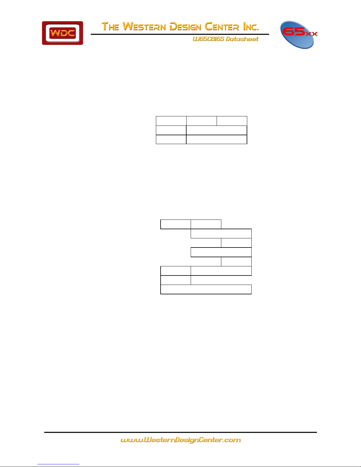
Instruction:
Opcode
dstbnk
srcbnk
Source Address:
srcbnk
X Reg
Dest. Address:
dstbnk
Y Reg
Instruction:
Opcode
offset
Direct Register
+ offset
direct address
+ X Reg
00
(address)
then: +
DBR
Operand Address:
effective address
November 09, 2018
3.5.9 Block Move-xyc
Block Move (xyc) addressing is used by the Block Move instructions. The second byte of the instruction
contains the high-order 8 bits of the destination address and the Y Index Register contains the loworder 16 bits of the destination address. The third byte of the instruction contains the high-order 8 bits
of the source address and the X Index Register contains the low-order bits of the source address. The
C Accumulator contains one less than the number of bytes to move. The second byte of the block
move instructions is also loaded into the Data Bank Register.
Increment X and Y (MVN) or decrement X and Y (MVP) and decrement C (if greater than zero), then
PC=PC+3.
3.5.10 Direct Indexed Indirect-(d,x)
Direct Indexed Indirect ((d,x)) addressing is often referred to as Indirect X addressing. The second byte
of the instruction is added to the sum of the Direct Register and the X Index Register. The result points
to the X low-order 16 bits of the effective address. The Data Bank Register contains the high-order 8
bits of the effective address.
19
Page 20

Instruction:
Opcode
offset
Direct Register
+ offset
direct address
+ X Reg
Operand
Address:
00
effective address
Instruction:
Opcode
offset
Direct Register
+ offset
direct address
+ Y Reg
Operand
Address:
00
effective address
Instruction:
Opcode
offset
Direct Register
+ offset
00
(direct address)
then: +
DBR
base address
+
Y Reg
Operand
Address:
effective address
November 09, 2018
3.5.11 Direct Indexed with X-d,x
With Direct Indexed with X (d,x) addressing the second byte of the instruction is added to the sum of the
Direct Register and the X Index Register to form the 16-bit effective address. The operand is always in
Bank 0.
3.5.12 Direct Indexed with Y-d,y
With Direct Indexed with Y (d,y) addressing the second byte of the instruction is added to the sum of the
Direct Register and the Y Index Register to form the 16-bit effective address. The operand is always in
Bank 0.
3.5.13 Direct Indirect Indexed-(d),y
Direct Indirect Indexed ((d),y) addressing is often referred to as Indirect Y addressing. The second byte
of the instruction is added to the Direct Register (D). The 16-bit content of this memory location is then
combined with the Data Bank register to form a 24-bit base address. The Y Index Register is added to
the base address to form the effective address.
20
Page 21

Instruction:
Opcode
offset
Direct Register
+ offset
00
direct address
base address
then +
Y Reg
Operand
Address:
effective address
Instruction:
Opcode
offset
Direct Register
then:
+ offset
00
(direct address)
Operand
Address:
direct address
Instruction:
Opcode
offset
Direct Register
+ offset
00
(direct address)
then: +
DBR
Operand
Address:
effective address
November 09, 2018
3.5.14 Direct Indirect Long Indexed-[d],y
With Direct Indirect Long Indexed ([d],y) addressing the 24-bit base address is pointed to by the sum
of the second byte of the instruction and the Direct Register. The effective address is this 24-bit base
address plus the Y Index Register.
3.5.15 Direct Indirect Long-[d]
With Direct Indirect Long ([d]) addressing the second byte of the instruction is added to the Direct
Register to form a pointer to the 24-bit effective address.
3.5.16 Direct Indirect-(d)
With Direct Indirect ((d)) addressing the second byte of the instruction is added to the Direct Register to
form a pointer to the low-order 16 bits of the effective address. The Data Bank Register contains the
high-order 8 bits of the effective address.
21
Page 22

Instruction:
Opcode
offset
Direct Register
+
offset
Operand
Address:
00
effective address
November 09, 2018
3.5.17 Direct-d
With Direct (d) addressing the second byte of the instruction is added to the Direct Register (D) to
form the effective address. An additional cycle is required when the Direct Register is not page
aligned (DL not equal 0). The Bank register is always 0.
3.5.18 Immediate-#
With Immediate (#) addressing the operand is the second byte (second and third bytes when in the
16-bit mode) of the instruction.
3.5.19 Implied-i
Implied (i) addressing uses a single byte instruction. The operand is implicitly defined by the instruction.
3.5.20 Program Counter Relative Long-rl
The Program Counter Relative Long (rl) addressing mode is used with only with the unconditional
Branch Long instruction (BRL) and the Push Effective Relative instruction (PER). The second and
third bytes of the instruction are added to the Program Counter, which has been updated to point to
the opcode of the next instruction. With the branch instruction, the Program Counter is loaded with
the result. With the Push Effective Relative instruction, the result is stored on the stack. The offset is
a signed 16-bit quantity in the range from -32768 to 32767. The Program Bank Register is not
affected.
3.5.21 Program Counter Relative-r
The Program Counter Relative (r) addressing is referred to as Relative Addressing and is used only
with the Branch instructions. If the condition being tested is met, the second byte of the instruction is
added to the Program Counter, which has been updated to point to the opcode of the next instruction.
The offset is a signed 8-bit quantity in the range from -128 to 127. The Program Bank Register is not
affected.
3.5.22 Stack-s
Stack (s) addressing refers to all instructions that push or pull data from the stack, such as Push, Pull,
Jump to Subroutine, Return from Subroutine, Interrupts, and Return from Interrupt. The bank address
is always 0. Interrupt Vectors are always fetched from Bank 0.
22
Page 23

Instruction:
Opcode
offset
Stack Pointer
then: +
offset
Operand Address:
00
effective address
Instruction:
Opcode
offset
Stack Pointer
offset
00
S + offset
then +
DBR
base address
+
Y Reg
Operand Address:
effective address
November 09, 2018
3.5.23 Stack Relative-d,s
With Stack Relative (d,s) addressing the low-order 16 bits of the effective address is formed from the
sum of the second byte of the instruction and the stack pointer. The high-order 8 bits of the effective
address are always zero. The relative offset is an unsigned 8-bit quantity in the range of 0 to 255.
3.5.24 Stack Relative Indirect Indexed-(d,s),y
With Stack Relative Indirect Indexed ((d,s),y) addressing the second byte of the instruction is added to
the Stack Pointer to form a pointer to the low-order 16-bit base address in Bank 0. The Data Bank
Register contains the high-order 8 bits of the base address. The effective address is the sum of the 24bit base address and the Y Index Register.
23
Page 24

Address Mode
Instruction Times in Memory
Cycle
Memory Utilization in Number
of Program Sequence Bytes
Original 8-bit
NMOS
6502
New
W65C816S
Original 8-bit
NMOS
6502
New
W65C816S
Absolute
4 (5)
4 (3,5)
3
3
Absolute Indexed Indirect (Jump)
- 6 -
3
Absolute Indirect (Jump)
5 5 3
3
Absolute Long
-
5 (3)
-
4
Absolute Long, X
-
5 (3)
-
4
Absolute, X
4 (1,5)
4 (1,3,5)
3
3
Absolute, Y
4 (1)
4 (1,3)
3
3
Accumulator
2 2 1
1
Block Move (xyc)
- 7 -
3
Direct
3 (5)
3 (3,4,5)
2
2
Direct Indexed Indirect (d,x)
6
6 (3,4)
2
2
Direct Indirect
-
5 (3,4)
-
2
Direct Indirect Indexed (d),y
5 (1)
5 (1,3,4)
2
2
Direct Indirect Indexed Long [d],y
-
6 (3,4)
-
2
Direct Indirect Long
-
6 (3,4)
-
2
Direct, X
4 (5)
4 (3,4,5)
2
2
Direct, Y
4
4 (3,4)
2
2
Immediate
2
2 (3)
2
2 (3)
Implied 2 2 1 1
Relative
2 (1,2)
2 (2)
2
2
Relative Long
-
3 (2)
-
3
Stack
3-7
3-8 1 1
Stack Relative
-
4 (3)
-
2
Stack Relative Indirect Indexed
-
7 (3)
-
2
November 09, 2018
Table 3-1 Addressing Mode Summary
Notes (these are indicated in parentheses):
1. Page boundary, add 1 cycle if page boundary is crossed when forming address. STA
abs,x takes 5 cycles when M=1.
2. Branch taken, add 1 cycle if branch is taken.
3. M = 0 or X = 0, 16 bit operation, add 1 cycle, add 1 byte for immediate.
4. Direct register low (DL) not equal zero, add 1 cycle.
5. Read-Modify-Write, add 2 cycles for M = 1, add 3 cycles for M = 0.
24
Page 25
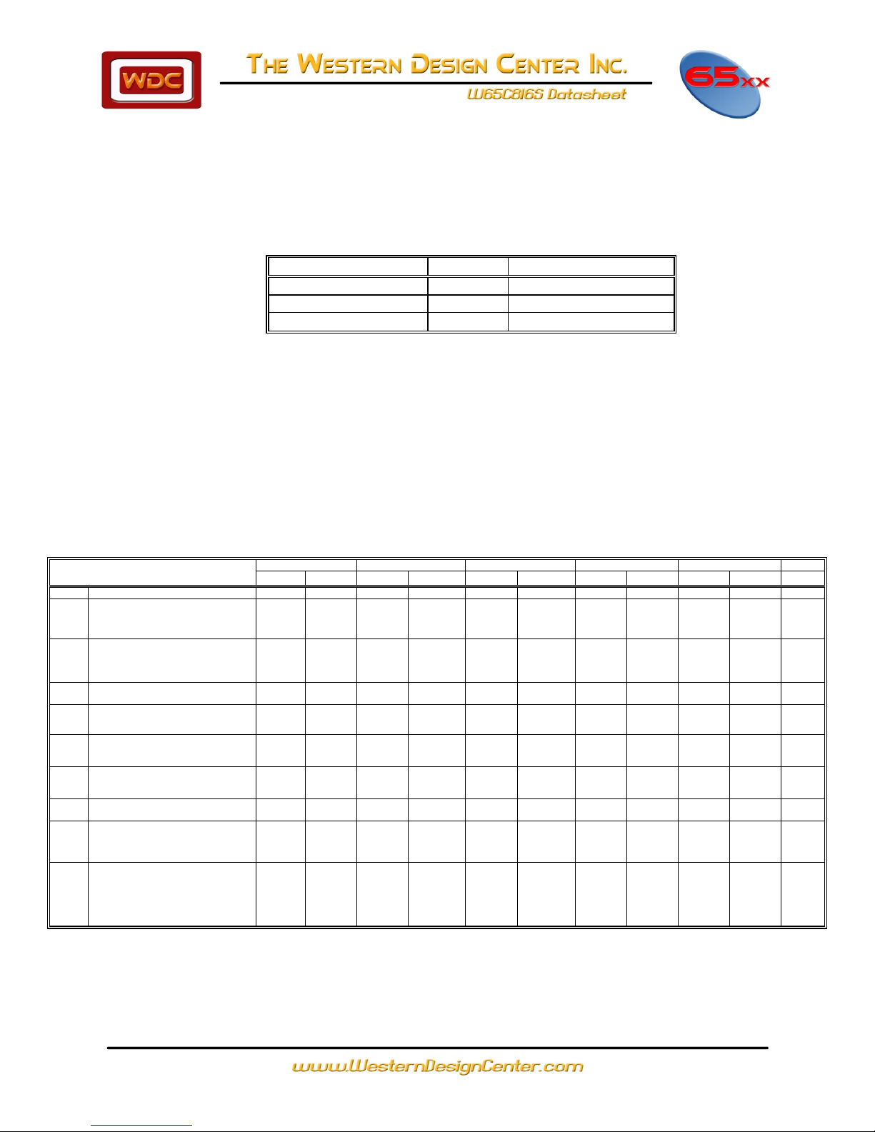
Rating
Symbol
Value
Supply Voltage
VDD
-0.3 to +7.0V
Input Voltage
VIN
-0.3 to VDD +0.3V
Storage Temperature
TS
-55C to +150C
5.0 +/- 5%
3.3 +/- 10%
3.0 +/- 5%
2.5 +/- 5%
1.8 +/- 5%
Units
Min
Max
Min
Max
Min
Max
Min
Max
Min
Max VDD 4.75
5.25
3.0
3.6
2.85
3.15
2.375
2.625
1.71
1.89
V
Vih
Input High Voltage
ABORTB, BE, Data, IRQB, RDY,
NMIB, PHI2, RESB
VDDx0.
8
VDD+0.3
VDDx0.8
VDD+0.3
VDDx0.8
VDD+0.3
VDDx0.8
VDD+0.3
VDDx0.8
VDD+0.3
V
Vil
Input Low Voltage
ABORTB, BE, Data, IRQB, RDY,
NMIB, PHI2, RESB
VSS-
0.3
VDDx0.
2
VSS-0.3
VDDx0.2
VSS-0.3
VDDx0.2
VSS-0.3
VDDx0.
2
VSS-0.3
VDDx0.
2
V
Ipup
RDY Input Pullup-Current
(VIN=VDDx0.8)
5
20 5 20 5 20 2 10 2 10
A
Iin
Input Leakage Current (Vin=0.4 to 2.4)
PHI2, Address, Data, RWB, (Off state,
BE=0), All other inputs
-0.2
0.2
-0.2
0.2
-0.2
0.2
-0.2
0.2
-0.2
0.2
A
Ioh
Output High Voltage (Vol=VDD-0.4V)
Address, Data, E, MLB, MX,
RWB, VDA, VPA, VPB
700 - 300 - 300 - 200 - 100
-
A
Iol
Output Low Voltage (Vol=VSS+0.4V)
Address, Data, E, MLB, MX, RWB,
VDA, VPA, VPB
3.2
20
1.6 - 1.6 - 1.0 - .5 - mA
Idd
Supply Current (no load)
Supply Current (core)
- - 2.0
1.0
-
1.5
0.6
-
1.5
0.5
-
1.0
0.4
-
0.75
0.30
mA/
MHz
Isby
Standby Current (No Load, Data Bus =
VSS or VDD)
ABORTB, BE, IRQB, NMIB, RESB,
PHI2=VDD
- 1 - 1 - 1 -
1
A
Cin
Cts
Capacitance (Vin=0V, TA=25C, f=1MHz)
ABORTB, BE, IRQB, NMIB, PHI2,
RBW, RESB, RDY,
Address, Data, R/W- (Off state)
* Not inspected during production
test; verified on a sample basis.
- 5 - 5 - 5 - 5 -
5
pF
pF
November 09, 2018
4 TIMING, AC AND DC CHARACTERISTICS
4.1 Absolute Maximum Ratings
Table 4-1 Absolute Maximum Ratings
This device contains input protection against damage due to high static voltages or electric fields;
however, precautions should be taken to avoid application of voltages higher than the maximum
rating.
Note: Exceeding these ratings may result in permanent damage. Functional operation under the
conditions is not implied.
4.2 DC Characteristics TA = -40°C to +85°C
Table 4-2 DC Characteristics
25
Page 26

0.0
0.2
0.4
0.6
0.8
1.0
1.2
1.4
1.6
1.8
2.0
2.2
2.4
0 1 2 3 4
5
6
+
+
+
+
IDD (mA)
VDD (VOLTS)
1MHz Operation@85°C
Typical 0.6u processed device
(With tester loading)
(Core power only)
+
0.0
0.5
1.0
1.5
2.0
2.5
3.0
3.5
4.0
4.5
5.0
5.5
6.0
0 4 8
+
+
+
+
VDD (VOLTS)
F Max (MHz)
Typical 0.6µ processed device @85°C
2 6 10 12 14 16 18 20
November 09, 2018
Figure 4-1 IDD vs. VDD
26
Figure 4-2 F Max vs. VDD
Page 27

Symbol
Parameter
5.0 +/- 5%
3.3 +/- 10%
3.0 +/- 5%
2.5 +/- 5%
1.8 +/- 5%
Units
14MHz
8MHz
8MHz
4MHz
2MHz
Min
Max
Min
Max
Min
Max
Min
Max
Min
Max
VDD
4.75
5.25
3.0
3.6
2.85
3.15
2.375
2.675
1.71
1.89
V
tCYC
Cycle Time
70
DC
125
DC
125
DC
250
DC
500
DC
nS
tPWL
Clock Pulse Width Low
35 - 63 - 63 - 125
-
250 - nS
tPWH
Clock Pulse Width High
35 - 62 - 62 - 125
-
250 - nS
tF,tR
Fall Time, Rise Time
-
5 - 5 - 5 - 5 - 5
nS
tAH
A0-A15 Hold Time
10 - 10 - 10 - 20 - 40 - nS
tADS
A0-A15 Setup Time
-
30 - 40 - 40 - 75 - 150
nS
tBH
BA0-BA7 Hold Time
10 - 10 - 10 - 20 - 40 - nS
tBAS
BA0-BA7 Setup Time
-
33 - 40 - 40 - 75 - 150
nS
tACC
Access Time
30 - 70 - 70 - 130
-
365 - nS
tDHR
Read Data Hold Time
10 - 10 - 10 - 20 - 40 - nS
tDSR
Read Data Setup Time
10 - 15 - 20 - 30 - 40 - nS
tMDS
Write Data Delay Time
-
30 - 40 - 40 - 70 - 140
nS
tDHW
Write Data Hold Time
10 - 10 - 10 - 20 - 40 - nS
tPCS
Processor Control Setup
Time
10 - 15 - 15 - 30 - 60 - nS
tPCH
Processor Control Hold
Time
10 - 10 - 10 - 20 - 40 - nS
tEH
E, MX Output Hold Time
-
5 - 5 - 5 - 5 - 5
nS
tES
E, MX Output Setup Time
10 - 15 - 15 - 30 - 60 - nS
CEXT
Capacitive Load (1)
-
35 - 35 - 35 - 35 - 35
Pf
tBVD
be TO Valid Data (2)
-
25 - 30 - 30 - 60 - 120
nS
Table 4-2 W65C816S AC Characteristics
1. Test or loading on all outputs.
2. BE to High Impedance State is not testable but should be the same amount of time as BE to Valid
Data.
27
Page 28

PHI2
tPWL
tCYC
tMDS
tAH
tR
RWB, MLB, VPB
A0-A15, VDA VPA
READ DATA,
BA0-BA7
WRITE DATA,
BA0-BA7
IRQB, NMIB,
RESB, RDY
tF
tPWH
tF
ABORTB
M/X
E
tADS
tBAS
BA0-BA7
BA0-BA7
WRITE DATA
READ DATA
tDSR
tACC
tES
tDHR
tDHW
tPCS
tPCH
M
X X
tPCS
tEH
tES
M
tEH
November 09, 2018
1. Timing measurement points are 50% VDD.
28
Figure 4-1 General Timing Diagram
Page 29
1.
ADC
Add Memory to Accumulator with Carry
47.
PHB
Push Data Bank Register on Stack
2.
AND
"AND" Memory with Accumulator
48.
PHD
Push Direct Register on Stack
3.
ASL
Shift One Bit Left, Memory or Accumulator
49.
PHK
Push Program Bank Register on Stack
4.
BCC
Branch on Carry Clear (C=0)
50.
PHP
Push Processor Status on Stack
5.
BCS
Branch on Carry Set (C=1)
51.
PHX
Push Index X on Stack
6.
BEQ
Branch if Equal (Z=1)
52.
PHY
Push Index Y on Stack
7.
BIT
Bit Test
53.
PLA
Pull Accumulator from Stack
8.
BMI
Branch if Result Minus (N=1)
54.
PLB
Pull Data Bank Register from Stack
9.
BNE
Branch if Not Equal (Z=0)
55.
PLD
Pull Direct Register from Stack
10.
BPL
Branch if Result Plus (N=0)
56.
PLP
Pull Processor Status from Stack
11.
BRA
Branch Always
57.
PLX
Pull Index X from Stack
12.
BRK
Force Break
58.
PLY
Pull Index Y from Stack
13.
BRL
Branch Always Long
59.
REP
Reset Status Bits
14.
BVC
Branch on Overflow Clear (V=0)
60.
ROL
Rotate One Bit Left (Memory or Accumulator)
15.
BVS
Branch on Overflow Set (V=1)
61.
ROR
Rotate One Bit Right
16.
CLC
Clear Carry Flag
62.
RTI
Return from Interrupt
17.
CLD
Clear Decimal Mode
63.
RTL
Return from Subroutine Long
18.
CLI
Clear Interrupt Disable Bit
64.
RTS
Return from Subroutine
19.
CLV
Clear Overflow Flag
65.
SBC
Subtract Memory from Accumulator
20.
CMP
Compare Memory and Accumulator
66.
SEP
Set Processor Status Bit
21.
COP
Coprocessor
67.
SEC
Set Carry Flag
22.
CPX
Compare Memory and Index X
68.
SED
Set Decimal Mode
23.
CPY
Compare Memory and Index Y
69.
SEI
Set Interrupt Disable Status
24.
DEC
Decrement Memory or Accumulator by One
70.
STA
Store Accumulator in Memory
25.
DEX
Decrement Index X by One
71.
STP
Stop the Clock
26.
DEY
Decrement Index Y by One
72.
STX
Store Index X in Memory
27.
EOR
"Exclusive OR" Memory with Accumulator
73.
STY
Store Index Y in Memory
28.
INC
Increment Memory or Accumulator by One
74.
STZ
Store Zero in Memory
29.
INX
Increment Index X by One
75.
TAX
Transfer Accumulator in Index X
30.
INY
Increment Index Y by One
76.
TAY
Transfer Accumulator to Index Y
31.
JML
Jump Long
77.
TCD
Transfer C Accumulator to Direct Register
32.
JMP
Jump to New Location
78.
TCS
Transfer C Accumulator to Stack Pointer
33.
JSL
Jump Subroutine Long
79.
TDC
Transfer Direct Register to C Accumulator
34.
JSR
Jump to News Location Saving Return
80.
TRB
Test and Reset Bit
35.
LDA
Load Accumulator with Memory
81.
TSB
Test and Set Bit
36.
LDX
Load Index X with Memory
82.
TSC
Transfer Stack Pointer to C Accumulator
37.
LDY
Load Index Y with Memory
83.
TSX
Transfer Stack Pointer Register to Index X
38.
LSR
Shift One Bit Right (Memory or Accumulator)
84.
TXA
Transfer Index X to Accumulator
39.
MVN
Block Move Negative
85.
TXS
Transfer Index X to Stack Pointer Register
40.
MVP
Block Move Positive
86.
TXY
Transfer Index X to Index Y
41.
NOP
No Operation
87.
TYA
Transfer Index Y to Accumulator
42.
ORA
"OR" Memory with Accumulator
88.
TYX
Transfer Index Y to Index X
43.
PEA
Push Absolute Address
89.
WAI
Wait for Interrupt
44.
PEI
Push Indirect Address
90.
WDM
Reserved for future use
45.
PER
Push Program Counter Relative Address
91.
XBA
Exchange B and A Accumulator
46.
PHA
Push Accumulator on Stack
92.
XCE
Exchange Carry and Emulation Bits
November 09, 2018
5 OPERATION TABLES
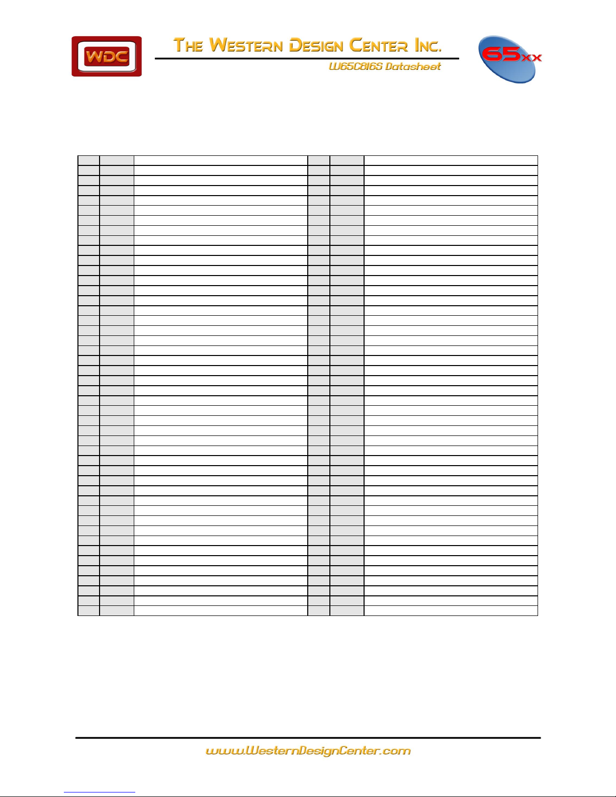
Table 5-1 W65C816S Instruction Set-Alphabetical Sequence
29
Page 30

Address
Label
Function
00FFFE,F
IRQB/BRK
Hardware/Software
00FFFC,D
RESETB
Hardware
00FFFA,B
NMIB
Hardware
00FFF8,9
ABORTB
Hardware
00FFF6,7
(Reserved)
Hardware
00FFF4,5
COP
Software
00FFF2,3
(Reserved)
00FFF0,1
(Reserved)
Address
Label
Function
00FFEE,F
IRQB
Hardware
00FFEC,D
(Reserved)
00FFEA,B
NMIB
Hardware
00FFE8,9
ABORTB
00FFE6,7
BRK
Software
00FFE4,5
COP
Software
00FFE2,3
(Reserved)
00FFE0,1
(Reserved)
November 09, 2018
Table 5-2 Emulation Mode Vector Locations (8-bit Mode)
Table 5-3 Native Mode Vector Locations (16-bit Mode)
The VP output is low during the two cycles used for vector location access. When an interrupt is executed,
D=0 and I=1 in Status Register P.
30
Page 31

M M
S S
D D
0 1 2 3 4 5 6 7 8 9 A B C D E F
BRK ORA COP ORA TSB ORA ASL ORA PHP ORA ASL PHD TSB ORA ASL ORA
s (d,x) s d,s d d d [d] s # A s a a a al
7,2 6,2 7,2 4,2 5,2 3,2 5,2 6,2 3,1 2,2 2,1 4,1 6,3 4,3 6,3 5,4
BPL ORA ORA ORA TRB ORA ASL ORA CLC ORA INC TCS TRB ORA ASL ORA
r (d),y (d) (d,s),y d d,x d,x [d],y i a,y A i a a,x a,x al,x
2,2 5,2 5,2 7,2 5,2 4,2 6,2 6,2 2,1 4,3 2,1 2,1 6,3 4,3 7,3 5,4
JSR AND JSL AND BIT AND ROL AND PLP AND ROL PLD BIT AND ROL AND
a (d,x) al d,s d d d [d] s # A s a a a al
6,3 6,2 8,4 4,2 3,2 3,2 5,2 6,2 4,1 2,2 2,1 5,1 4,3 4,3 6,3 5,4
BMI AND AND AND BIT AND ROL AND SEC AND DEC TSC BIT AND ROL AND
R (d),y (d) (d,s),y d,x d,x d,x [d],y i a,y A i a,x a,x a,x al,x
2,2 5,2 5,2 7,2 4,2 4,2 6,2 6,2 2,1 4,3 2,1 2,1 4,3 4,3 7,3 5,4
RTI EOR WDM EOR MVP EOR LSR EOR PHA EOR LSR PHK JMP EOR LSR EOR
s (d,x) i d,s xyc d d [d] s # A s a a a Al
7,1 6,2 2,2 4,2 7,3 3,2 5,2 6.2 3,1 2,2 2,1 3,1 3,3 4,3 6,3 5,4
BVC EOR EOR EOR MVN EOR LSR EOR CLI EOR PHY TCD JMP EOR LSR EOR
r (d),y (d) (d,s),y xyc d,x d,x [d].y i a,y
s
i al a,x a,x al,x
2,2 5,2 5,2 7,2 7,3 4,2 6,2 6,2 2,1 4,3 3,1 2,1 4,4 4,3 7,3 5,4
RTS ADC PER ADC STZ ADC ROR ADC PLA ADC ROR RTL JMP ADC ROR ADC
s (d,x) s d,s d d d [d] s # A s (a) a a al
6,1 6,2 6,3 4,2 3,2 3,2 5,2 6,2 4,1 2,2 2,1 6,1 5,3 4,3 6,3 5,4
BVS ADC ADC ADC STZ ADC ROR ADC SEI ADC PLY TDC JMP ADC ROR ADC
r (d),y (d) (d,s),y d,x d,x d,x [d],y i a,y s i (a,x) a,x a,x al,x
2,2 5,2 5,2 7,2 4,2 4,2 6,2 6,2 2,1 4,3 4,1 2,1 6,3 4,3 7,3 5,4
BRA STA BRL STA STY STA STX STA DEY BIT TXA PHB STY STA STX STA
r (d,x) rl d,s d d d [d] i # i s a a a al
2,2 6,2 4,3 4,2 3,2 3,2 3,2 2,2 2,1 2,2 2,1 3,1 4,3 4,3 4,3 5,4
BCC STA STA STA STY STA STX STA TYA STA TXS TXY STZ STA STZ STA
r (d),y (d) (d,s),y d,x d,x d,y [d],y i a,y i i a a,x a,x al,x
2,2 6,2 5,2 7,2 4,2 4,2 4,2 6,2 2,1 5,3 2,1 2,1 4,3 5,3 5,3 5,4
LDY LDA LDX LDA LDY LDA LDX LDA TAY LDA TAX PLB LDY LDA LDX LDA
# (d,x) # d,s d d d [d] i # i s a a a al
2,2 6,2 2,2 4,2 3,2 3,2 3,2 6,2 2,1 2,2 2,1 4,1 4,3 4.3 4,3 5,4
BCS LDA LDA LDA LDY LDA LDX LDA CLV LDA TSX TYX LDY LDA LDX LDA
r (d),y (d) (d,s),y d,x d,x d,y [d],y i a,y i i a,x a,x a,y al,x
2.2 5,2 5,2 7,2
4,2 4,2 4,2
6,2 2,1 4,3
2,1 2,1 4,3 4,3 4,3 5,4
CPY CMP REP CMP CPY CMP DEC CMP INY CMP DEX WAI CPY CMP CMP
# (d,x) # d,s d d d [d] i # i I a a al
2,2 6,2 3,2 4,2 3,2 3,2 5,2 6,2 2,1 2,2 2,1 3,1 4,3 4,3 6,3 5,4
BNE CMP CMP CMP PEI CMP DEC CMP CLD CMP PHX STP JML CMP DEC CMP
r (d),y (d) (d,s),y s d,x d,x [d],y i a,y s i (a) a,x a,x al,x
2,2 5,2 5,2 7,2 6,2 4,2 6,2 6,2 2,1 4,3 3,1 3,1 6,3 4,3 7,3 5,4
CPX SBC SEP SBC CPX SBC INC SBC INX SBC NOP XBA CPX SBC INC SBC
# (d,x) # d,s d d d [d] i # i i a a a al
2,2 6,2 3,2 4,2 3,2 3,2 5,2 6,2 2,1 2,2 2,1 3,1 4,3 4,3 6,3 5,4
BEQ SBC SBC PEA SBC INC SBC SED SBC PLX XCE JSR SBC INC SBC
r (d) (d,s),y s d,x d,x [d],y i a,y s i (a,x) a,x a,x al,x
2,2 5,2 5,2 7,2 5,3 4,2 6,2 6,2 2,1 4,3 4,1 2,1 8,3 4,3 7.3 5,4
0 1 2 3 4 5 6 7 8 9 A B C D E F
New OPCODE on the W65C816S
OPCODE with new features on the W65C816S
Cycle Count Assumes:
-- branches are not taken
-- no page boundary crossings (if in emulation mode)
-- the M and X flags are 1 (8-bit Accumulator and Index Registers)
-- BRK and COP assume emulation mode
-- RTI assumes native mode
SBC (d),y
FEE
F
DEC a
B
D
C
C
D
B
A99A678678345
345
2
2
LSD
0
0
1
1
November 09, 2018
Table 5-4 Opcode Matrix
31
Page 32

Mnemonic
Operation
Opcodes
Status Register
7 6 5 4 3 2 1 0 Addressing Mode
a
A
a,x
a,y
al
al,x
(a)
(a,x)
d
d,s
d,x
d,y
(d)
[d]
(d,s),
y
(d,x)
(d),y
[d],y
i
r
rl
s
xyc
#
N V M X D I Z
C
1 2 3 4 5 6 7 8 9
10
11
12
13
14
15
16
17
18
19
20
21
22
23
24 N V 1 B D I Z C
ADC
A+M+CA
6D 7D
79
6F
7F
65
63
75 72
67
73
61
71
77 69 N V . . . . Z C
AND
A^MA
2D 3E
39
2F
3F
25
23
35 32
27
33
21
31
37 29 N . . . . . Z .
ASL
C15/7 6 … 10 0
0E
0A
1E 06 16 N . . . . . Z
C
BCC
Branch if C = 0
90 . . . . . . . .
BCS
Branch if C = 1
B0 . . . . . . . .
BEQ
Branch if Z = 1
F0 . . . . . . . .
BIT
A ^ M (Note 1)
2C 3C 24 34
89
M M
. . . . Z
.
BMI
Branch if N = 0
30 . . . . . . . .
BNE
Branch if Z = 0
D0 . . . . . . . .
BPL
Branch if N = 0
10 . . . . . . . .
BRA
Branch Always
80 . . . . . . . .
BRK
Break (Note 2)
00 . . . • 0 1 . .
BRL*
Branch Long Always
82 . . . . . . .
.
BVC
Branch if V = 0
50 . . . . . . . .
BVS
Branch if V = 1
70 . . . . . . . .
CLC
C 0
18 . . . . . . .
0
CLD
0 D
D8 . . . . 0 . .
.
CLI
0 1
58 . . . . . 0 .
.
CLV
0 V
B8 . 0 . . . . .
.
CMP
A-M
CD DD
D9
CF
DF
C5
C3
D5 D2
C7
D3
C1
D1
D7 C9 N . . . . . Z C
COP*
Co-Processor
02 . . . . 0 1 . .
CPX
X-M
EC E4
E0
N . . . . . Z
C
CPY
Y-M
CC C4
C0
N . . . . . Z
C
DEC
Decrement
CE
3A
DE C6 D6
N . . . . . Z
.
DEX
X-1 A
CA
N . . . . . Z
.
DEY
Y-1 Y
88
N . . . . . Z
.
EOR
A xv M A
4D 5D
59
4F
5F 5D
45
43
55 52
47
53
41
51
57 49
N . . . . . Z
.
INC
Increments
EE
1A
FE E6 F6
N . . . . . Z
.
INX
X+1 X
E8
N . . . . . Z
.
INY
Y+1 Y
C8
N . . . . . Z
.
JML*
Jump Long to new
location
DC
. . . . . . .
.
JMP
Jump to new location
4C 5C 6C
7C
. . . . . . .
.
JSL*
Jump long to
subroutine
22
. . . . . . .
.
JSR
Jump to Subroutine
20
FC
. . . . . . .
.
LDA
M A
AD BD
B9
AF
BF
A5
A3
B5 B2
A7
B3
A1
B1
B7 A9
N . . . . . Z
.
November 09, 2018
Table 5-5 Operation, Operation Codes, and Status Register
32
Page 33

Mnemonic
Operation
OpCodes
Status Register
Addressing Mode
7 6 5 4 3 2 1
0
a
A
a,x
a,y
al
al,x
(a)
(a,x)
d
d,s
d,x
d,y
(d)
[d]
(d,s),
y
(d,x)
(d),y
[d],y
i
r
rl
s
xyc
#
N V M X D I Z
C
1 2 3 4 5 6 7 8 9
10
11
12
13
14
15
16
17
18
19
20
21
22
23
24 N V 1 B D I Z C
LDX
M X
AE
BE
A6
B6 A2 N . . . . . Z .
LDY
M Y
AC BC A4 B4
A0 N . . . . .
Z
.
LSR
0 15/7 6 … 1 0 C
4E
4A
5E 46 56 0 . . . . . Z C MVN*
MM NEGATIVE
54 . . . . . . .
.
MVP*
MM POSITIVE
44 . . . . . . .
.
NOP
No Operation
EA . . . . . . .
.
ORA
A V M A
0D 1D
19
0F
1F
05
03
15 12
07
13
01
11
17 09 N . . . . .
Z
.
PEA*
Mpc+1, Mpc+2 → Ms-1, Ms
S-2 → S
F4 . . . . . . . .
PEI*
M(d), M(d+1) → Ms-1, Ms
S-2 → S
D4 . . . . . . . .
PER*
Mpc+rl, Mpc+rl+1 → Ms-1,
Ms S-2 → S
62 . . . . . . . .
PHA
A Ms, S-1 S
48 . . . . . . . .
PHB*
DBR → Ms, S-1 → S
8B . . . . . . . .
PHD*
D → Ms, Ms-1, S-2 → S
0B . . . . . . . .
PHK*
PBR → Ms, S-1 → S
4B . . . . . . . .
PHP
P Ms, S-1 S
08 . . . . . . . .
PHX
X Ms, S-1 S
DA . . . . . . . .
PHY
Y Ms, S-1 S
5A . . . . . . . .
PLA
S + 1 S, Ms A
68 N . . . . . Z .
PLB
S + 1 S, Ms DBR
AB N . . . . . Z .
PLD
S + 2 S, Ms – 1, Ms
→ D
2B N . . . . . Z .
PLP
S + 1 S, Ms P
28 N V M X D 1 Z C
PLX
S + 1 S, Ms X
FA N . . . . . Z .
PLY
S + 1 S, Ms Y
7A N . . . . . Z
REP
M^P P
C2 N V M X D 1 Z C
ROL
C 15/7 6 5 4 3 2 1 0
C
2E
2A
3E 26 36 N . . . . . Z
C
ROR
C 15/7 6 5 4 3 2 1 0
C
6E
6A
7E 66 76 N . . . . . Z
C
RTI
Return from Interrupt
40 N V M X D 1 Z C
RTL*
Return from Sub.
Long
6B . . . . . . . .
RTS
Return from
Subroutine
60 . . . . . . . .
SBC
A – M – (C) A
ED FD
F9 FF
E5
E3
F5 F2
E7
F3
E1
F1
F7 E9 N V . . . . Z C
SEC
1 C
38 . . . . . . .
1
SED
1 D
F8 . . . . 1 . .
.
SEI
1 1
78 . . . . . 1 .
.
SEP*
MVP P
E2
N V M X D 1 Z
C
STA
A M
8D 9D 8F
9F
85
83
95 92
87
93
81
91
97
. . . . . . . . STP
STOP (1 PH12)
D8
. . . . . . .
.
STX
X M
8E 86
96
. . . . . . .
.
November 09, 2018
Table 5-5 continued
33
Page 34
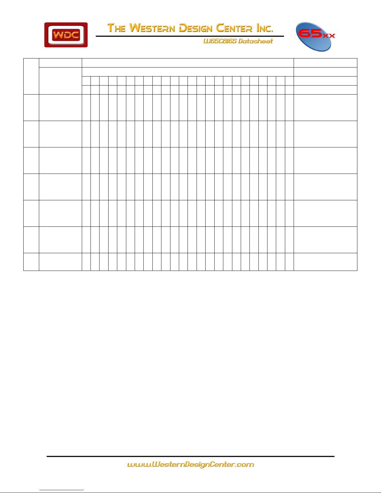
Mnemonic
Operation
OpCodes
Status Register
7 6 5 4 3 2 1 0 Addressing Mode
a
A
a,x
a,y
al
al,x
(a)
(a,x)
d
d,s
d,x
d,y
(d)
[d]
(d,s),
y
(d,x)
(d),y
[d],y
i
r
rl
s
xyc
#
N V M X D I Z
C
1 2 3 4 5 6 7 8 9 10
11
12
13
14
15
16
17
18
19
20
21
22
23
24 N V 1 B D I Z C
STY
Y M
8C 84 94 . . . . . . .
.
STZ
00 M
9C 9E 64 74 . . . . . . .
.
TAX
A X
AA N . . . . . Z
.
TAY
A Y
AB N . . . . . Z
.
TCD*
C D
5B N . . . . . Z
.
TCS*
C S
1B . . . . . . .
.
TDC*
D C
7B N . . . . . Z
.
TRB
1C 14 . . . . . . Z
.
TSB
AVM M
0C 04 . . . . . . Z
.
TSC*
S C
3B N . . . . .
Z
.
TSX
S X
BA N . . . . .
Z
.
TXA
X A
8A N . . . . .
Z
.
TXS
X S
9A , . . . . .
,
.
TXY*
X Y
9B N . . . . .
Z
.
TYA
Y A
98 N . . . . .
Z
TYX*
Y X
BB N . . . . .
Z
.
WAI
0 RDY
CB . . . . . .
.
.
WDM*
No Operation
42 . . . . . .
.
.
XBA*
B A
EB N . . . . .
Z
.
XCE*
M Y
FB . . . . . .
.
E
November 09, 2018
Table 5-5 continued
Notes:
1) The following are the definitions of the operational symbols used:
+ ADD, ^ AND, xv Exclusive OR, * Multiply, ~ NOT, v OR, - Subtract
2) Bit immediate N and V flags not affected. When M=0, M15N and M14V.
3) Break Bit (B) in Status register indicates hardware or software break.
4) = New W65C816 instructions
34
Page 35

Symbol
Addressing Mode
Symbol
Addressing Mode
#
immediate
[d]
direct indirect long
A
accumulator
[d],y
direct indirect long indexed
r
program counter relative
a
absolute
rl
program counter relative long
a,x
absolute indexed with x
I
implied
a,y
absolute indexed with y
s
stack
al
absolute long
d
direct
al,x
absolute long indexed
d,x
direct indexed with x
d,s
stack relative
d,y
direct indexed with y
(d,s),y
stack relative indirect indexed
(d)
direct indirect
(a)
absolute indirect
(d,x)
direct indexed indirect
(a,x)
absolute indexed indirect
(d),y
direct indirect indexed
xyc
block move
November 09, 2018
Table 5-6 Addressing Mode Symbol Table
35
Page 36

Address Mode
Note
Cycle VPB
MLB
VDA
(14)
VPA
(14)
Address Bus
(15)
Data Bus
RWB
1a. Absolute a
ADC, AND, BIT, CMP, CPX, CPY, EOR,
LDA, LDX LDY ORA, SBC, STA, STX,
STY, STZ,
18 OpCodes, 3 bytes, 4 & 5 cycles
(1)
1
2
3
4
4a
1
1
1
1
1
1
1
1
1
1
1
0
0
1
1
1
1
1
0
0
PBR,PC
PBR,PC+1
PBR,PC+2
DBR,AA
DBR,AA+1
OpCode
AAL
AAH
Data Low
Data High
1
1
1
1/0
1/0
1b. Absolute a
JMP (4C)
1 OpCode, 3 bytes, 3 cycles
1
2
3
1
1
1
1
1
1
1
1
1
1
0
0
1
1
1
1
1
PBR,PC
PBR,PC+1
PBR,PC+2
PBR,New PC
OpCode
New PCL
New PCH
OpCode
1
1
1
1
1c. Absolute a
JSR
1 OpCode, 3 bytes, 6 cycles
(different order from N6502)
1
2
3
4
5
6
1
1
1
1
1
1
1
1
1
1
1
1
1
1
1
1
0
0
0
1
1
1
1
1
1
0
0
0
1
PBR,PC
PBR,PC+1
PBR,PC+2
PBR,PC+2
0,S
0,S-1
PBR,NEWPC
OpCode
New PCL
New PCH
IO
PCH
PCL
Next
OpCode
1
1
1
1
0
0
1
1d. Absolute (R-M-W) a
ASL, DEC, INC, LSR, ROL, ROR, TRB,
TSB
6 OpCodes, 3 bytes, 6 & 8 cycles
(1)
(3)(17)
(1)
1
2
3
4
4a
5
6a
6
1
1
1
1
1
1
1
1
1
1
1
0
0
0
0
0
1
0
0
1
1
0
1
1
1
1
1
0
0
0
0
0
PBR,PC
PBR,PC+1
PBR,PC+2
DBR,AA
DBR,AA+1
DBR,AA+1
DBR,AA+1
DBR,AA
OpCode
AAL
AAH
Data Low
Data High
IO
Data High
Data Low
1
1
1
1
1
1
0
0
2a. Absolute Indexed Indirect (a,x)
JMP
1 OpCode, 3 bytes, 6 cycles
1
2
3
4
5
6
1
1
1
1
1
1
1
1
1
1
1
1
1
1
1
1
0
0
0
0
0
1
1
1
1
0
1
1
1
PBR,PC
PBR-PC+1
PBR-PC+2
PBR,PC+2
PBR,AA+X
PBR,AA+X+1
PBR,NEW PC
OpCode
AAL
AAH
IO
New PCL
New PCH
OpCode
1
1
1
1
1
1
1
2b. Absolute Indexed Indirect (a,x)
JSR
1 OpCode, 3 bytes, 8 cycles
1
2
3
4
5
6
7
8
1
1
1
1
1
1
1
1
1
1
1
1
1
1
1
1
1
1
1
1
0
1
1
0
0
0
0
1
1
1
0
0
1
0
1
1
1
PBR,PC
PBR,PC+1
0,S
0,S-1
PBR,PC+2
PBR,PC+2
PBR,AA+X
PBR,AA+X+1
PBR,NEW PC
OpCode
AAL
PCH
PCL
AAH
IO
New PCL
New PCH
Next
OpCode
1
1
0
0
1
1
1
1
1
3a. Absolute Indirect (a)
JML
1 OpCode, 3 bytes, 6 cycles
1
2
3
4
5
6
1
1
1
1
1
1
1
1
1
1
1
1
1
1
1
1
0
0
1
1
1
1
1
1
1
0
0
0
1
PBR,PC
PBR,PC+1
PBR,PC+2
0,AA
0,AA+1
0,AA+2
NEW PBR,PC
OpCode
AAL
AAH
New PCL
New PCH
New PBR
OpCode
1
1
1
1
1
1
1
3b. Absolute Indirect (a)
JMP
1 OpCode, 3 bytes, 5 cycles
1
2
3
4
5
1
1
1
1
1
1
1
1
1
1
1
1
1
1
0
0
1
1
1
1
1
1
0
0
1
PBR,PC
PBR,PC+1
PBR,PC+2
0,AA
0,AA+1
PBR,NEW PC
OpCode
AAL
AAH
New PCL
New PCH
OpCode
1
1
1
1
1
1
November 09, 2018
Table 5-7 Instruction Operation (continued on following 6 pages)
36
Page 37

Address Mode
Note
Cycle VPB
MLB
VDA
(14)
VPA
(14)
Address Bus (15)
Data Bus
RWB
4a. Absolute Long al
ADC, AND, CMP, EOR, LDA, ORA,
SBC, STA, 8 OpCodes, 4 bytes,
5 & 6 cycles
(1)
1
2
3
4
5
5a
1
1
1
1
1
1
1
1
1
1
1
1
1
0
0
0
1
1
1
1
1
1
0
0
PBR,PC
PBR,PC+1
PBR,PC+2
PBR,PC+3
AAB,AA
AAB,AA+1
OpCode
AAL
AAH
AAB
Data Low
Data High
1
1
1
1
1/0
1/0
4b. Absolute Long (JUMP) al
JMP
1 OpCode, 4 bytes, 4 cycles
1
2
3
4
1
1
1
1
1
1
1
1
1
1
1
1
0
0
0
1
1
1
1
1
1
PBR,PC
PBR,PC+1
PBR,PC+2
PBR,PC+3
New PBR,PC
OpCode
New PCL
New PCH
New BR
OpCode
1
1
1
1
1
4c. Absolute Long (JUMP to Subroutine
Long) al
JSL
1 OpCode, 4 bytes, 8 cycles
1
2
3
4
5
6
7
8
1
1
1
1
1
1
1
1
1
1
1
1
1
1
1
1
1
1
1
1
0
0
1
0
0
1
1
1
1
1
1
0
0
1
0
0
1
PBR,PC
PBR,PC+1
PBR,PC+2
0,S
0,S
PBR,PC+3
0,S-1
0,S-2
New PBR,PC
OpCode
New PCL
New PCH
PBR
IO
New PBR
PCH
PCL
Next OpCode
1
1
1
0
1
1
0
0
1
5. Absolute Long,X al,x
ADC, AND, CMP, EOR, LDA, ORA,
SBC, STA
8 OpCodes, 4 bytes, 5 and 6 cycles
(1)
1
2
3
4
5
5a
1
1
1
1
1
1
1
1
1
1
1
1
1
0
0
0
1
1
1
1
1
1
0
0
PBR,PC
PBR,PC+1
PBR,PC+2
PBR,PC+3
AAB,AA+X
AAB,AA+X+1
OpCode
AAL
AAH
AAB
Data Low
Data High
1
1
1
1
1/0
1/0
6a Absolute, X a, x
ADC, AND, BIT, CMP, EOR, LDA, LDY,
ORA, SBC, STA, STZ
12 OpCodes, 3 bytes, 4,5 and 6 cycles
(4)
(1)
1
2
3
3a
4
4a
1
1
1
1
1
1
1
1
1
1
1
1
1
0
0
0
1
1
1
1
1
0
0
0
PBR,PC
PBR,PC+1
PBR,PC+2
DBR,AAH,AAL+XL
DBR,AA+X
DBR,AA+X+1
OpCode
AAL
AAH
IO
Data Low
Data High
1
1
1
1
1/0
1/0
6b Absolute, X(R-M-W) a,x
ASL, DEC INC LSR ROL, ROR
6 OpCodes, 3 bytes, 7 and 9 cycles
(1)
(3)(17)
(1)
1
2
3
4
5
5a
6
7a
7
1
1
1
1
1
1
1
1
1
1
1
1
1
0
0
0
0
0
1
0
0
0
1
1
0
1
1
1
1
1
0
0
0
0
0
0
PBR,PC
PBR,PC+1
PBR,PC+2
DBR,AAH,AAL+XL
DBR,AA+X
DBR,AA+X+1
DBR,AA+X+1
DBR,AA+X+1
DBR,AA+X
OpCode
AAL
AAH
IO
Data Low
Date High
IO
Data High
Data Low
1
1
1
1
1
1
1
0
0
7. Absolute, Y a,y
ADC, AND, CMP, EOR, LDA, LDX,
ORA, SBC, STA
9 OpCodes, 3 bytes, 4,5 and 6 cycles
(4)
(1)
1
2
3
3a
4
4a
1
1
1
1
1
1
1
1
1
1
1
1
1
0
0
0
1
1
1
1
1
0
0
0
PBR,PC
PBR,PC+1
PBR,PC+2
DBR,AAH,AAL+YL
DBR,AA+Y
DBR,AA+Y+1
OpCode
AAL
AAH
IO
Data Low
Data High
1
1
1
1
1/0
1/0
8. Accumulator A
ASL, DEC, INC, LSR, ROL, ROR
6 OpCodes, 1 byte, 2 cycles
1
2
1
1
1
1
1
0
1
0
PBR,PC
PBR,PC+1
OpCode
IO 1 1
November 09, 2018
Table 5-7 (continued)
37
Page 38

Address Mode
Note
Cycle
VPB
MLB
VDA
(14)
VPA
(14)
Address Bus
(15)
Data Bus
RWB
9a. Block Move Negative
(backward) xyc
MVN
1 Op Code N-2
3 bytes Byte
7 cycles C=2
x=Source Address
y=Destination
c=# of bytes to move-1
x,y Increment
N Byte
C=0
1
2
3
4
5
6
7
1
2
3
4
5
6
7
1
2
3
4
5
6
7
1
1
1
1
1
1
1
1
1
1
1
1
1
1
1
1
1
1
1
1
1
1
1
1
1
1
1
1
1
1
1
1
1
1
1
1
1
1
1
1
1
1
1
1
1
1
0
0
1
1
0
0
1
0
0
1
1
0
0
1
0
0
1
1
0
0
1
1
1
1
0
0
0
0
1
1
1
0
0
0
0
1
1
1
0
0
0
0
1
PBR,PC
PBR,PC+1
PBR,PC+2
SBA,X
DBA,Y
DBA,Y
DBA,Y
PBR,PC
PBR,PC+1
PBR,PC+2
SBA,X+1
DBA,Y+1
DBA,Y+1
DBA,Y+1
PBR,PC
PBR,PC+1
PBR,PC+2
SBA,X+2
DBA,Y+2
DBA,Y+2
DBA,Y+2
PBR,PC+3
OpCode
DBA
SBA
SRC Data
Dest Data
IO
IO
OpCode
DBA
SBA
SRC Data
Dest Data
IO
IO
OpCode
DBA
SBA
SRC Data
Dest Data
IO
IO
Next
OpCode
1
1
1
1
0
1
1
1
1
1
1
0
1
1
1
1
1
1
0
1
1
1
9b. Block Move Positive
(forward) xyc
(MVP)
1 Op Code N-2
3 bytes Byte
7 cycles C=2
x=Source Address
y=Destination
c=# of bytes to move-1
x,y Decrement
MVP is used when the destination
N-1
start address is higher (more
Byte
positive ) than the source
C=1
start address.
N Byte
Last
C=0
000000
1
2
3
4
5
6
7
1
2
3
4
5
6
7
1
2
3
4
5
6
7
1
1
1
1
1
1
1
1
1
1
1
1
1
1
1
1
1
1
1
1
1
1
1
1
1
1
1
1
1
1
1
1
1
1
1
1
1
1
1
1
1
1
1
1
1
1
0
0
1
1
0
0
1
0
0
1
1
0
0
1
0
0
1
1
0
0
1
1
1
1
0
0
0
0
1
1
1
0
0
0
0
1
1
1
0
0
0
0
1
PBR,PC
PBR,PC+1
PBR,PC+2
SBA,X
DBA,Y
DBA,Y
DBA,Y
PBR,PC
PBR,PC+1
PBR,PC+2
SBA,X-1
DBA,Y-1
DBA,Y-1
DBA,Y-1
PBR,PC
PBR,PC+1
PBR,PC+2
SBA,X-2
DBA,Y-2
DBA,Y-2
DBA,Y-2
PBR,PC+3
OpCode
DBA
SBA
SRC Data
Dest Data
IO
IO
OpCode
DBA
SBA
SRC Data
Dest Data
IO
IO
OP Code
DBA
SBA
SRC Data
Dest Data
IO
IO
Next
OpCode
1
1
1
1
0
1
1
1
1
1
1
0
1
1
1
1
1
1
0
1
1
1
Source End
Dest. End
Source
Start
Destination.
Start
Source Start
Destination.
FFFFF
000000
FFFFFF
November 09, 2018
Table 5-7 (continued)
38
Page 39

Address Mode
Note
Cycle
VPB
MLB
VDA
(14)
VPA
(14)
Address Bus (15)
Data Bus
RWB
10a. Direct d
ADC AND BIT, CMP, CPX, CPY ,EOR,
LDA, LDX, LDY, ORA, SBC, STA, STX,
STY, STZ
16 OpCodes, 2 bytes, 3, 4 & 5 cycles
(2)
(1)
1
2
2a
3
3a
1
1
1
1
1
1
1
1
1
1
1
0
0
1
1
1
1
0
0
0
PBR,PC
PBR,PC+1
PBR,PC+1
0,D+DO
0,D+DO+1
OpCode
DO
IO
Data Low
Data High
1
1
1
1/0
1/0
10b. Direct (R-M-W)d
ASL, DEC, INC, LSR, ROL, ROR, TRB,
TSB,
8 OpCodes, 2 bytes, 5,6,7 and 8 cycles
(2)
(1)
(3),(17)
(1)
1
2
2a
3
3a
4
5a
5
1
1
1
1
1
1
1
1
1
1
1
0
0
0
0
0
1
0
0
1
1
0
1
1
1
1
0
0
0
0
0
0
PBR, PC
PBR,PC+1
PBR,PC+1
0,D+DO
0,D+DO+1
0,D+DO+1
0,D+DO+1
0,D+DO
OpCode
DO
IO
Data Low
Data High
IO
Data High
Data Low
1
1
1
1
1
1
0
0
11. Direct Indexed Indirect (d,x)
ADC, AND, CMP, EOR, LDA, ORA,
SBC, STA,
8 OpCodes, 2 bytes, 6,7 and 8 cycles
(2)
(1)
1
2
2a
3
4
5
6
6a
1
1
1
1
1
1
1
1
1
1
1
1
1
1
1
1
1
0
0
0
1
1
1
1
1
1
0
0
0
0
0
0
PBR,PC
PBR,PC+1
PBR,PC+1
PBR,PC+1
0,D+DO+X
0,D+DO+X+1
DBR,AA
DBR,AA+1
OpCode
DO
IO
IO
AAL
AAH
Data Low
Data High
1
1
1
1
1
1
1/0
1/0
12. Direct Indirect (d)
ADC, AND, CMP, EOR, LDA, ORA,
SBC. STA,
8 OpCodes 2 bytes, 5,6 and 7 cycles
(2)
(1)
1
2
2a
3
4
5
5a
1
1
1
1
1
1
1
1
1
1
1
1
1
1
1
0
0
1
1
1
1
1
1
0
0
0
0
0
PBR,PC
PBR,PC+1
PBR,PC+1
0,D+DO
0,D+DO+1
DBR,AA
DBR,AA+1
OpCode
DO
IO
AAL
AAH
Data Low
Data High
1
1
1
1
1
1/0
1/0
13. Direct Indirect Indexed (d),y
ADC, AND, CMP, EOR, LDA, ORA,
SBC, STA
8 OpCodes, 2 bytes, 5,6,7 and 8 cycles
(2)
(4)
(1)
1
2
2a
3
4
4a
5
5a
1
1
1
1
1
1
1
1
1
1
1
1
1
1
1
1
1
0
0
1
1
0
1
1
1
1
0
0
0
0
0
0
PBR,PC
PBR,PC+1
PBR,PC+1
0,D+DO
0,D+DO+1
DBR,AAH.AAL+YL
DBR,AA+Y
DBR,AA+Y+1
OpCode
DO
IO
AAL
AAH
IO
Data Low
Data High
1
1
1
1
1
1
1/0
1/0
14. Direct Indirect Indexed Long [d],y
ADC, AND, CMP, EOR, LDA, ORA, SBC,
STA
8 OpCodes, 2 bytes, 6,7 and 8 cycles
(2)
(1)
1
2
2a
3
4
5
6
6a
1
1
1
1
1
1
1
1
1
1
1
1
1
1
1
1
1
0
0
1
1
1
1
1
1
1
0
0
0
0
0
0
PBR,PC
PBR,PC+1
PBR,PC+1
0,D+DO
0,D+DO+1
0,D+DO+2
AAB,AA+Y
AAB,AA+Y+1
OpCode
DO
IO
AAL
AAH
AAB
Data Low
Data High
1
1
1
1
1
1
1/0
1/0
15. Direct Indirect Long [d]
ADC, AND, CMP, EOR, LDA, ORA,
SBC, STA
8 OpCodes, 2 bytes, 6,7 and 8 cycles
(2)
(1)
1
2
2a
3
4
5
6
6a
1
1
1
1
1
1
1
1
1
1
1
1
1
1
1
1
1
0
0
1
1
1
1
1
1
1
0
0
0
0
0
0
PBR,PC
PBR,PC+1
PBR,PC+1
0,D+DO
0,D+D0+1
0,D+DO+2
AAB,AA
AAB,AA+1
OpCode
DO
IO
AAL
AAH
AAB
Data Low
Data High
1
1
1
1
1
1
1/0
1/0
November 09, 2018
Table 5-7 (continued)
39
Page 40

Address Mode
Note
Cycle
VPB
MLB
VDA
(14)
VPA
(14)
Address Bus
(15)
Data Bus
RWB
16a. Direct, X d,x
ADC, AND, BIT, CMP, EOR, LDA
LDY, ORA, SBC, STA, STY, STZ,
12 OpCodes,2 bytes, 4,5,and 6
cycles
(2)
(1)
1
2
2a
3
4
4a
1
1
1
1
1
1
1
1
1
1
1
1
1
0
0
0
1
1
1
1
0
0
0
0
PBR,PC
PBR,PC+1
PBR,PC+1
PBR,PC+1
0,D+DO+X
0,D+DO+X+1
OpCode
DO
IO
IO
Data Low
Data High
1
1
1
1
1/0
1/0
16b. Direct, X (R-M-W) d,x
ASL, DEC, INC, LSR, ROL, ROR,
6 OpCodes, 2 bytes, 6,7,8 and 9
cycles
(2)
(1)
(3),(17
)
(1)
1
2
2a
3
4
4a
5
6a
6
1
1
1
1
1
1
1
1
1
1
1
1
1
0
0
0
0
0
1
0
0
0
1
1
0
1
1
1
1
0
0
0
0
0
0
0
PBR,PC
PBR,PC+1
PBR,PC+1
PBR,PC+1
0,D+DO+X
0,D+DO+X+1
0,D+DO+X+1
0,D+DO+X+1
0,D+DO+X
OpCode
DO
IO
IO
Data Low
Data High
IO
Data High
Data Low
1
1
1
1
1
1
1
0
0
17. Direct, Y d,y
LDX, STX
2 OpCodes, 2 bytes, 4,5 and 6
cycles
(2)
(1)
1
2
2a
3
4
4a
1
1
1
1
1
1
1
1
1
1
1
1
1
0
0
0
1
1
1
1
0
0
0
0
PBR,PC
PBR,PC+1
PBR,PC+1
PBR,PC+1
0,D+DO+Y
0,D+DO+Y+1
OpCode
DO
IO
IO
Data Low
Data High
1
1
1
1
1/0
1/0
18.Immediate #
ADC, AND, BIT, CMP, CPX, CPY,
EOR, LDA, LDX, LDY, ORA, REP,
SEC, SEP
14 OpCodes, 2 and 3 bytes, 2 and
3 cycles
(1)(8)
1
2
2a
1
1
1
1
1
1
1
0
0
1
1
1
PBR,PC
PBR,PC+1
PBR,PC+2
OpCode
IDL
IDH
1
1
1
19a. Implied i
CLC, CLD, CLI, CLV, DEX, DEY,
INX, INY, NOP, SEC, SED, SEI,
TAX, TAY, TCD, TCS, TDC, TSC,
TSX, TXA, TXS, TXY, TYA, TYX,
XCE
25 OpCodes, 1 byte, 2 cycles
1
2
1
1
1
1
1
0
1
0
PBR,PC
PBR,PC+1
OpCode
IO
1
1
19b. Implied i
XBA
1 OpCode, 1 byte, 3 cycles
1
2
3
1
1
1
1
1
1
1
0
0
1
0
0
PBR,PC
PBR,PC+1
PBR,PC+1
OpCode
IO
IO
1
1
1
19c. Stop the Clock
STP
1 OpCode
1 byte RESB=1
3 cycles RESB=0
RESB=0
RESB=1
(See 22a. Stack Hardware
Interrupt)
1
2
3
1c
1b
1a
1
1
1
1
1
1
1
1
1
1
1
1
1
1
1
1
0
0
0
0
0
1
1
0
0
0
0
0
1
PBR,PC
PBR,PC+1
PBR,PC+1
PBR,PC+1
PBR,PC+1
PBR,PC+1
PBR,PC+1
OpCode
IO
IO
RES (BRK)
RES (BRK)
RES (BRK)
BEGIN
1
1
1
1
1
1
1
19d. Wait for Interrupt
WAI
1 OpCode,1 byte
3 cycles IRQB, NMIB
RDY=1
(9)RDY=1
RDY=0
RDY=1
1
2
3
1
1
1
1
1
1
1
1
1
1
0
0
1
1
0
0
1
PBR,PC
PBR,PC+1
PBR,PC+1
PBR,PC+1
OpCode
IO
IO
IRQ(BRK)
1
1
1
1
November 09, 2018
Table 5-7 (continued)
40
Page 41

Address Mode
Note
Cycle
VPB
MLB
VDA
(14)
VPA
(14)
Address Bus
(15)
Data Bus
RWB
20. Relative r
BCC, BCS, BEQ, BMI, BNE, BPL, BRA,
BVC,BVS
9 OpCodes, 2 bytes, 2,3 and 4 cycles
(5)
(6)
1
2
2a
2b
1
1
1
1
1
1
1
1
1
1
1
1
0
0
0
1
1
1
0
0
1
PBR,PC
PBR,PC+1
PBR,PC+1
PBR,PC+1
PBR,PC+Offset
OpCode
Offset
IO
IO
OpCode
1
1
1
1
1
21. Relative Long rl
BRL
1 OpCode, 3 bytes, 4 cycles
1
2
3
4
1
1
1
1
1
1
1
1
1
1
1
1
0
0
0
1
1
1
1
0
1
PBR,PC
PBR,PC+1
PBR,PC+2
PBR,PC+2
PBR,PC+Offset
OpCode
Offset Low
Offset High
IO
OpCode
1
1
1
1
1
22a. Stack s
ABORT, IRQ, NMI, RES
4 hardware interrupts
0 bytes, 7 and 8 cycles
(3)
(7)
(10)
(10)
(10)
(11)
1
2
3
4
5
6
7
8
1
1
1
1
1
1
1
0
0
1
1
1
1
1
1
1
1
1
1
1
0
1
1
1
1
1
1
1
1
0
0
0
0
0
0
0
1
PBR,PC
PBR,PC
0,S
0,S-1
0,S-2
0.S-3
0,VA
0,VA+1
0,AAV
IO
IO
PBR
PCH
PCL
P
AAVL
AAVH
Next OpCode
1
1
0
0
0
0
1
1
1
22b. Stack s
PLA, PLB, PLD, PLP, PLX, PLY
Different than N6502
6 Op Codes,1 byte, 4 and 5 cycles
(1)
1
2
3
4
4a
1
1
1
1
1
1
1
1
1
1
1
0
0
1
1
1
0
0
0
0
PBR,PC
PBR,PC+1
PBR,PC+1
0,S+1
0,S+2
OpCode
IO
IO
REG Low
REG High
1
1
1
1
1
22c. Stack s
PHA, PHB PHP, PHD, PHK, PHX, PHY
7 Op Codes, 1 byte, 3 and 4 cycles
(1)
(12)
1
2
3a
3
1
1
1
1
1
1
1
1
1
0
1
1
1
0
0
0
PBR,PC
PBR,PC+1
0,S
0,S-1
OpCode
IO
REG High
REG Low
1
1
0
0
22d. Stack s
PEA
1 Op Code, 3 bytes, 5 cycles
1
2
3
4
5
1
1
1
1
1
1
1
1
1
1
1
0
0
1
1
1
1
1
0
0
PBR,PC
PBR,PC+1
PBR,PC+2
0,S
0,S-1
OpCode
AAL
AAH
AAH
AAL
1
1
1
0
0
22e. Stack s
PEI
1 Op Code, 2 bytes, 6 and 7 cycles
(2)
1
2
2a
3
4
5
6
1
1
1
1
1
1
1
1
1
1
1
1
1
1
1
0
0
1
1
1
1
1
1
0
0
0
0
0
PBR,PC
PBR,PC+1
PBR,PC+1
0,D+DO
0,D+DO+1
0,S
0,S-1
OpCode
DO
IO
AAL
AAH
AAH
AAL
1
1
1
1
1
0
0
22f. Stack s
PER
1 Op Code, 3 bytes, 6 cycles
1
2
3
4
5
6
1
1
1
1
1
1
1
1
1
1
1
1
1
0
0
0
1
1
1
1
1
0
0
0
PBR,PC
PBR,PC+1
PBR,PC+2
PBR,PC+2
0,S
0,S-1
OpCode
Offset Low
Offset High
IO
PCH+Offset+Carry
PCL+Offset
1
1
1
1
0
0
November 09, 2018
Table 5-7 (continued)
41
Page 42

Address Mode
Note
Cycle
VPB
MLB
VDA
(14)
VPA
(14)
Address Bus
(15)
Data Bus
RWB
22g. Stack s
RTI
1 Op Code, 1 byte, 6 and 7 cycles
(different order fromN6502)
(3)
(7)
1
2
3
4
5
6
7
1
1
1
1
1
1
1
1
1
1
1
1
1
1
1
1
1
1
0
0
1
1
1
1
1
1
0
0
0
0
0
0
1
PBR,PC
PBR,PC+1
PBR,PC+1
0,S+1
0,S+2
0,S+3
0,S+4
PBR,New PC
OpCode
IO
IO
P
New PCL
New PCH
PBR
Next
OpCode
1
1
1
1
1
1
1
1
22h. Stack s
RTS
1 OpCode, 1 byte, 6 cycles
1
2
3
4
5
6
1
1
1
1
1
1
1
1
1
1
1
1
1
1
1
1
0
0
1
1
0
1
1
0
0
0
0
0
1
PBR,PC
PBR,PC+1
PBR,PC+1
0,S+1
0,S+2
0,S+2
PBR,PC
OpCode
IO
IO
PCL
PCH
IO
OpCode
1
1
1
1
1
1
1
22i. Stack s
RTL
1 Op Code, 1 byte, 6 cycles
1
2
3
4
5
6
1
1
1
1
1
1
1
1
1
1
1
1
1
1
1
1
0
0
1
1
1
1
1
0
0
0
0
0
1
PBR,PC
PBR,PC+1
PBR,PC+1
0,S+1
0,S+2
0,S+3
NEW PBR,PC
OpCode
IO
IO
New PCL
New PCH
New PBR
Next
OpCode
1
1
1
1
1
1
1
22j. Stack s
BRK,COP
2 OpCodes, 2 bytes
7 and 8 cycles
(3)
(7)
(10)
(10)
(10)
1
2
3
4
5
6
7
8
1
1
1
1
1
1
1
0
0
1
1
1
1
1
1
1
1
1
1
1
0
1
1
1
1
1
1
1
1
1
0
0
0
0
0
0
1
PBR,PC
PBR,PC+1
0,S
0,S-1
0,S-2
0,S-3 (16)
0,VA
0,VA+1
0,AAV
OpCode
Signature
PBR
PCH
PCL
P
AAVL
AAVH
Next
OpCode
1
1
0
0
0
0
1
1
1
23. Stack Relative d,s
ADC, AND, CMP, EOR,
LDA, ORA, SBC, STA
8 Op Codes, 2 bytes, 4 and 5 cycles
(1)
1
2
3
4
4a
1
1
1
1
1
1
1
1
1
1
1
0
0
1
1
1
1
0
0
0
PBR,PC
PBR,PC+1
PBR,PC+1
0,S+SO
0,S+SO+1
OpCode
SO
IO
Data Low
Data High
1
1
1
1/0
1/0
24. Stack Relative Indirect Indexed (d,s),y
ADC, AND, CMP, EOR, LDA, ORA, SBC,
STA
8 Op Codes, 2 bytes, 7 and 8 cycles
(1)
1
2
3
4
5
6
7
7a
1
1
1
1
1
1
1
1
1
1
1
1
1
1
1
1
1
0
0
1
1
0
1
1
1
1
0
0
0
0
0
0
PBR,PC
PBR,PC+1
PBR,PC+1
0,S+SO
0,S+SO+1
0,S+SO+1
DBR,AA+Y
DBR,AA+Y+1
OpCode
SO
IO
AAL
AAH
IO
Data Low
Data High
1
1
1
1
1
1
1/0
1/0
November 09, 2018
Table 5-7 (continued)
42
Page 43

November 09, 2018
Notes: Be aware that notes #4-7, 9 and 10 apply to the W65C02S and W65C816S. All other notes apply to the
W65C816S only.
1. Add 1 byte (for immediate only) for M=0 or X=0 (i.e. 16-bit data), add 1 cycle for M=0 or X=0. REP, SEP are
always 3 cycle instructions and VPA is low during the third cycle. The address bus is PC+1 during the third
cycle.
2. Add 1 cycle for direct register low (DL) not equal 0.
3. Special case for aborting instruction. This is the last cycle which may be aborted or the Status, PBR or
DBRregisters will be updated.
4. Add 1 cycle for indexing across page boundaries, or write, or X=0. When X=1 or in the emulation mode, this
cycle contains invalid addresses.
5. Add 1 cycle if branch is taken.
6. Add 1 cycle if branch is taken across page boundaries in 6502 emulation mode (E=1).
7. Subtract 1 cycle for 6502 emulation mode (E=1).
8. Add 1 cycle for REP, SEP.
9. Wait at cycle 2 for 2 cycles after NMIB or IRQB active input.
10. RWB remains high during Reset.
11. BRK bit 4 equals "0" in Emulation mode.
12. PHP and PLP.
13. Some OpCodes shown are compatible only with the W65C816S.
14. VDA and VPA are not valid outputs on the W65C02S but are valid on the W65C816S. The two signals,
VDA and VPA, are included to point out the upward compatibility to the W65C816S. When VDA and VPA
are both a one level, this is equivalent to SYNC being a one level.
15. The PBR is only applicable to the W65C816S.
16. COP Latches.
17. In the emulation mode, during a R-M-W instruction the RWB is low during both write and modify cycles.
43
Page 44

Clock
Bank Address
BA0-BA7
E
D
Q
OE
573 or 373
8
8
Data Bus
D0-D7
8
PHI2
D0-D7
BA0-BA7
R/WB
W65C816S
CE
B
DIR
A
74x245
November 09, 2018
Figure 5-1 Bank Address Latching Circuit
44
Page 45

November 09, 2018
6 RECOMMENDED W65C816S ASSEMBLER SYNTAX STANDARDS
6.1 Directives
Assembler directives are those parts of the assembly language source program which give directions to the
assembler; this includes the definition of data area and constants within a program. This standard excludes
any definitions of assembler directives.
6.2 Comments
An assembler should provide a way to use any line of the source program as a comment. The
recommended way of doing this is to treat any blank line, or any line that starts with a semi-colon or an
asterisk as a comment. Other special characters may be used as well.
6.3 The Source Line
Any line which causes the generation of a single W65C816S machine language instruction should be
divided into four fields: a label field, the operation code, the operand, the comment field.
6.3.1 The Label Field
The label field begins in column one of the line. A label must start with an alphabetic character, and
may be followed by zero or more alphanumeric characters. An assembler may define an upper limit
on the number of characters that can be in a label, so long as that upper limit is greater than or equal
to six characters. An assembler may limit the alphabetic characters to upper-case characters if
desired. If lower-case characters are allowed, they should be treated as identical to their upper-case
equivalents. Other characters may be allowed in the label, so long as their use does not conflict with
the coding of operand fields.
6.3.2 The Operation Code Field
The operation code shall consist of a three character sequence (mnemonic) from Table 7-1. It shall
start no sooner than column 2 of the line, or one space after the label if a label is coded.
6.3.2.1 Many of the operation codes in Table 6-1 have duplicate mnemonics; when two or more
machine language instruction has the same mnemonic, the assembler resolves the difference
based on the operand.
6.3.2.2 If an assembler allows lower-case letters in labels, it must also allow lower-case letters in
the mnemonic. When lower-case letters are used in the mnemonic, they shall be treated as
equivalent to the upper-case counterpart. Thus, the mnemonics LDA, lda and LdA must all be
recognized, and are equivalent.
6.3.2.3 In addition to the mnemonics shown in Table 7-1, an assembler may provide the
alternate mnemonics shown in Table 7-1.
45
Page 46

WDC
Standard
Alias
BCC
BLT
BCS
BGE
CMP A
CMA
DEC A
DEA
INC A
INA
JSL
JSR
JML
JMP
TCD
TAD
TCS
TAS
TDC
TDA
TSC
TSA
XBA
SWA
November 09, 2018
Table 6-1 Alternate Mnemonics
6.3.2.4 JSL should be recognized as equivalent to JSR when it is specified with a long absolute
address forced. JML is equivalent to JMP with long addressing forced.
6.3.3 The Operand Field
The operand field may start no sooner than one space after the operation code field. The
assembler must be capable of at least twenty-four bit address calculations. The assembler should be
capable of specifying addresses as labels, integer constants, and hexadecimal constants. The
assembler must allow addition and subtraction in the operand field. Labels shall be recognized by the
fact they start with alphabetic characters. Decimal numbers shall be recognized as containing only
the decimal digits 0...9. Hexadecimal constants shall be recognized by prefixing the constant with a
"$" character, followed by zero or more of either the decimal digits or the hexadecimal digits "A"..."F".
If lower-case letters are allowed in the label field, then they shall also be allowed as hexadecimal
digits.
6.3.3.1 All constants, no matter what their format, shall provide at least enough precision to
specify all values that can be represented by a twenty-four bit signed or unsigned integer
represented in two's complement notation.
6.3.3.2 Table 7-2 shows the operand formats that shall be recognized by the assembler. bol d is a
label or value which the assembler can recognize as being less than $100. The symbol a is a label
or value which the assembler can recognize as greater than $FF but less than $10000; the symbol
al is a label or value that the assembler can recognize as being greater than $FFF. The symbol
EXT is a label which cannot be located by the assembler at the time the instruction is assembled.
Unless instructed otherwise, an assembler shall assume that EXT labels are two bytes long. The
symbols r and rl are 8 and 16-bit signed displacements calculated by the assembler.
46
Page 47

November 09, 2018
Table 6-2 Address Mode Formats
Addressing Mode Format Addressing Mode Format
Immediate #d Absolute Indexed by Y !d,y
#a d,y
#al a,y
#EXT !a,y
#<d !al,y
#<a !EXT,y
#<al EXT,y
#<EXT Absolute Long Indexed by X >d,x
#>d >a,x
#>a >al,x
#>al al,x
#>EXT >EXT,x
#^d Program Counter Relative d
#^a and Program Counter a
#^al Relative Long al
#^EXT (EXT)
Absolute !d Absolute Indirect (d)
!a (!d)
a (a)
!al (!a)
!EXT (!al)
EXT EXT
Absolute Long >d Direct Indirect (d)
>a (<a)
>al (<al)
al (<EXT)
>EXT Direct Indirect Long [d]
Direct Page d [>a]
<d [>al]
<a [>EXT]
<al Absolute Indexed (d,x)
<EXT (!d,x)
Accumulator A (a,x)
Implied Addressing (no operand) (!a,x)
Direct Indirect (d),y (!al,x)
Indexed (<d,y) (EXT,x)
(<a),y (!EXT,x)
(<al),y Stack Addressing (no operand)
(<EXT),y
Direct Indirect [d],y Stack Relative (d,s),y
Indexed Long [<d],y Indirect Indexed (<d,s),y
[<a],y (<a,s),y
[<al],y (<al,s),y
[<EXT],y (<EXT,s),y
Direct Indexed (d,x) Block Move d,d
Indirect (<d,x) d,a
(<a,x) d,al
(<al,x) d,EXT
(<EXT,x) a,d
Direct Indexed by X d,x a,a
<d,x a,al
<a,x a,EXT
<al,x al,d
<EXT,x al,a
Direct Indexed by Y d,y al,al
<d,y al,EXT
<a,y EXT,d
<al,y EXT,a
<EXT,y EXT,al
Absolute Indexed by X d,x EXT,EXT
!d,x
a,x
!a,x
!al,x
!EXT,x
EXT,x
Note: The alternate ! (exclamation point) is used in place of the | (vertical bar).
47
Page 48
Operand
One Byte
Result
Two Byte
Result
#$01020304
04
04
03
#<$01020304
04
04
03
#>$01020304
03
03
02
#^$01020304
02
02
01
November 09, 2018
6.3.3.3 Note that the operand does not determine whether or not immediate address loads one
or two bytes, this is determined by the setting of the status register. This forces the requirement
for a directive or directives that tell the assembler to generate one or two bytes of space for
immediate loads. The directives provided shall allow separate settings for the accumulator and
index registers.
6.3.3.4 The assembler shall use the <, >, and ^ characters after the # character in immediate
address to specify which byte or bytes will be selected from the value of the operand. Any
calculations in the operand must be performed before the byte selection takes place. Table 7-3
defines the action taken by each operand by showing the effect of the operator on an address.
The column that shows a two byte immediate value show the bytes in the order in which they
appear in memory. The coding of the operand is for an assembler which uses 32-bit address
calculations, showing the way that the address should be reduced to a 24-bit value.
Table 6-3 Byte Selection Operator
6.3.3.5 In any location in an operand where an address, or expression resulting in an address, can
be coded, the assembler shall recognize the prefix characters <, |, and >, which force one byte
(direct page), two byte (absolute) or three byte (long absolute) addressing. In cases where the
addressing modes is not forced, the assembler shall assume that the address is two bytes unless
the assembler is able to determine the type of addressing required by context, in which case that
addressing mode will be used. Addresses shall be truncated without error in an addressing mode is
forced which does not require the entire value of the address. For example, LDA $0203 and LDA
|$010203 are completely equivalent. If the addressing mode is not forced, and the type of
addressing cannot be determined from context, the assembler shall assume that a two byte
address is to be used. If an instruction does not have a short addressing mode (as in LDA< which
has no direct page indexed by Y) and a short address is used in the operand, the assembler shall
automatically extend the address by padding the most significant bytes with zeroes in order to
extend the address to the length needed. As with immediate address, any expression evaluation
shall take place before the address is selected; thus, the address selection character is only used
once, before the address of expression.
6.3.3.6 The (!) exclamation point character should be supported as an alternative to the |
(vertical bar).
6.3.3.7 A long indirect address is indicated in the operand field of an instruction field of an
instruction by surrounding the direct page address where the indirect address is found by square
brackets; direct page addresses which contain 16-bit addresses are indicated by being
surrounded by parentheses.
6.3.4 Comment Field
The comment field may start no sooner than one space after the operation code field or
operand field depending on instruction type.
48
Page 49

Compatibility Issue
NMOS 6502
W65C02
W65C02S
W65C816S
S (Stack)
Always Page 1, 8
bits
Always Page 1, 8
bits
Always page 1, 8
bits
Always page 1 8 bits
when(E=1), 16 bits
when E=0
X (X Index Reg)
Always Page 0
Always less than
256 ie 8 Bits
Always Page 0
Always less than
256 ie 8 Bits
Always Page 0
Always less than
256 ie 8 Bits
Indexed page zero
always in page 0
(E=1), Cross page
(E=0)
Y (Y Index Reg)
Always Page 0
Always less than
256 ie 8 Bits
Always Page 0
Always less than
256 ie 8 Bits
Always Page 0
Always less than
256 ie 8 Bits
Indexed page zero
always in page 0
(E=1), Cross page
(E=0)
A (Accumulator)
8 bits
8 bits
8 bits
8 bits (M=1), 16 bits
(M=0)
(Flag Reg)
N, V and Z flags
invalid in decimal
mode.
D=unknown after
reset. D not modified
after interrupt
N,V and Z flags valid
in decimal mode. D=0
after reset/interrupt
N,V and Z flags valid
in decimal mode. D=0
after reset/interrupt
N,V and Z flags valid in
decimal mode. D=0 after
reset/interrupt
Timing
A.ABS,X,ASL,LSR,
ROL
with no Page
Crossing
B. Jump Indirect
Operand =XXFF
C. Branch Across
Page
D. Decimal Mode
7 cycles
5 cycles and
invalid page
crossing
4 cycles
No add. cycles
6 cycles
6 cycles
4 cycles
Add 1 cycle
6 cycles
6 cycles
4 cycles
Add 1 Cycle
7 cycles
5 cycles
4 cycles
No add. cycles
BRK Vector
FFFE,F BRK bit=0 on
stack if IRQ, NMI
FFFE,F BRK bit=0 on
stack if IRQ, NMI
FFFE,F BRK bit=0 on
stack if IRQ, NMI
00FFFE,F(E=1) BRK
bit=0 on stack if IRQNMIB, ABORTB
000FFE6,7 (E=0), X=X on
stack always
Interrupt or Break
Bank Address
Not available
Not available
Not available
PBR not pushed (E=1)
RTI, PBR, not pulled
(E-1) PRB pushed (E=0)
RTI, PBR pulled (E=0)
Memory Lock (ML)
Not available
MLB=0 during
Modify and Write
cycles
MLB=0 during
Modify and Write
cycles
MLB=0 during Read
Modify and Write
cycles
Indexed Across
Page Boundary
(d),y a,x a,y
Extra read of
invalid address
Extra read of last
instruction fetch
Extra read of last
instruction fetch
Extra read of invalid
address
RDY Pulled during
Write Cycle
Ignored
Processor stops
Processor stops
Processor Stops
November 09, 2018
7 Caveats
Table 7-1 Caveats
49
Page 50

November 09, 2018
7.1 Stack Addressing
When in the Native mode, the Stack may use memory locations 000000 to 00FFFF. The effective address
of Stack, Stack Relative, and Stack Relative Indirect Indexed addressing modes will always be within this
range. In the Emulation mode, the Stack address range is 000100 to 0001FF. The following opcodes and
addressing modes will increment or decrement beyond this range when accessing two or three bytes: JSL,
JSR (a,x), PEA, PEI, PER, PHD, PLD, RTL
7.2 Direct Addressing
7.2.1 The Direct Addressing modes are often used to access memory registers and pointers.
The effective address generated by Direct; Direct,X and Direct,Y addressing modes will always be
in the Native mode range 000000 to 00FFFF. When in the Emulation mode and DL equals zero,
the direct addressing range is 000000 to 0000FF, except for [Direct] and [Direct],Y addressing
modes and the PEI instruction which will increment from 0000FE or 0000FF into the Stack area.
7.2.2 When in the Emulation mode, DH is not equal to zero, and DL is equal to zero, the direct
addressing range is 00DH00 to 00DHFF, except for [Direct] and [Direct],Y addressing modes and
the PEI instruction which will increment from 00DHFE or 00DHFF into the next higher page.
7.2.3 When in the Emulation mode and DL is not equal to zero, the direct addressing range is
000000 to 00FFFF.
7.3 Absolute Indexed Addressing
The Absolute Indexed addressing modes are used to address data outside the direct addressing range.
The W65C02S addressing range is 0000 to FFFF. Indexing from page FFXX may result in a 00YY data
fetch when using the W65C02S. In contrast, indexing from page ZZFFXX may result in ZZ+1,00YY when
using the W65C816S.
7.4 ABORTB Input
7.4.1 ABORTB should be held low for a period not to exceed one cycle. Also, if ABORTB is held
low during the Abort Interrupt sequence, the Abort Interrupt will be aborted. It is not recommended
to abort the Abort Interrupt. The ABORTB internal latch is cleared during the second cycle of the
Abort Interrupt. Asserting the ABORTB input after the following instruction cycles will cause
registers to be modified:
7.4.1.1 Read-Modify-Write: Processor status modified if ABORTB is asserted after a modify cycle.
7.4.1.2 RTI: Processor status modified if ABORTB is asserted after cycle 3.
7.4.1.3 IRQB, NMIB, ABORTB BRK, COP: When ABORTB is asserted after cycle 2, PBR and
DBR will become 00 (Emulation mode) or PBR will become 00 (Native mode).
7.4.2 The ABORT Interrupt has been designed for virtual memory systems. For this reason,
asynchronous ABORTB's may cause undesirable results due to the above conditions
7.5 VDA and VPA Valid Memory Address Output Signals
When VDA or VPA are high and during all write cycles, the Address Bus is always valid. VDA and VPA
should be used to qualify all memory cycles. Note that when VDA and VPA are both low, invalid addresses
may be generated. The Page and Bank addresses could also be invalid. This will be due to low byte
addition only. The cycle when only low byte addition occurs is an optional cycle for instructions which read
memory when the Index Register consists of 8 bits. This optional cycle becomes a standard cycle for the
Store instruction, all instructions using the 16-bit Index Register mode, and the Read-Modify-Write
instruction when using 8- or 16-bit Index Register modes.
50
Page 51

November 09, 2018
7.6 DB/BA operation when RDY is Pulled Low
When RDY is low, the Data Bus is held in the data transfer state (i.e. PHI2 high). The Bank address
external transparent latch should be latched on the rising edge of the PHI2 clock.
7.7 MX Output
The MX output reflects the value of the M and X bits of the processor Status Register. The REP, SEP and
PLP instructions may change the state of the M and X bits. Note that the MX output is invalid during the
instruction cycle following REP, SEP and PLP instruction execution. This cycle is used as the opcode fetch
cycle of the next instruction.
7.8 All Opcodes Function in All Modes of Operation
7.8.1 It should be noted that all opcodes function in all modes of operation. However, some
instructions and addressing modes are intended for W65C816S 24-bit addressing, and are therefore less
useful for the emulation mode. The JSL, RTL, JMP al and JML instructions and addressing modes are
primarily intended for W65C816S native mode use.
7.8.2 The following instructions may be used with the emulation mode even though all Bank
Addresses are forced to $00: PHK, PHB and PLB
7.8.3 The following instructions have "limited" use in the Emulation mode:
7.8.3.1 The REP and SEP instructions cannot modify the M and X bits when in the Emulation
mode. In this mode the M and X bits will always be high (logic 1).
7.8.3.2 MVP and MVN instructions use the X and Y Index Registers for the memory addresses.
When in emulation mode the Source and Destination Bank addresses for MVP and MVN can only move
data in the range 0000 to 00FF. See Programming the 65816 Manual for more information.
7.9 Indirect Jumps
The JMP (a) and JML (a) instructions use the direct Bank for indirect addressing, while JMP (a,x) and JSR
(a,x) use the Program Bank for indirect address tables.
7.10 Switching Modes
When switching from the Native mode to the Emulation mode, the X and M bits of the Status Register are
set high (logic 1), the high byte of the Stack is set to 01, and the high bytes of the X and Y Index
Registers are set to 00. To save previous values, these bytes must always be stored before changing
modes. Note that the low byte of the S, X and Y Registers and the low and high byte of the Accumulator
(A and B) are not affected by a mode change.
7.11 How Interrupts Affect the Program Bank and the Data Bank Registers
7.11.1 When in the Native mode, the Program Bank register (PBR) is cleared to 00 when a
hardware interrupt, BRK or COP is executed. In the Native mode, previous PBR contents are automatically
saved on Stack.
7.11.2 In Emulation Mode the PBR register is cleared to 00 when a hardware interrupt, BRK or
COP is executed. In this case, previous contents of the PBR are not automatically saved.
7.11.3 Note that a Return from Interrupt (RTI) should always be executed from the same "mode"
which originally generated the interrupt.
51
Page 52

November 09, 2018
7.12 Binary Mode
The Binary Mode is set whenever a hardware or software interrupt is executed. The D flag within the Status
Register is cleared to zero.
7.13 Wait for Interrupt (WAI) Instruction
The WAI instruction pulls RDY low and places the processor in the WAI "low power" mode. NMIB, IRQB or
RESB will terminate the WAI condition and transfer control to the interrupt handler routine. Note that an
ABORTB input will abort the WAI instruction, but will not restart the processor. When the Status Register I
flag is set (IRQB disabled) the IRQB interrupt will cause the next instruction (following the WAI instruction) to
be executed without going to the IRQB interrupt handler. This method results in the highest speed response
to an IRQB input. When an interrupt is received after an ABORTB which occurs during the WAI instruction,
the processor will return to the WAI instruction. Other than RESB (highest priority), ABORTB is the next
highest priority, followed by NMIB or IRQB interrupts.
7.14 Stop-the-Clock (STP) Instruction
The STP instruction disables the PHI2 clock to all internal circuitry. When disabled, the PHI2 clock is held in
the high state. In this case, the Data Bus will remain in the data transfer state and the Bank address will not
be multiplexed onto the Data Bus. Upon executing the STP instruction, the RESB signal is the only input
which can restart the processor. The processor is restarted by enabling the PHI2 clock, which occurs on the
falling edge of the RESB input. Note that the external oscillator must be stable and operating properly
before RESB goes high.
7.15 Co-Processor (COP) Signatures
Signatures 00-7F may be user defined, while signatures 80-FF are reserved for instructions on future
microprocessors. Contact WDC for software emulation of future microprocessor hardware functions.
7.16 WDM Opcode Use
The WDM opcode may be used on future microprocessors. It performs no operation. WDM are the initials
of William D. Mensch, Jr., the founder of WDC.
7.17 RDY Pulled During Write
The NMOS 6502 does not stop during a write operation. In contrast, both the W65C02S and the
W65C816S do stop during write operations
7.18 MVN and MVP Affects on the Data Bank Register
The MVN and MVP instructions change the Data Bank Register to the value of the second byte of the
instruction (destination bank address).
52
Page 53

LONGA
ON
REP
#$20
LDA
#$2345
STA
MIKE
LONGA
OFF
SEP
#$20
LDA
#$01
STA
SAM
LONGA
ON
REP
#$20
STA
BOB
November 09, 2018
7.19 Interrupt Priorities
The following interrupt priorities will be in effect should more than one interrupt occur at the same time:
Priority
Highest Priority 1. RESB
Lower 2. Abortb’
Lower 3 NMIB
Lowest 4 IRQB
7.20 Transfers from 8-Bit to 16-Bit, or 16-Bit to 8-Bit Registers
All transfers from one register to another will result in a full 16-bit output from the source register. The
destination register size will determine the number of bits actually stored in the destination register and the
values stored in the processor Status Register. The following are always 16-bit transfers, regardless of the
accumulator size: TCS, TSC, TCD and TDC
Note: PHP and PLP are always 8 bit operations.
7.21 Stack Transfers
When in the Emulation mode, a 01 is forced into SH. In this case, the B Accumulator will not be loaded into
SH during a TCS instruction. When in the Native mode, the B Accumulator is transferred to SH. Note that
in both the Emulation and Native modes, the full 16 bits of the Stack Register are transferred to the A, B and
C Accumulators, regardless of the state of the M bit in the Status Register.
7.22 BRK Instruction
The BRK instruction for the NMOS 6502, 65C02 and 65C816 is actually a 2 byte instruction. The NMOS
device simply skips the second byte (i.e. doesn’t care about the second byte) by incrementing the program
counter twice. The 65C02 and 65C816 does the same thing except the assembler is looking for the second
byte as a “signature byte”. With either device (NMOS or CMOS), the second byte is not used. It is
important to realize that if a return from interrupt is used it will return to the location after the second or
signature byte.
7.23 Accumulator switching from 8-bit to 16-bit
Care must be taken when switching from 16-bit mode to 8-bit mode then to 16-bit mode. The B register is
restored so that the following code shows a potential problem:
Here BOB = $2301 and NOT $000V
53
Page 54

November 09, 2018
8 HARD CORE MODEL
8.1 W65C816 Core Information
The W65C816S core uses the same instruction set as the W65C816S
The only functional difference between the W65C816S and W65C816S core is the RDY pin. The
W65C816S RDY pin is bi-directional utilizing an active pull-up. The W65C816S core RDY
function is split into 2 pins, RDYIN and WAITN. The WAITN output goes low when a WAI
instruction is executed.
The W65C816S core will be a smaller die since the I/O buffers have been removed.
The outputs are the N-channel and P-channel output transistors drivers.
The following inputs, if not used, must be held in the high state: RDY input, IRQB, MIB, BE and
ABORTB.
The timing of the W65C816S core is the same as the W65C816S.
9 SOFT CORE RTL MODEL
9.1 W65C816 Synthesizable RTL-Code in Verilog HDL
The RTL-Code (Register Transfer Level) in Verilog is a synthesizable model. The behavior of this model is
equivalent to the original W65C816S hard core. The W65C816S RTL-Code is available as the core model
and the W65C816S standard chip model. The standard chip model includes the soft core and the buffer
ring in RTL-Code. Synthesizable cores are useful in ASIC design.
54
Page 55

Example: W65C816S6TPLG-14
Description
W65C
W65C = standard product
Product Identification Number
816S
Foundry Process
6T
6=.6u 1P/2M CMOS Process
T= TSMC Foundry
Package
PL
P = Plastic Dual-In-Line, 40 pins
PL = Plastic Leaded Chip Carrier, 44 pins
Q = Quad Flat Pack, 44 pins
RoHS/Green Compliance
G
G = RoHS/Green Compliant (Wafer and Packaging)
Temperature/Processing
-40°C to + 85°C
Speed Designator
-14
-14 = 14MHz
November 09, 2018
10 ORDERING INFORMATION
To receive general sales or technical support on standard product or information about our module library
licenses, contact us at:
The Western Design Center, Inc.
2166 East Brown Road
Mesa, Arizona 85213 USA
Phone: 480-962-4545 Fax: 480-835-6442
www.WDC65xx.com
www.WesternDesignCenter.com
______________________________________________________________________
WARNING: MOS CIRCUITS ARE SUBJECT TO DAMAGE FROM STATIC DISCHARGE
Internal static discharge circuits are provided to minimize part damage due to environmental static electrical
charge build-ups. Industry established recommendations for handling MOS circuits include:
1. Ship and store product in conductive shipping tubes or conductive foam plastic. Never ship or store
product in non-conductive plastic containers or non-conductive plastic foam material.
2. Handle MOS parts only at conductive work stations.
3. Ground all assembly and repair tools.
55
Page 56

Mouser Electronics
Authorized Distributor
Click to View Pricing, Inventory, Delivery & Lifecycle Information:
Western Design Center (WDC):
W65C816S6PG-14 W65C816S6TQG-14
 Loading...