

Westcode Semiconductors WPT 162-08, WPH 162-08, WPT 162-12, WPH 162-12, WPT 162-14 Data Sheet
...
WESTCODE
SEMICONDUCTORS
Thyristor Modules
Thyristor/Diode Modules
V
RSM
V
DSM
VV
900 800 WPT 162-08 WPH 162-08
1300 1200 WPT 162-12 WPH 162-12
1500 1400 WPT 162-14 WPH 162-14
1700 1600 WPT 162-16 WPH 162-16
1900 1800 WPT 162-18 WPH 162-18
Symbol Test Conditions Maximum Ratings
I
TRMS
I
TAVM
I
TSM
∫∫
∫i2dt TVJ = 45°C t = 10 ms (50 Hz), sine 180 000 A2s
∫∫
(di/dt)
(dv/dt)
P
GM
P
GAV
V
RGM
T
VJ
T
VJM
T
stg
V
ISOL
M
d
Weight Typical including screws 125 g
V
RRM
V
DRM
, I
FRMS
, I
FAVM
, I
FSM
Type
TVJ = T
VJM
TC = 80°C; 180° sine 190 A
300 A
TC = 85°C; 180° sine 181 A
TVJ = 45°C; t = 10 ms (50 Hz), sine 6000 A
VR = 0 t = 8.3 ms (60 Hz), sine 6400 A
TVJ = T
VJM
VR = 0 t = 8.3 ms (60 Hz), sine 5600 A
t = 10 ms (50 Hz), sine 5250 A
VR = 0 t = 8.3 ms (60 Hz), sine 170 000 A2s
TVJ = T
VJM
VR = 0 t = 8.3 ms (60 Hz), sine 128 000 A2s
cr
TVJ = T
VJM
f =50 Hz, tP =200 µs
VD = 2/3 V
IG = 0.5 A non repetitive, IT = 500 A 500 A/µs
DRM
t = 10 ms (50 Hz), sine 137 000 A2s
repetitive, IT = 500 A 1 50 A/µs
diG/dt = 0.5 A/µs
TVJ = T
cr
RGK = ∞; method 1 (linear voltage rise)
TVJ = T
= I
I
T
;V
VJM
VJM
TAVM
tP = 30 µs 120 W
tP = 500 µs60W
= 2/3 V
DR
DRM
1000 V/µs
8W
10 V
-40...+125 °C
125 °C
-40...+125 °C
50/60 Hz, RMS t = 1 min 3000 V~
≤ 1 mA t = 1 s 3600 V~
I
ISOL
Mounting torque (M6) 2.25-2.75/20-25 Nm/lb.in.
Terminal connection torque (M6) 4.5-5.5/40-48 Nm/lb.in.
I
TRMS
I
TAVM
V
RRM
= 2 x 300 A
= 2 x 190 A
= 800 - 1800 V
6
3
2
1
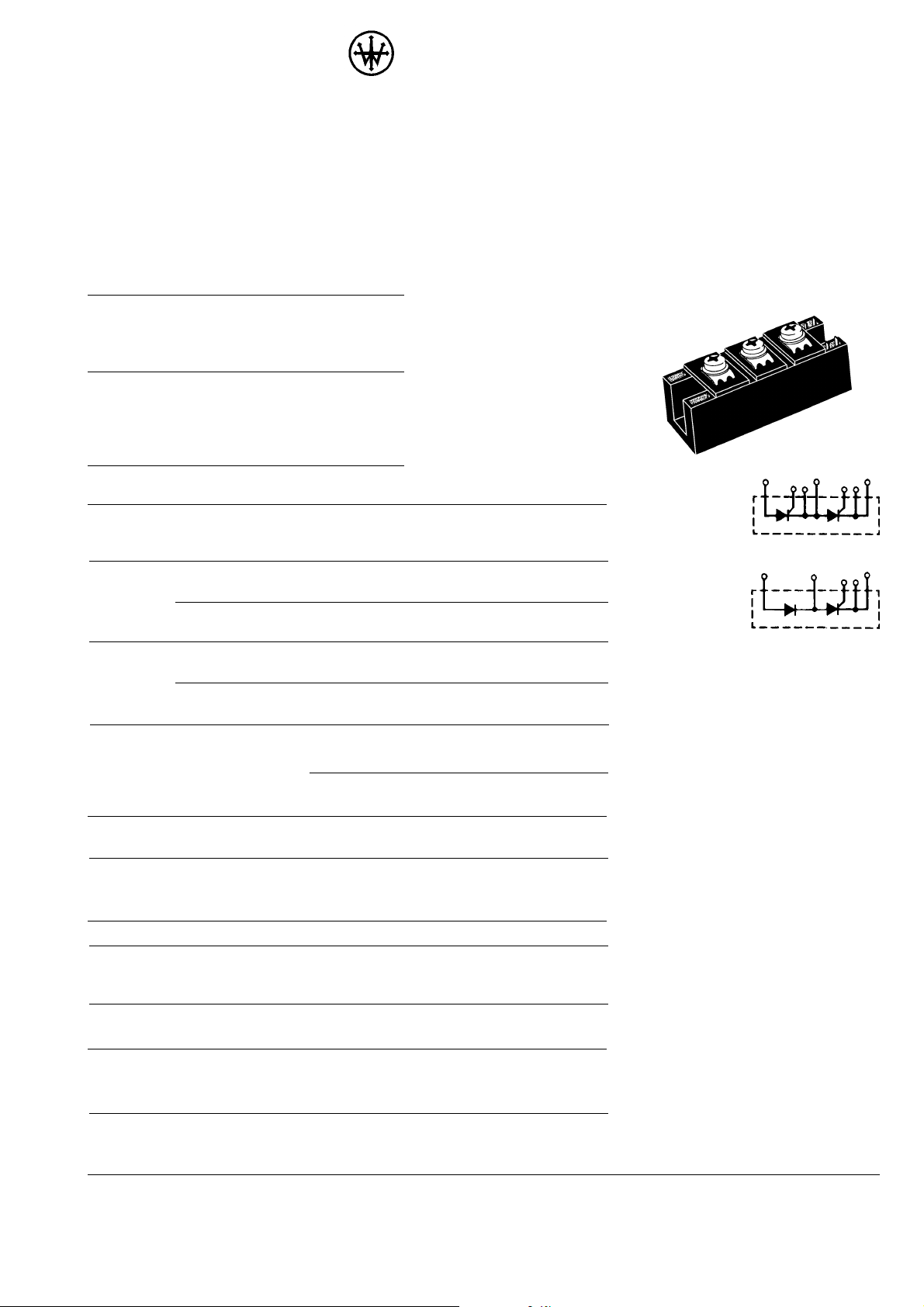
WPT 162
1 5 4 2
3
WPH 162
Features
●
International standard package
●
Direct copper bonded Al2O3 -ceramic
base plate
●
Planar passivated chips
●
Isolation voltage 3600 V~
●
Keyed gate/cathode twin pins
Applications
●
Motor control
●
Power converter
●
Heat and temperature control for
industrial furnaces and chemical
processes
●
Lighting control
●
Contactless switches
Advantages
●
Space and weight savings
●
Simple mounting
●
Improved temperature and power
cycling
●
Reduced protection circuits
7
4
5
5 4 236 7 1
Symbol Test Conditions Characteristic Values
, I
I
RRM
DRM
, V
V
T
F
V
T0
r
T
V
GT
I
GT
V
GD
I
GD
I
L
I
H
t
gd
t
q
Q
S
I
RM
R
thJC
R
thJK
d
S
d
A
a Maximum allowable acceleration 50 m/s
TVJ= T
; VR = V
VJM
RRM
; VD = V
DRM
10 mA
IT, IF = 300 A; TVJ = 25°C 1.25 V
For power-loss calculations only (TVJ = 125°C) 0.88 V
1.15 mΩ
VD = 6 V; TVJ = 25°C 2.5 V
TVJ = -40°C 2.6 V
VD = 6 V; TVJ = 25°C 150 mA
TVJ = -40°C 200 mA
TVJ = T
;V
VJM
D
= 2/3 V
DRM
0.2 V
10 mA
TVJ = 25°C; tP = 30 µs; VD = 6 V 300 mA
IG = 0.5 A; diG/dt = 0.5 A/µs
TVJ = 25°C; VD = 6 V; RGK = ∞ 200 mA
TVJ = 25°C; VD = 1/2 V
IG = 0.5 A; diG/dt = 0.5 A/µs
TVJ = T
VR = 100 V; dv/dt = 20 V/µs; VD = 2/3 V
TVJ = T
; IT = 300 A, tP = 200 µs; -di/dt = 10 A/µs typ. 150 µs
VJM
; IT, IF = 300 A, -di/dt = 50 A/µs 550 µC
VJM
DRM
DRM
2 µs
235 A
per thyristor/diode; DC current 0.155 K/W
per module other values 0.0775 K/W
per thyristor/diode; DC current see Fig. 8/9 0.225 K/W
per module 0.1125 K/W
Creepage distance on surface 12.7 m m
Strike distance through air 9.6 mm
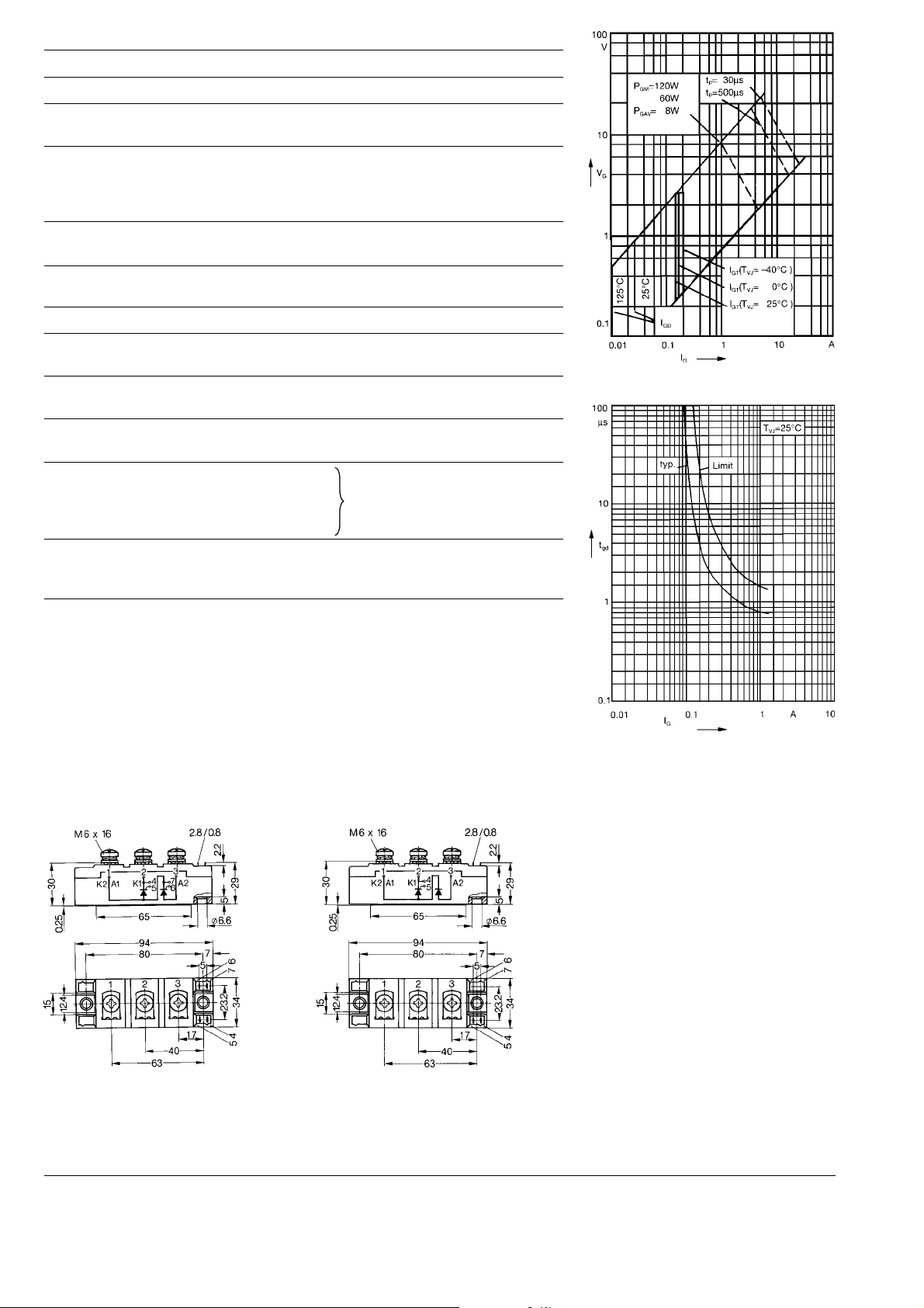
Fig. 1 Gate trigger characteristics
2
Optional accessories for modules
Keyed gate/cathode twin plugs with wire length = 350 mm, gate = yellow, cathode = red
Type U9911 UL 758, style 1385,
CSA class 5851, guide 460-1-1
Dimensions in mm (1 mm = 0.0394")
WPT 162 WPH 162
Fig. 2 Gate trigger delay time
 Loading...