

Westcode Semiconductors W3128V#300, W3128V#400 Data Sheet
Date:- 11, July 2005
WESTCODE
An IXYS Company
Rectifier Diode
Types W3128V#300-W3128V#400
Old Type No.: SW26-40DXC13C
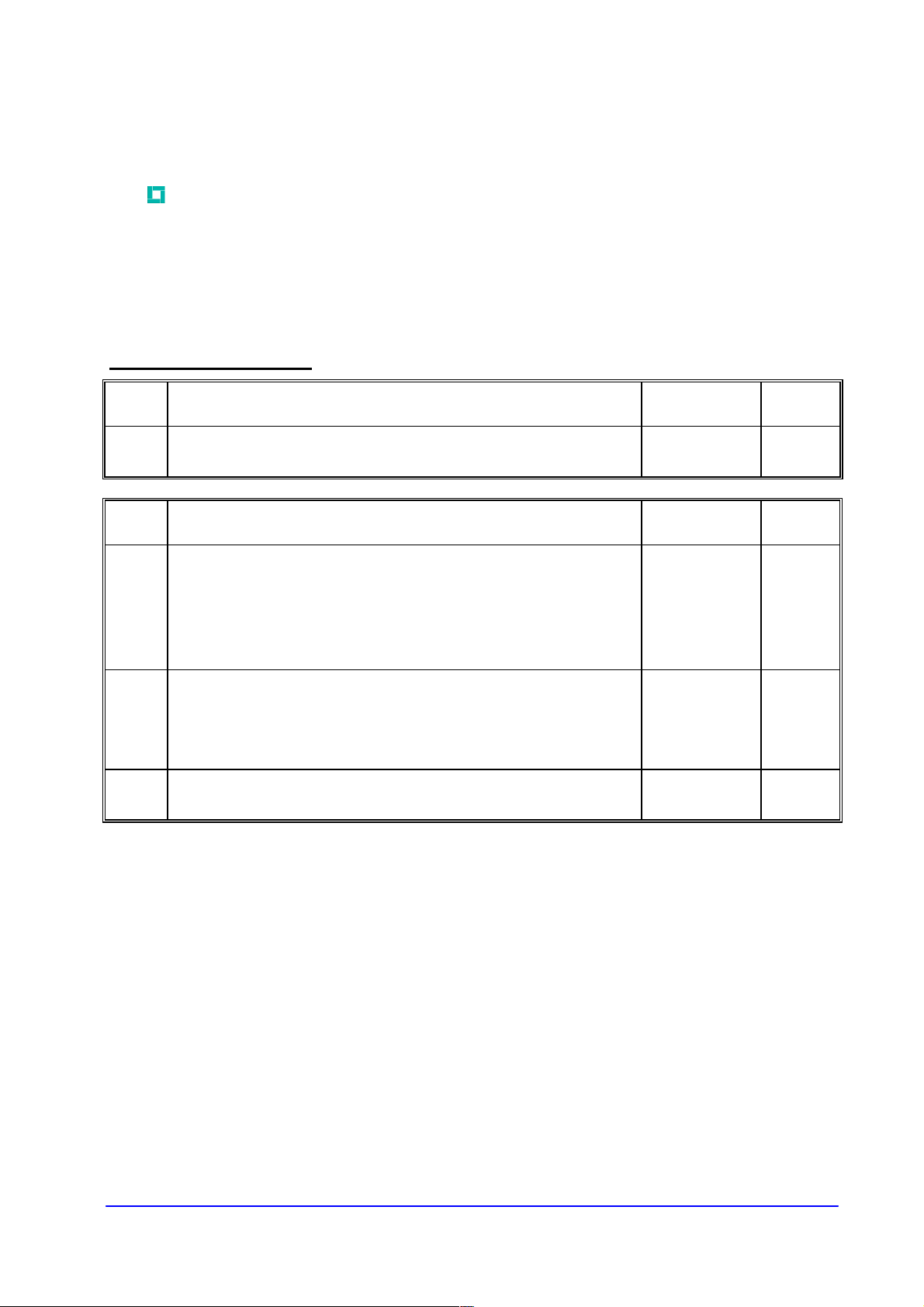
Absolute Maximum Ratings
VOLTAGE RATINGS
V
RRM
V
RSM
I
F(AV)M
I
F(AV)M
I
F(AV)M
I
F(RMS)M
I
F(d.c.)
I
FSM
I
FSM2
I2tI
I2t
T
j op
T
stg
Repetitive peak reverse voltage, (note 1) 3000-4000 V
Non-repetitive peak reverse voltage, (note 1) 3100-4100 V
OTHER RATINGS
Maximum average forward current, T
Maximum average forward current. T
Maximum average forward current. T
Nominal RMS forward current, T
D.C. forward current, T
Peak non-repetitive surge tp=10ms, Vrm=60%V
Peak non-repetitive surge tp=10ms, Vrm≤10V, (note 5)
2
t capacity for fusing tp=10ms, Vrm=60%V
I2t capacity for fusing tp=10ms, Vrm≤10V, (note 5)
Operating temperature range -55 to +160 °C
Storage temperature range -55 to +200 °C
=25°C, (note 4) 5046 A
sink
=55°C, (note 2) 3128 A
sink
=100°C, (note 2) 2174 A
sink
=100°C, (note 3) 1340 A
sink
=25°C, (note 2) 5750 A
sink
, (note 5) 30 kA
RRM
, (note 5) 4.50×10
RRM
Data Sheet Issue:- 1
MAXIMUM
LIMITS
MAXIMUM
LIMITS
33 kA
6
5.45×10
6
UNITS
UNITS
A2s
A2s
Notes:-
1) De-rating factor of 0.13% per °C is applicable for T
2) Double side cooled, single phase; 50Hz, 180° half-sinewave.
3) Single side cooled, single phase; 50Hz, 180° half-sinewave.
4) Double side cooled.
5) Half-sinewave, 160°C T
Data Sheet. Types W3128V#300 to W3128V#400 Issue 1 Page 1 of 9 July, 2005
initial.
j
below 25°C.
j
WESTCODE
WESTCODE An IXYS Company Rectifier Diode Types W3128V#300 to W3128V#400
WESTCODEWESTCODE
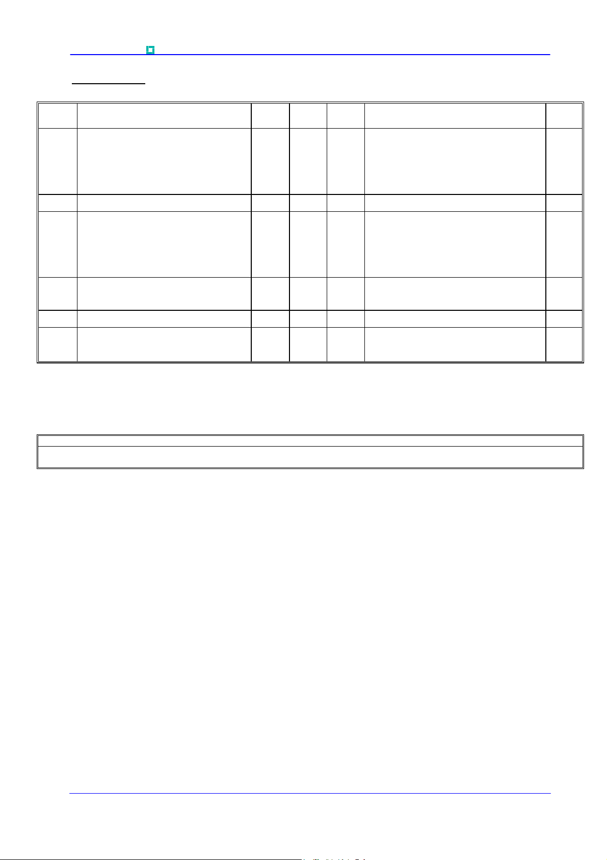
Characteristics
PARAMETER MIN. TYP. MAX. TEST CONDITIONS (Note 1) UNITS
V
V
V
r
I
Q
Q
I
t
R
FM
FM
T0
T
RRM
rr
ra
rr
rr
thJK
Maximum peak forward voltage - - 1.95 IFM=6800A V
Maximum peak forward voltage - - 2.35 IFM=9450A V
Threshold voltage - - 0.875 V
Slope resistance - - 0.158
Peak reverse current - - 60 Rated V
RRM
mΩ
mA
Recovered charge - 7000 - µC
Recovered charge, 50% Chord - 4200 5000 µC
Reverse recovery current - 210 - A
Reverse recovery time - 40 -
Thermal resistance, junction to heatsink
- - 0.016 Double side cooled K/W
I
=1000A, tp=1000µs, di/dt=10A/µs,
FM
V
=50V
r
µs
- - 0.032 Single side cooled K/W
F Mounting force 27 - 34 kN
- 1000 - Outline Options VC & VT
W
Weight
t
Notes:-
1) Unless otherwise indicated T
=160°C.
j
800 Outline Option VF & VV
g
2) For other clamp forces, please consult factory.
Notes on rupture rated packages.
This product is available with a non-rupture rated package.
For additional details on these products, please consult factory.
Data Sheet. Types W3128V#300 to W3128V#400 Issue 1 Page 2 of 9 July, 2005
WESTCODE
WESTCODE An IXYS Company Rectifier Diode Types W3128V#300 to W3128V#400
WESTCODEWESTCODE
Notes on Ratings and Characteristics
1.0 Voltage Grade Table
V
Voltage Grade
30 3000 3100 1800
32 3200 3300 1920
34 3400 3500 2040
36 3600 3700 2160
38 3800 3900 2280
40 4000 4100 2400
2.0 Extension of Voltage Grades
This report is applicable to other voltage grades when supply has been agreed by Sales/Production.
3.0 De-rating Factor
A blocking voltage de-rating factor of 0.13%/°C is applicable to this device for Tj below 25°C.
4.0 Snubber Components
When selecting snubber components, care must be taken not to use excessively large values of snubber
capacitor or excessively small values of snubber resistor. Such excessive component values may lead to
device damage due to the large resultant values of snubber discharge current. If required, please consult
the factory for assistance.
5.0 Computer Modelling Parameters
RRM
V
V
RSM
V
V
R
DC V
5.1 Device Dissipation Calculations
2
I
=
AV
Where VT0=0.875V, rT=0.158mΩ,
R
= Supplementary thermal impedance, see table below and
th
00
2
2
4
2
rff
⋅⋅
T
WrffVV
⋅⋅⋅++−
AVTTT
ff = Form factor, see table below.
Supplementary Thermal Impedance
Conduction Angle 6 phase (60°) 3 phase (120°) ½ wave (180°) d.c.
Square wave Double Side Cooled
Square wave Single Side Cooled
Sine wave Double Side Cooled
Sine wave Single Side Cooled
Conduction Angle 6 phase (60°) 3 phase (120°) ½ wave (180°) d.c.
Square wave 2.449 1.732 1.414 1
Sine wave 2.778 1.879 1.57
0.0205 0.0190 0.0170 0.0160
0.0400 0.0376 0.0340 0.0320
0.0198 0.0177 0.0162
0.0388 0.0355 0.0324
Form Factors
and:
W
AV
=
∆
R
T
th
max
TTT
−=∆
Kj
5.2 Calculating VF using ABCD Coefficients
Data Sheet. Types W3128V#300 to W3128V#400 Issue 1 Page 3 of 9 July, 2005
 Loading...