

Westcode Semiconductors W1074Y#200, W1074Y#320 Data Sheet
Date:- 13 Oct 2004
WESTCODE
An IXYS Company
Rectifier Diode
Types W1074Y#200 to W1074Y#320
Old Type No.: SW20-32CXC445
Absolute Maximum Ratings
VOLTAGE RATINGS
V
RRM
V
RSM
I
F(AV)M
I
F(AV)M
I
F(AV)M
I
F(RMS)M
I
F(d.c.)
I
FSM
I
FSM2
I2tI
I2t
T
j op
T
stg
Repetitive peak reverse voltage, (note 1) 2000-3200 V
Non-repetitive peak reverse voltage, (note 1) 2100-3300 V
OTHER RATINGS
Maximum average forward current, T
Maximum average forward current. T
Maximum average forward current. T
Nominal RMS forward current, T
D.C. forward current, T
Peak non-repetitive surge tp=10ms, Vrm=60%V
Peak non-repetitive surge tp=10ms, Vrm≤10V, (note 5)
2
t capacity for fusing tp=10ms, Vrm=60%V
2
t capacity for fusing tp=10ms, Vrm≤10V, (note 5)
I
Operating temperature range -40 to +160 °C
Storage temperature range -40 to +200 °C
=25°C, (note 4) 1704 A
sink
=55°C, (note 2) 1074 A
sink
=100°C, (note 2) 736 A
sink
=100°C, (note 3) 444 A
sink
=25°C, (note 2) 1984 A
sink
, (note 5) 10.8 kA
RRM
, (note 5) 583×10
RRM
Data Sheet Issue:- 1
MAXIMUM
LIMITS
MAXIMUM
LIMITS
11.8 kA
3
3
706×10
UNITS
UNITS
A2s
A2s
Notes:-
1) De-rating factor of 0.13% per °C is applicable for T
2) Double side cooled, single phase; 50Hz, 180° half-sinewave.
3) Single side cooled, single phase; 50Hz, 180° half-sinewave.
4) Double side cooled.
5) Half-sinewave, 160°C T
Data Sheet. Types W1074Y#200 to W1074Y#320 Issue 1 Page 1 of 9 October, 2004
initial.
j
below 25°C.
j
WESTCODE
WESTCODE An IXYS Company Rectifier Diode Types W1074Y#200 to W1074Y#320
WESTCODEWESTCODE
Characteristics
PARAMETER MIN. TYP. MAX. TEST CONDITIONS (Note 1) UNITS
V
V
r
I
I
Q
Q
I
t
R
FM
T0
T
RRM
RRM
rr
ra
rr
rr
thJK
Maximum peak forward voltage - - 2.13 IFM=3090A V
Threshold voltage - - 0.92 V
Slope resistance - - 0.39
Peak reverse current - - 30 Rated V
Peak reverse current - - 30 Rated V
RRM
, Tj=25°C mA
RRM
mΩ
mA
Recovered charge - 1800 - µC
Recovered charge, 50% Chord - 900 1450 µC
Reverse recovery current - 100 - A
Reverse recovery time - 18 -
Thermal resistance, junction to heatsink
- - 0.05 Double side cooled K/W
I
=500A, tp=500µs, di/dt=10A/µs, Vr=50V
TM
µs
- - 0.10 Single side cooled K/W
F Mounting force 5.5 - 8.3 kN
W
Weight
t
Notes:-
1) Unless otherwise indicated T
=160°C.
j
- 90 - Housing option YC
- 140 - Housing option YH
g
Data Sheet. Types W1074Y#200 to W1074Y#320 Issue 1 Page 2 of 9 October, 2004
WESTCODE
WESTCODE An IXYS Company Rectifier Diode Types W1074Y#200 to W1074Y#320
WESTCODEWESTCODE
Notes on Ratings and Characteristics
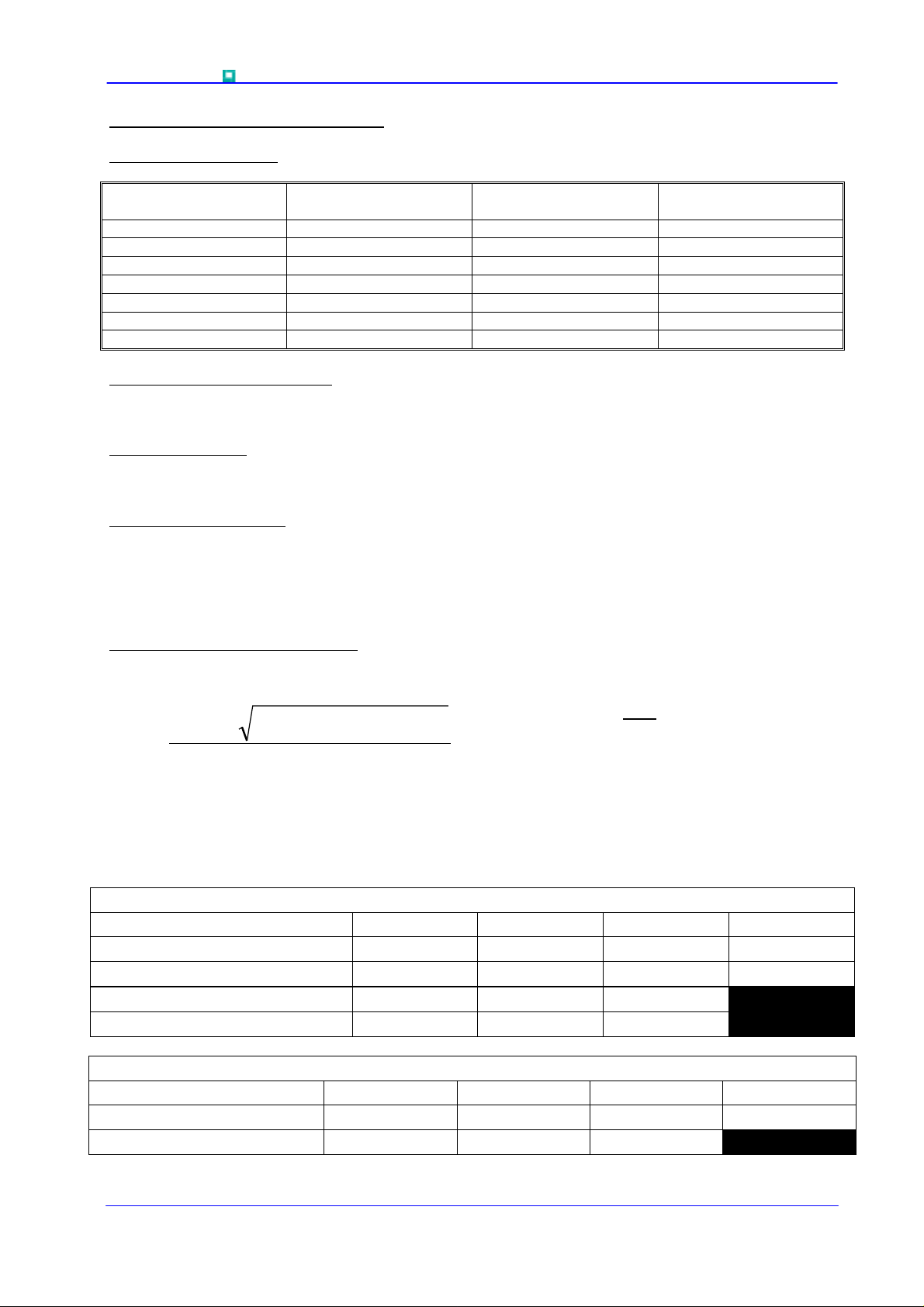
1.0 Voltage Grade Table V
Voltage Grade
20 2000 2100 1250
22 2200 2300 1350
24 2400 2500 1450
26 2600 2700 1550
28 2800 2900 1650
30 3000 3100 1750
32 3200 3300 1850
2.0 Extension of Voltage Grades
This report is applicable to other voltage grades when supply has been agreed by Sales/Production.
3.0 De-rating Factor
A blocking voltage de-rating factor of 0.13%/°C is applicable to this device for Tj below 25°C.
4.0 Snubber Components
When selecting snubber components, care m ust be taken not to use ex cessively large values of snubber
capacitor or excessively sm all values of snubber re sistor. Such exc essive com ponent values may lead to
device damage due to the large resultant values of snubber disc harge current. If r equired, please consult
the factory for assistance.
5.0 Computer Modelling Parameters
DRM VDSM VRRM
V
V
RSM
V
V
V
D
DC V
R
5.1 Device Dissipation Calculations
T
2
I
=
AV
Where VT0=0.92V, rT=0.39mΩ,
R
= Supplementary thermal impedance, see table below and
th
00
2
2
4
2
rff
⋅⋅
T
WrffVV
⋅⋅⋅++−
AVTTT
and:
W
AV
=
∆
R
max
th
TTT
−=∆
Kj
ff = Form factor, see table below.
Supplementary Thermal Impedance
Conduction Angle 6 Phase (60°) 3 Phase (120°) ½ Wave (180°) d.c.
Square wave Double Side Cooled
Square wave Single Side Cooled
Sine wave Double Side Cooled
Sine wave Single Side Cooled
Conduction Angle 6 Phase (60°) 3 Phase (120°) ½ Wave (180°) d.c.
Square wave 2.449 1.732 1.414 1
Sine wave 2.778 1.879 1.57
0.069 0.061 0.057 0.05
0.119 0.111 0.107 0.1
0.052 0.0513 0.0505
0.102 0.1013 0.1005
Form Factors
Data Sheet. Types W1074Y#200 to W1074Y#320 Issue 1 Page 3 of 9 October, 2004
 Loading...