Date:- 30 Jun, 2004
WESTCODE
An
Absolute Maximum Ratings
V
DRM
V
DSM
V
RRM
V
RSM
I
TGQ
L
s
I
T(AVM)
I
T(RMS)
I
TSM
I
TSM2
I2tI
di/dt
P
FGM
P
RGM
I
FGM
V
RGM
t
off
t
on
T
j op
T
stg
IXYS
Company
Symmetrical Gate Turn-Off Thyristor
Type S0700KC17#
VOLTAGE RATINGS
Repetitive peak off-state voltage, (note 1) 1700 V
Non-repetitive peak off-state voltage, (note 1) 1800 V
Repetitive peak reverse voltage 100-1360 V
Non-repetitive peak reverse voltage 100-1360 V
RATINGS
Peak turn-off current, (note 2) 700 A
Snubber loop inductance, ITM=I
Mean on-state current, T
Nominal RMS on-state current, 25°C (note 3) 870 A
Peak non-repetitive surge current tp=10ms 5 kA
Peak non-repetitive surge current, (Note 4) 9 kA
2
t capacity for fusing tp=10ms 125×10
Critical rate of rise of on-state current, (note 5) 1000 A/µs
cr
Peak forward gate power 160 W
Peak reverse gate power 5 kW
Peak forward gate current 100 A
Peak reverse gate voltage (note 6). 18 V
Minimum permissible off-time, ITM=I
Minimum permissible on-time 20 µs
Operating temperature range -40 to +125 °C
Storage temperature range -40 to +150 °C
sink
, (note 2) 0.3 µH
TGQ
=55°C (note 3) 430 A
, (note 2) 70 µs
TGQ
Data Sheet Issue:- 1
MAXIMUM
LIMITS
MAXIMUM
LIMITS
3
UNITS
UNITS
A2s
Notes:-
=-2Volts.
1) V
GK
=125°C, VD=80%VDM, VDM<V
2) T
j
3) Double-side cooled, single phas e; 50Hz, 180° half-sinewave.
4) Half-sinewave, t
5) For di/dt>1000A/µs, consult factory.
6) May exceed this value during turn-off avalanche period.
Data Sheet. Type S0700KC17# Issue 1 Page 1 of 15 July, 2004
=2ms
p
, diGQ/dt=20A/µs, ITM=I
DRM
& CS=1.5µF.
TGQ

WESTCODE
WESTCODE
WESTCODE WESTCODE
An IXYS Company
Characteristics
Symmetrical Gat e Turn-Off Thyristor type S0700KC17#
Parameter MIN TYP MAX TEST CONDITIONS
V
TM
I
L
I
H
dv/dtcrCritical rate of rise of off-state voltage 800 - - VD=80%V
I
DM
I
RM
I
GKM
V
GT
GT
t
d
t
gt
Maximum peak on-state voltage - 1.9 2.2 IG=1.5A, IT=700A V
Latching current - 5 - Tj=25°C A
Holding current. - 5 - Tj=25°C A
Peak off state current - - 30 Rated V
Peak reverse current - - 40 Rated V
Peak negative gate leakage current - - 200 VGR=-16V mA
Gate trigger voltage
Gate trigger current
-0.9-T
-0.8-T
-0.7-T
-1.56T
-0.51T
=-40°C V
j
=25°C
j
=125°C V
j
=-40°C A
j
=25°C
j
- 125 400 Tj=125°C mA
VD=50%V
Delay time - 0.8 -
T
=25°C, di/dt=300A/µs, (10%IGM to 90%VD)
j
Turn-on time - 3 5 Conditions as for td, (10%IGM to 10%VD)µs
, VGR=-2V V/µs
DRM
, VGR=-2V mA
DRM
RRM
=25V, RL=25m
V
D
VD=25V, RL=25m
, I
DRM
=700A, IGM=12A, diG/dt=6A/µs µs
TGQ
Ω
Ω
UNITS
mA
V
AI
t
f
t
gq
I
gq
Q
t
tail
t
gw
Fall time - 0.8 -
/dt=20A/µs, VGR=-16V, (90%I
di
GQ
Turn-off time - 10 11 Conditions as for tf, (10%IGQ to 10%I
Turn-off gate current - 190 - Conditions as for t
Turn-off gate charge - 1.3 1.45 Conditions as for t
gq
Tail time - 30 50 Conditions as for tf, (10%I
Gate off-time (see note 3). 100 - - Conditions as for t
VD=50%V
DRM
, I
=700A, CS=1.5µF,
TGQ
f
f
f
TGQ
to 10%I
TGQ
)µs
TGQ
to I
<1A) µs
TGQ
TGQ
)
µs
A
mC
µs
- - 0.063 Double side cooled K/W
R
thJK
Thermal resistance junction to sink
- - 0.21 Cathode side cooled K/W
- - 0.09 Anode side cooled K/W
F Mounting force 4.5 - 9.0 (see note 2) kN
W
Weight - 120 - g
t
Notes:-
1) Unless otherwise indic at ed T
2) For other clamping f orces, consult factory.
3) The gate off-tim e i s the period during which the gate circuit i s
required to remain low impedance to al l ow for t he passage
of tail current.
=125oC.
j
Data Sheet. Type S0700KC17# Issue 1 Page 2 of 15 July, 2004

WESTCODE
WESTCODE
WESTCODE WESTCODE
An IXYS Company
Symmetrical Gat e Turn-Off Thyristor type S0700KC17#
Notes on ratings and characteristics.
1. Maximum Ratings.
1.1 Off-state voltage ratings. Unless otherwise indicated, all off-state voltage ratings are given for gate conditions as diagram 1. For other gate conditions see the curves of figure 5. It should be noted that V
is the repeatable peak
DRM
voltage which may be applied to the device and does not relate to a DC operating condition. W hile not
given in the ratings, V
should ideally be limited to 60% V
DC
in this product.
DRM
Diagram 1.
1.2 Reverse voltage rating. All devices in this series have a m inim um V 80%V
is available.
DRM
of 100 Volts. If specified at the tim e of order , a V
RRM
RRM
up to
1.3 Peak turn-off current. The figure given in maximum ratings is the highest value for normal operation of the device under conditions given in note 2 of ratings. For other com binations of I
, VD and Cs see the curves of figures
TGQ
15 & 16. The curves are eff ective over the normal operating range of the device and as sume a snubber
circuit equivalent to that given in diagram 2. If a m ore com plex snubber, s uch as an Under land circuit, is
employed then the equivalent C
should be used and Ls<0.3µH must be ensured for the curves to be
S
applied.
L
s
D
s
C
s
Diagram 2.
R
1.4 R.M.S and average current. Measured as for standard thyristor conditions, double side cooled, single phase, 50Hz, 180° halfsinewave. These are included as a guide to com pare the alternative types of G TO thyristors available, values can not be applied to practical applications, as they do not include switching losses.
2
1.5 Surge rating and I
t.
Ratings are for half-sinewave, peak value against duration is given in the curve of figure 4.
1.6 Snubber loop inductance. Use of GTO thyristors with snubber loop inductance, L
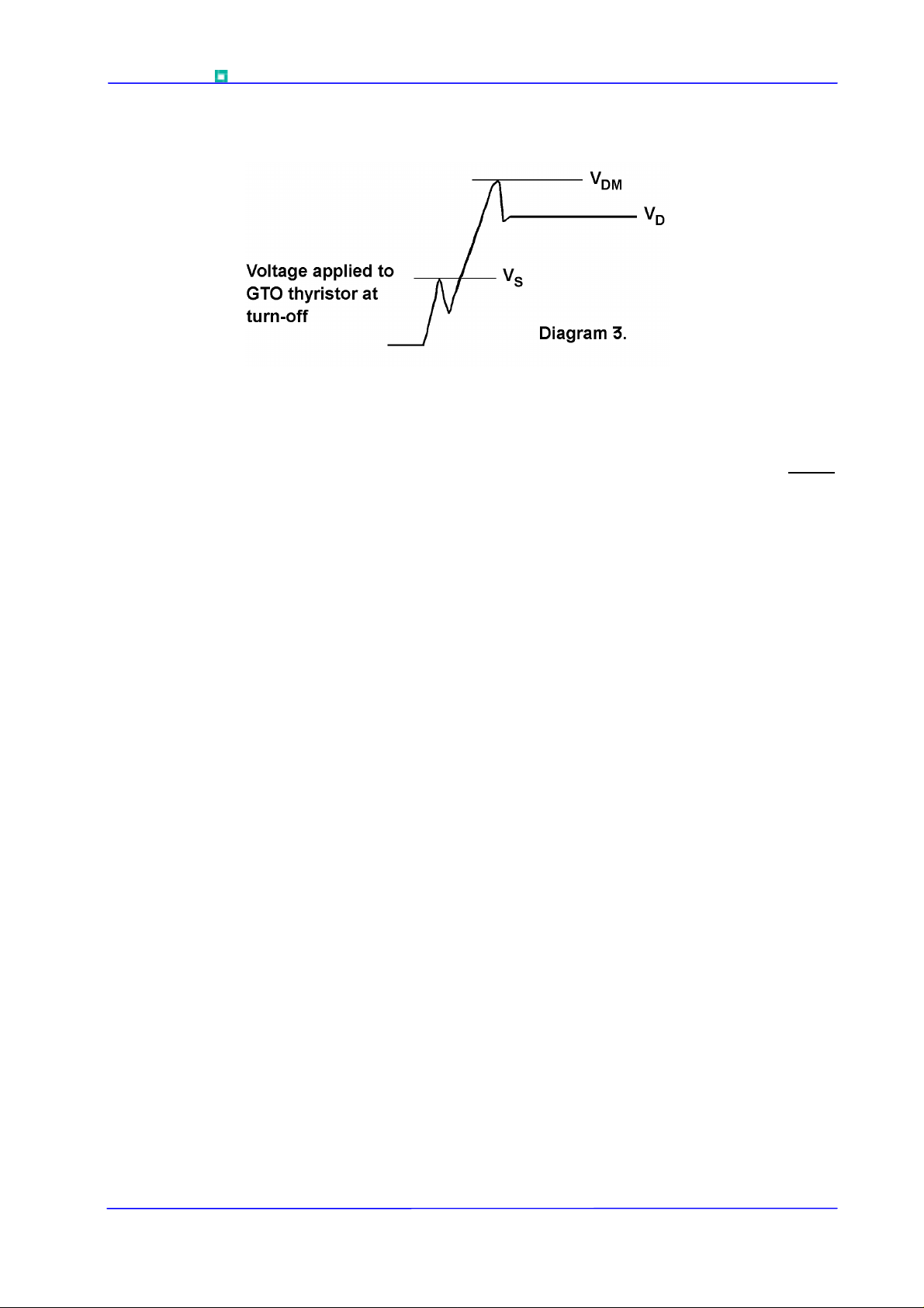
<0.3µH implies no dangerous Vs voltages (see
s
diagrams 2 & 3) can be applied, provided the other conditions given in note 1.3 are enforced. Alternatively
should be limited to 600 Volts to avoid possible device failure.
V
s
Data Sheet. Type S0700KC17# Issue 1 Page 3 of 15 July, 2004

WESTCODE
WESTCODE
WESTCODE WESTCODE
An IXYS Company
Symmetrical Gat e Turn-Off Thyristor type S0700KC17#
1.7 Critical rate of rise of on-state current The value given is the maxim um r epetitive rating, but does not im ply any specific operating condition. T he high turn-on losses associated with limit di/dt would not allow for practical duty cycle at this maxim um condition. For special pulse applications, s uch as crowbars and puls e power supplies , a m uch higher di/dt is possible. Where the device is required to operate with infrequent high current pulses, with natural commutation (i.e. not gate turn-off), then di/dt>3kA/µs is possible. For this type of operation individual specific evaluation is required.
1.8 Gate ratings The absolute conditions above which the gate may be damaged. It is permitted to allow V off (see diagram 10) to exceed V
which is the implied DC condition.
RGM
GK(AV)
during turn-
1.9 Minimum permissible off time. This time relates specif ically to re-firing of device (see also note on gate-off time 2.7). T he value given in the ratings applies only to operating conditions of ratings note 2. For other operating conditions see the curves of figure 18.
1.10 Minimum permissible on-time. Figure is given for minim um tim e to allow complete conduction of all the GT O thyristor islands. W here a simple snubber, of the form given in diagram 1. (or any other non-energy recovery type which discharges through the GTO at turn-on) the ac tual minimum on-time will usually be fixed by the snubber circuit time constant, which must be allowed to fully discharge before the GTO thyristor is turned off. If the anode circuit has di/dt<10A/µs then the minimum on-tim e s hould be incr eas ed, the actual value will depend upon the di/dt and operating conditions (each case needs to be assessed on an individual basis).
Data Sheet. Type S0700KC17# Issue 1 Page 4 of 15 July, 2004

WESTCODE
WESTCODE
WESTCODE WESTCODE
An IXYS Company
Symmetrical Gat e Turn-Off Thyristor type S0700KC17#
2 Characteristics
2.1 Instantaneous on-state voltage Measured using a 500µs square pulse, see also the curves of figure 2 for other values of I
TM
.
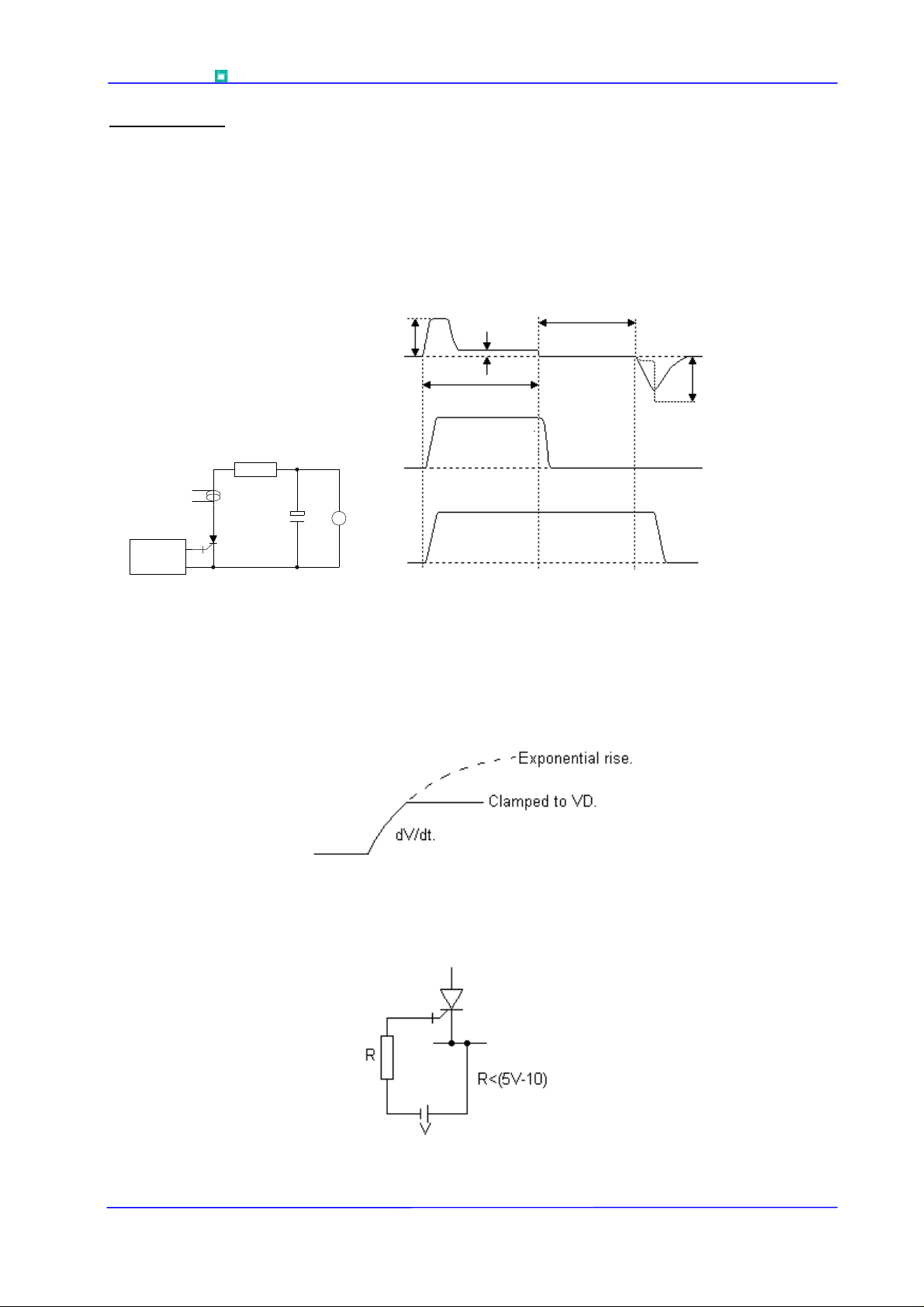
2.2 Latching and holding current These are considered to be approximately equal and only the latching current is measured, type test only as outlined below. The test circuit and wave diagrams are given in diagram 4. The anode current is monitored on an oscilloscope while V period between the end of I
and the application of reverse gate voltage. Test fr equency is 100Hz with I
G
is increased, until the current is s een to flow during the un-gated
D
GM
& IG as for td of characteristic data.
I
Gate-drive
I
GM
R1
CT
C1
Vs
DUT
G
200µs
200µs
Unlatched
Latched
Gate current
15V
Anode current
unlatched condition
Anode current
Latched condition
Diagram 4, Latching test circuit and waveforms.
2.3 Critical dv/dt The gate conditions are the sam e as for 1.1, this c haracteristic is for off -state only and does not relate to dv/dt at turn-off. The measurem ent, type test only, is conducted using the exponential ramp method as shown in diagram 5. It should be noted that GTO thyristors have a poor static dv/dt c apability if the gate is open circuit or R
is high impedance. Typical values: - dv/dt<30V/µs for RGK>10Ω.
GK
Diagram 5, Definition of dV/dt.
2.4 Off-state leakage. For I
DRM
& I
see notes 1.1 & 1.2 for gate leakage IGK, the off-state gate circuit is required to sink this
RRM
leakage and still maintain minimum of –2 Volts. See diagram 6.
Diagram 6.
Data Sheet. Type S0700KC17# Issue 1 Page 5 of 15 July, 2004
 Loading...