

Westcode Semiconductors R325CH02, R325CH14 Data Sheet

Date:- 21 Dec, 2000
WESTCODE
Distributed Gate Thyristor
Types R325CH02 to R325CH14
Absolute Maximum Ratings
VOLTAGE RATINGS
V
DRM
V
DSM
V
RRM
V
RSM
I
T(AV)
I
T(AV)
I
T(AV)
I
T(RMS)
I
T(d.c.)
I
TSM
I
TSM2
I2tI
I2t
diT/dt
V
RGM
P
G(AV)
P
GM
V
GD
T
HS
T
stg
Repetitive peak off-state voltage, (note 1) 200-1400 V
Non-repetitive peak off-state voltage, (note 1) 200-1400 V
Repetitive peak reverse voltage, (note 1) 200-1400 V
Non-repetitive peak reverse voltage, (note 1) 300-1500 V
OTHER RATINGS
Mean on-state current, T
Mean on-state current. T
Mean on-state current. T
Nominal RMS on-state current, T
D.C. on-state current, T
Peak non-repetitive surge tp=10ms, VRM=0.6V
Peak non-repetitive surge tp=10ms, V
2
t capacity for fusing tp=10ms, VRM=0.6V
2
t capacity for fusing tp=10ms, V
I
Maximum rate of rise of on-state current (repetitive), (Note 6) 1000 A/µs
Maximum rate of rise of on-state current (non-repetitive), (Note 6) 1500 A/µs
Peak reverse gate voltage 5 V
Mean forward gate power 2 W
Peak forward gate power 30 W
Non-trigger gate voltage, (Note 7) 0.25 V
Operating temperature range -40 to +125 °C
Storage temperature range -40 to +150 °C
=55°C, (note 2) 1178 A
sink
=85°C, (note 2) 767 A
sink
=85°C, (note 3) 433 A
sink
=25°C, (note 2) 2395 A
sink
=25°C, (note 4) 892 A
sink
, (note 5) 17 kA
RRM
≤
10V, (note 5)
RM
, (note 5) 1.45×10
RRM
≤
10V, (note 5)
RM
Data Sheet Issue:- 1
MAXIMUM
LIMITS
MAXIMUM
LIMITS
18.7 kA
6
1.75×10
6
UNITS
UNITS
A2s
A2s
Notes:-
1)
De-rating factor of 0.13% per °C is applicable for Tj below 25°C.
2)
Double side cooled, single phase; 50Hz, 180° half-sinewave.
3)
Single side cooled, single phase; 50Hz, 180° half-sinewave.
4)
Double side cooled.
5)
Half-sinewave, 125°C Tj initial.
6)
VD=67% V
7)
Rated V
Data Sheet. Types R325CH02 to R325CH14 Issue 1 Page 1 of 12 December, 2000
DRM
, IFG=2A, t
DRM
.
≤
0.5µs, T
r
case
=125°C.

WESTCODE
Positive development in power electronics
Characteristics
R325CH02 to R325CH14
PARAMETER MIN. TYP. MAX. TEST CONDITIONS
V
V
r
dv/dt Critical rate of rise of off-state voltage - - 200 VD=80% V
I
I
V
I
I
Q
t
R
Maximum peak on-state voltage - - 2.2 ITM=2000A V
TM
Threshold voltage - - 1.6 V
0
Slope resistance - - 0.3
S
Peak off-state current - - 150 Rated V
DRM
Peak reverse current - - 150 Rated V
RRM
Gate trigger voltage - - 3.0 Tj=25°C V
GT
Gate trigger current - - 300 Tj=25°C VD=10V, IT=2A mA
GT
Holding current - - 1000 Tj=25°C mA
H
Recovered charge, 50% Chord - 170 190
ra
--35
Turn-off time
q
25 - 40
Thermal resistance, junction to
θ
heatsink
- - 0.024 Double side cooled
- - 0.048 Single side cooled
ITM=1000A, tp=1000µs, di/dt=60A/µs,
V
ITM=1000A, tp=1000µs, di/dt=60A/µs,
V
ITM=1000A, tp=1000µs, di/dt=60A/µs,
V
DRM
RRM
=50V
r
=50V, Vdr=80%V
r
=50V, Vdr=80%V
r
DRM
(Note 1)
, dVdr/dt=20V/µs
DRM
, dVdr/dt=200V/µs
DRM
UNITS
m
V/µs
mA
µC
µs
K/W
F Mounting force 19 - 26 kN
W
Weight - 510 - g
t
Ω
Notes:-
Unless otherwise indicated Tj=125°C.
1)
Data Sheet. Types R325CH02 to R325CH14 Issue 1 Page 2 of 12 December, 2000

WESTCODE
Notes on Ratings and Characteristics
1.0 Voltage Grade Table
Positive development in power electronics
R325CH02 to R325CH14
V
Voltage Grade 'H'
02 200 210 140
04 400 410 260
06 600 610 420
08 800 810 560
10 1000 1100 700
12 1200 1300 810
14 1400 1400 930
2.0 Extension of Voltage Grades This report is applicable to other and higher voltage grades when supply has been agreed by
Sales/Production.
3.0 Extension of Turn-off Time This Report is applicable to other tq/re-applied dv/dt combinations when supply has been agreed by
Sales/Production.
4.0 Repetitive dv/dt Higher dv/dt selections are available up to 1000V/µs on request.
5.0 De-rating Factor
DRM VDSM VRRM
V
V
RSM
V
V
V
D
DC V
R
A blocking voltage de-rating factor of 0.13%/°C is applicable to this device for Tj below 25°C.
6.0 Rate of rise of on-state current The maxim um un-primed rate of rise of on-s tate current must not exceed 1500A/µs at any time dur ing
turn-on on a non-repetitive basis. For repetitive per formanc e, the on-state r ate of r ise of c urrent m ust not
exceed 1000A/µs at any time during turn-on. Note that these values of rate of rise of current apply to the
total device current including that from any local snubber network.
7.0 Square wave ratings These ratings are given for load component rate of rise of forward current of 100 and 500A/µs.
8.0 Duty cycle lines The 100% duty cycle is represented on all the ratings by a straight line. Other duties can be included as
parallel to the first.
9.0 Maximum Operating Frequency The maximum operating frequenc y is set by the on-state duty, the time required for the thyristor to turn off
) and for the off-state voltage to reach full value (tv), i.e.
(t
q
1
=
max
f
++
ttt
vqpulse
Data Sheet. Types R325CH02 to R325CH14 Issue 1 Page 3 of 12 December, 2000
WESTCODE
(
)
(
)
)
10.0 On-State Energy per Pulse Characteristics These curves enable rapid estim ation of device dissipation to be obtained for conditions not covered by
the frequency ratings.
Then the average dissipation will be:
Positive development in power electronics
be the Energy per pulse for a given current and pulse width, in joules
Let E
p
Let R
and T
be the steady-state d.c. thermal resistance (junction to sink)
th(J-Hs)
be the heat sink temperature.
SINK
R325CH02 to R325CH14
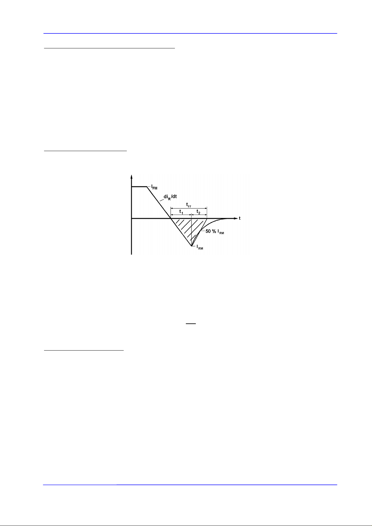
11.0 Reverse recovery ratings (i) Qra is based on 50% Irm chord as shown in Fig. 1 below.
is based on a 150µs integration time.
(ii) Q
rr
i.e.
=
.)(max
150
∫
0
µ
s
rrrr
125
Fig. 1
.
dtiQ
⋅−=⋅=
RWT and fEW
()
−
HsJthAVSINKPAV
1
t
(iii)
12.0 Reverse Recovery Loss
12.1 Determination by Measurement
From waveforms of recovery current obtained from a high frequency shunt (see Note 1, Page 5) and
reverse voltage present during recovery, an instantaneous reverse recovery loss waveform must be
constructed. Let the area under this waveform be E joules per pulse. A new heat sink temperature c an
then be evaluated from the following:
where k = 0.227 (°C/W)/s
E = Area under reverse loss waveform per pulse in joules (W.s)
f = Rated frequency (in Hz) at the original heat sink temperature
R
Data Sheet. Types R325CH02 to R325CH14 Issue 1 Page 4 of 12 December, 2000
= D.C. thermal resistance (°C/W)
th(J-Hs
FactorK
)()(
=
2
t
⋅+⋅−=
RfkETT
()
−
HsJthoriginalSINKnewSINK
 Loading...