

Westcode Semiconductors R1700MC18x, R1700MC21x Data Sheet
Distributed Gate Thyristor
Types R1700MC18x & R1700MC21x
Absolute Maximum Ratings
V
DRM
V
DSM
V
RRM
V
RSM
OTHER RATINGS
I
T(AVM)
I
T(AVM)
I
T(AVM)
I
T(RMS)
I
T(d.c.)
I
TSM
I
TSM2
I2t I2t capacity for fusing tp=10ms, Vrm=0.6V
I2t
(di/dt)
VOLTAGE RATINGS
Repetitive peak off-state voltage, (note 1) 1800-2100 V
Non-repetitive peak off-state voltage, (note 1) 1800-2100 V
Repetitive peak reverse voltage, (note 1) 1800 V
Non-repetitive peak reverse voltage, (note 1) 1900 V
Maximum average on-state current, T
Maximum average on-state current. T
Maximum average on-state current. T
Nominal RMS on-state current, T
D.C. on-state current, T
=25°C, (note 4) 2875 A
sink
Peak non-repetitive surge tp=10ms, Vrm=0.6V
Peak non-repetitive surge tp=10ms, Vrm≤10V, (note 5)
2
I
t capacity for fusing tp=10ms, Vrm≤10V, (note 5)
Critical rate of rise of on-state current (repetitive), (Note 6) 1000 A/µs
Critical rate of rise of on-state current (non-repetitive), (Note 6) 1500 A/µs
cr
Critical rate of rise of on-state current (continuous), (Note 6) 500 A/µs
sink
sink
sink
=25°C, (note 2) 3500 A
sink
Date:- 8
th
April 2014
Data Sheet Issue:- 2
MAXIMUM
LIMITS
MAXIMUM
LIMITS
=55°C, (note 2) 1700 A
=85°C, (note 2) 1150 A
=85°C, (note 3) 610 A
, (note 5) 20 kA
RRM
22 kA
, (note 5) 2.00×10
RRM
2.42×10
6
6
UNITS
UNITS
A2s
A2s
V
P
P
T
T
RGM
G(AV)
GM
j op
stg
Peak reverse gate voltage 5 V
Mean forward gate power 5 W
Peak forward gate power 30 W
Operating temperature range -40 to +125 °C
Storage temperature range -40 to +150 °C
Notes:-
1) De-rating factor of 0.13% per °C is applicable for T
2) Double side cooled, single phase; 50Hz, 180° half-sinewave.
3) Cathode side cooled, single phase; 50Hz, 180° half-sinewave.
4) Double side cooled.
5) Half-sinewave, 125°C T
6) V
=67% V
D
, IFG=2A, tr≤0.5µs, T
DRM
initial.
j
=125°C.
case
below 25°C.
j
Data Sheet. Types R1700MC18x & R1700MC21x Issue 2 Page 1 of 13 April 2014
Distributed Gate Thyristor types R1700MC18x & R1700MC21x
Characteristics
PARAMETER MIN. TYP. MAX. TEST CONDITIONS (Note 1) UNITS
V
TM
V
TM
V
T0
r
T
(dv/dt)crCritical rate of rise of off-state voltage 200 - - VD=80% V
I
DRM
I
RRM
V
GT
I
GT
V
GD
I
H
t
gd
t
gt
Q
rr
Q
ra
I
rm
t
rr
t
q
Maximum peak on-state voltage - - 2.10 ITM=1700A V
Maximum peak on-state voltage - - 2.83 ITM=5100A V
Threshold voltage - - 1.60 V
Slope resistance - - 0.25
, Linear ramp, Gate o/c
DRM
Peak off-state current - - 100 Rated V
Peak reverse current - - 100 Rated V
Gate trigger voltage - - 3.0 V
Tj=25°C VD=10V, IT=3A
DRM
RRM
Gate trigger current - - 300
Gate non-trigger voltage - - 0.25 Rated V
DRM
mΩ
V/µs
mA
mA
mA
V
Holding current - - 1000 Tj=25°C mA
Gate controlled turn-on delay time - 0.5 1.0
Turn-on time - 1.0 2.0
VD=67% V
I
=2A, tr=0.5µs, Tj=25°C
FG
, ITM=1000A, di/dt=60A/µs,
DRM
µs
Recovered charge - 1100 1300 µC
Recovered charge, 50% Chord - 490 - µC
Reverse recovery current - 180 - A
Reverse recovery time - 5.4 -
- 30 -
Turn-off time (note 2)
- 40 -
ITM=1000A, tp=1000µs, di/dt=60A/µs,
V
=50V
r
=1000A, tp=1000µs, di/dt=60A/µs,
I
TM
V
=50V, Vdr=33%V
r
=1000A, tp=1000µs, di/dt=60A/µs,
I
TM
V
=50V, Vdr=33%V
r
, dVdr/dt=20V/µs
DRM
, dVdr/dt=200V/µs
DRM
µs
µs
- - 0.015 Double side cooled K/W
R
thJK
Thermal resistance, junction to heatsink
- - 0.028 Anode side cooled K/W
- - 0.033 Cathode side cooled K/W
F Mounting force 27 - 34 kN
W
t
Weight - 550 - g
Notes:-
1) Unless otherwise indicated T
2)
The required tq (specified with dVdr/dt=200V/µs) is represented by an ‘x’ in the device part number. See ordering information for
details of t
codes.
q
=125°C.
j
Data Sheet. Types R1700MC18x & R1700MC21x Issue 2 Page 2 of 13 April 2014
Distributed Gate Thyristor types R1700MC18x & R1700MC21x
Notes on Ratings and Characteristics
1.0 Voltage Grade Table
Voltage Grade
V
DRM VDSM VRRM
V
V
RSM
V
V
V
D
DC V
R
18 1800 1900 1200
21 2100 2200 1410
2.0 Extension of Voltage Grades
This report is applicable to other and higher voltage grades when supply has been agreed by
Sales/Production.
3.0 Extension of Turn-off Time
This Report is applicable to other t
/re-applied dv/dt combinations when supply has been agreed by
q
Sales/Production.
4.0 Repetitive dv/dt
Higher dv/dt selections are available up to 1000V/µs on request.
5.0 De-rating Factor
A blocking voltage de-rating factor of 0.13%/°C is applicable to this device for T
below 25°C.
j
6.0 Snubber Components
When selecting snubber components, care must be taken not to use excessively large values of snubber
capacitor or excessively small values of snubber resistor. Such excessive component values may lead to
device damage due to the large resultant values of snubber discharge current. If required, please consult
the factory for assistance.
7.0 Rate of rise of on-state current
The maximum un-primed rate of rise of on-state current must not exceed 1500A/µs at any time during
turn-on on a non-repetitive basis. For repetitive performance, the on-state rate of rise of current must not
exceed 1000A/µs at any time during turn-on. Note that these values of rate of rise of current apply to the
total device current including that from any local snubber network.
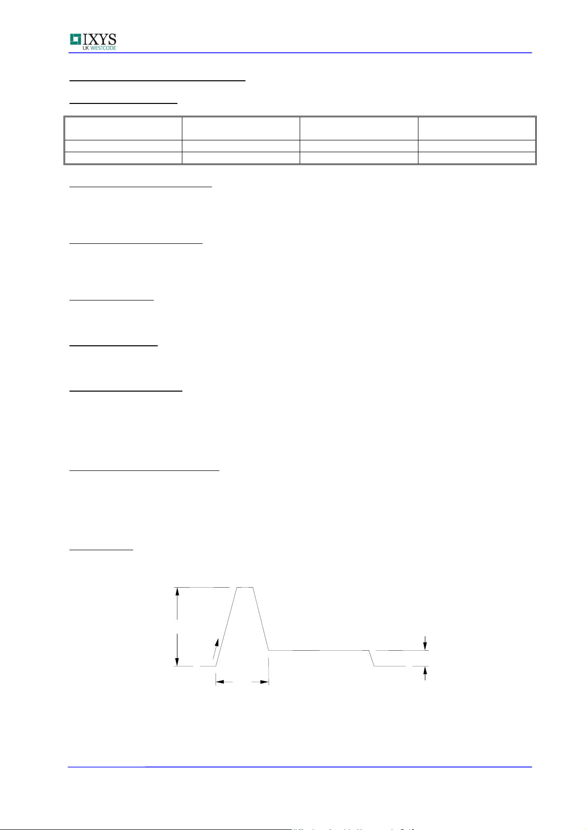
8.0 Gate Drive
The nominal requirement for a typical gate drive is illustrated below. An open circuit voltage of at least
30V is assumed. This gate drive must be applied when using the full di/dt capability of the device.
I
GM
4A/µs
I
G
t
p1
The magnitude of I
(t
) should be 20µs or sufficient to allow the anode current to reach ten times IL, whichever is greater.
p1
should be between five and ten times IGT, which is shown on page 2. Its duration
GM
Otherwise, an increase in pulse current could be needed to supply the necessary charge to trigger. The
‘back-porch’ current I
magnitude in the order of 1.5 times I
should remain flowing for the same duration as the anode current and have a
G
.
GT
Data Sheet. Types R1700MC18x & R1700MC21x Issue 2 Page 3 of 13 April 2014
Distributed Gate Thyristor types R1700MC18x & R1700MC21x
(
)
⋅−=
9.0 Frequency Ratings
The curves illustrated in figures 10 to 18 are for guidance only and are superseded by the maximum
ratings shown on page 1.
10.0 Square wave ratings
These ratings are given for load component rate of rise of forward current of 100 and 500 A/µs.
11.0 Duty cycle lines
The 100% duty cycle is represented on all the ratings by a straight line. Other duties can be included as
parallel to the first.
12.0 Maximum Operating Frequency
The maximum operating frequency is set by the on-state duty, the time required for the thyristor to turn off
) and for the off-state voltage to reach full value (tv), i.e.
(t
q
f
13.0 On-State Energy per Pulse Characteristics
These curves enable rapid estimation of device dissipation to be obtained for conditions not covered by
the frequency ratings.
Let E
Let R
and T
Then the average dissipation will be:
max
=
be the Energy per pulse for a given current and pulse width, in joules
p
be the steady-state d.c. thermal resistance (junction to sink)
th(J-Hs)
be the heat sink temperature.
SINK
1
vqpulse ttt
++
⋅= 125
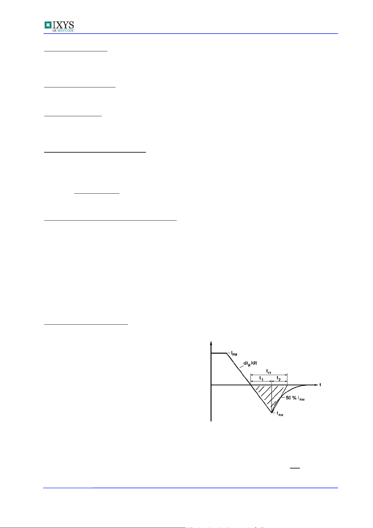
14.0 Reverse recovery ratings
(i) Q
is based on 50% Irm chord as shown in Fig. 1
ra
is based on a 50µs integration time i.e.
(ii) Q
rr
(iii)
RWT and fEW
()
.)(max
−
HsJthAVSINKPAV
Fig. 1
s
µ
150
=
rrrr
∫
0
FactorK =
dtiQ
.
1
t
2
t
Data Sheet. Types R1700MC18x & R1700MC21x Issue 2 Page 4 of 13 April 2014
 Loading...