

Distributed Gate Thyristor
Type R1280NS18# to R1280NS25#
(Old Type Number: D390CH18-25)
Absolute Maximum Ratings
Date:- 04 Mar, 2003
Data Sheet Issue:- 4
VOLTAGE RATINGS
V
DRM
V
DSM
V
RRM
V
RSM
Repetitive peak off-state voltage, (note 1) 1800-2500 V
Non-repetitive peak off-state voltage, (note 1) 1800-2500 V
Repetitive peak reverse voltage, (note 1) 1800-2100 V
Non-repetitive peak reverse voltage, (note 1) 1900-2200 V
OTHER RATINGS
I
T(AV)M
I
T(AV)M
I
T(AV)M
I
T(RMS)
I
T(d.c.)
I
TSM
I
TSM2
I2tI
I2t
(di/dt)
V
RGM
P
G(AV)
P
GM
T
j op
T
stg
Maximum average on-state current, T
Maximum average on-state current. T
Maximum average on-state current. T
Nominal RMS on-state current, T
D.C. on-state current, T
Peak non-repetitive surge tp=10ms, Vrm=0.6V
Peak non-repetitive surge tp=10ms, Vrm≤10V, (note 5)
2
t capacity for fusing tp=10ms, Vrm=0.6V
2
t capacity for fusing tp=10ms, Vrm≤10V, (note 5) 1.33×10
I
Critical rate of rise of on-state current (repetitive), (Note 6) 1000 A/µs
cr
Critical rate of rise of on-state current (non-repetitive), (Note 6) 1500 A/µs
Peak reverse gate voltage 5 V
Mean forward gate power 5 W
Peak forward gate power 30 W
Operating temperature range -40 to +125 °C
Storage temperature range -40 to +150 °C
MAXIMUM
LIMITS
MAXIMUM
LIMITS
=55°C, (note 2) 1280 A
sink
=85°C, (note 2) 851 A
sink
=85°C, (note 3) 493 A
sink
=25°C, (note 2) 2571 A
sink
=25°C, (note 4) 2123 A
sink
, (note 5) 14.8 kA
RRM
16.3 kA
, (note 5)
RRM
1.10×10
6
6
UNITS
UNITS
A2s
A2s
Notes:-
1) De-rating factor of 0.13% per °C is applicable for T
2) Double side cooled, single phase; 50Hz, 180° half-sinewave.
3) Single side cooled, single phase; 50Hz, 180° half-sinewave.
4) Double side cooled.
5) Half-sinewave, 125°C T
6) V
=67% V
D
Data Sheet. Type R1280NS18# to R1280NS25# Issue 4 Page 1 of 12 March, 2003
, IFG=2A, tr≤0.5µs, T
DRM
initial.
j
case
=125°C.
below 25°C.
j

WESTCODE
WESTCODE An IXYS Company Distributed Gate Thyristor Types R1280NS18# to R1280NS25#
WESTCODEWESTCODE
Characteristics
PARAMETER MIN. TYP. MAX. TEST CONDITIONS (Note 1) UNITS
V
TM
V
TM
V
T0
r
T
(dv/dt)crCritical rate of rise of off-state voltage 200 - - VD=80% V
I
DRM
I
RRM
V
GT
I
GT
V
GD
I
H
t
gd
t
gt
Q
rr
Q
ra
I
rm
t
rr
t
q
R
thJK
Maximum peak on-state voltage - - 2.1 ITM=2000A V
Maximum peak on-state voltage - - 2.7 ITM=3850A V
Threshold voltage - - 1.44 V
Slope resistance - - 0.33
, Linear ramp, Gate o/c
DRM
Peak off-state current - - 150 Rated V
Peak reverse current - - 150 Rated V
Gate trigger voltage - - 3.0 V
T
Gate trigger current - - 300
Gate non-trigger voltage - - 0.25 Rated V
DRM
RRM
=25°C VD=10V, IT=3A
j
DRM
mΩ
V/µs
mA
mA
mA
V
Holding current - - 1000 Tj=25°C mA
Gate controlled turn-on delay time - 0.5 1.0
Turn-on time - 1.2 2.5
=67% V
V
D
I
=2A, tr=0.5µs, Tj=25°C
FG
, ITM=1000A, di/dt=60A/µs,
DRM
µs
Recovered charge - 1200 - µC
Recovered charge, 50% Chord - 600 720 µC
Reverse recovery current - 200 - A
Reverse recovery time - 5.8 -
50 - 60
Turn-off time (note 2)
60 - 70
Thermal resistance, junction to heatsink
- - 0.022 Double side cooled K/W
I
=1000A, tp=1000µs, di/dt=60A/µs,
TM
V
=50V
r
ITM=1000A, tp=1000µs, di/dt=60A/µs,
V
=50V, Vdr=33%V
r
, dVdr/dt=20V/µs
DRM
ITM=1000A, tp=1000µs, di/dt=60A/µs,
V
=50V, Vdr=33%V
r
, dVdr/dt=200V/µs
DRM
µs
µs
- - 0.044 Single side cooled K/W
F Mounting force 19 - 26 kN
W
Weight - 510 - g
t
Notes:-
1) Unless otherwise indicated T
2) The required t
details of t
Data Sheet. Type R1280NS18# to R1280NS25# Issue 4 Page 2 of 12 March, 2003
(specified with dVdr/dt=200V/µs) is represented by a ‘#’ in the device part number. See ordering information for
q
codes.
q
=125°C.
j
WESTCODE
WESTCODE An IXYS Company Distributed Gate Thyristor Types R1280NS18# to R1280NS25#
WESTCODEWESTCODE
Notes on Ratings and Characteristics
1.0 Voltage Grade Table
Voltage Grade
V
DRM VDSM
V
V
RRM
V
V
RSM
V
V
D
DC V
V
DC V
18 1800 1800 1900 1150 1150
20 2000 2000 2100 1250 1250
21 2100 2100 2200 1300 1300
22 2200 2100 2200 1350 1300
24 2400 2100 2200 1450 1300
25 2500 2100 2200 1500 1300
2.0 Extension of Voltage Grades This report is applicable to other and higher voltage grades when supply has been agreed by Sales/Production.
3.0 Extension of Turn-off Time This Report is applicable to other tq/re-applied dv/dt combinations when supply has been agreed by Sales/Production.
4.0 Repetitive dv/dt Higher dv/dt selections are available up to 1000V/µs on request.
5.0 De-rating Factor
A blocking voltage de-rating factor of 0.13%/°C is applicable to this device for Tj below 25°C.
6.0 Snubber Components
R
When selecting snubber components, care must be taken not to use excessively large values of snubber
capacitor or excessively small values of snubber resistor. Such excessive component values may lead to
device damage due to the large resultant values of snubber discharge current. If required, please consult
the factory for assistance.
7.0 Rate of rise of on-state current
The maximum un-primed rate of rise of on-state current must not exceed 1500A/µs at any time during
turn-on on a non-repetitive basis. For repetitive performance, the on-state rate of rise of current must not
exceed 1000A/µs at any time during turn-on. Note that these values of rate of rise of current apply to the
total device current including that from any local snubber network.
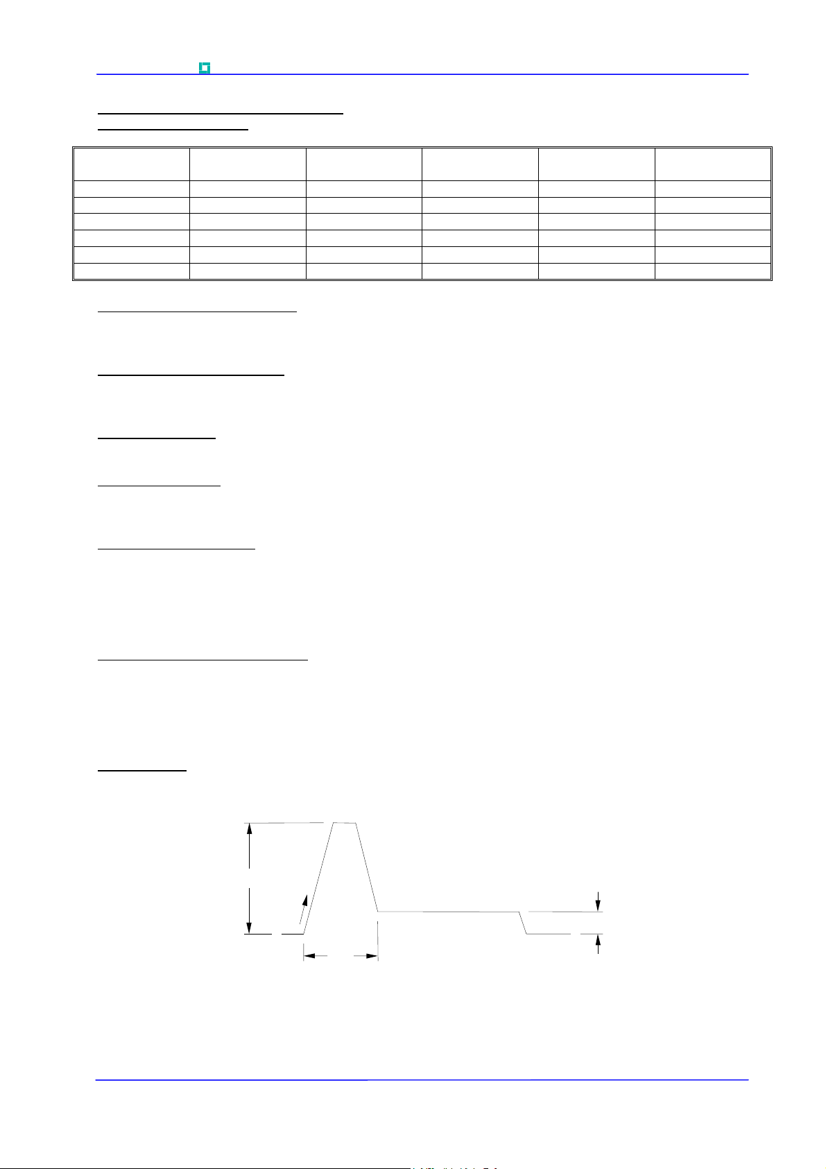
8.0 Gate Drive
The nominal requirement for a typical gate drive is illustrated below. An open circuit voltage of at least 30V
is assumed. This gate drive must be applied when using the full di/dt capability of the device.
I
GM
4A/µs
I
G
t
p1
The magnitude of IGM should be between five and ten times IGT, which is shown on page 2. Its duration
) should be 20µs or sufficient to allow the anode current to reach ten times IL, whichever is greater.
(t
p1
Otherwise, an increase in pulse current could be needed to supply the necessary charge to trigger. The
‘back-porch’ current I
magnitude in the order of 1.5 times I
should remain flowing for the same duration as the anode current and have a
G
GT
.
Data Sheet. Type R1280NS18# to R1280NS25# Issue 4 Page 3 of 12 March, 2003
WESTCODE
(
)
t
WESTCODE An IXYS Company Distributed Gate Thyristor Types R1280NS18# to R1280NS25#
WESTCODEWESTCODE
9.0 Frequency Ratings
The curves illustrated in figures 10 to 18 are for guidance only and are superseded by the maximum
ratings shown on page 1.
10.0 Square wave ratings
These ratings are given for load component rate of rise of forward current of 100 and 500 A/µs.
11.0 Duty cycle lines
The 100% duty cycle is represented on all the ratings by a straight line. Other duties can be included as
parallel to the first.
12.0 Maximum Operating Frequency
The maximum operating frequency is set by the on-state duty, the time required for the thyristor to turn off
) and for the off-state voltage to reach full value (tv), i.e.
(t
q
f
13.0 On-State Energy per Pulse Characteristics
These curves enable rapid estimation of device dissipation to be obtained for conditions not covered by
the frequency ratings.
Then the average dissipation will be:
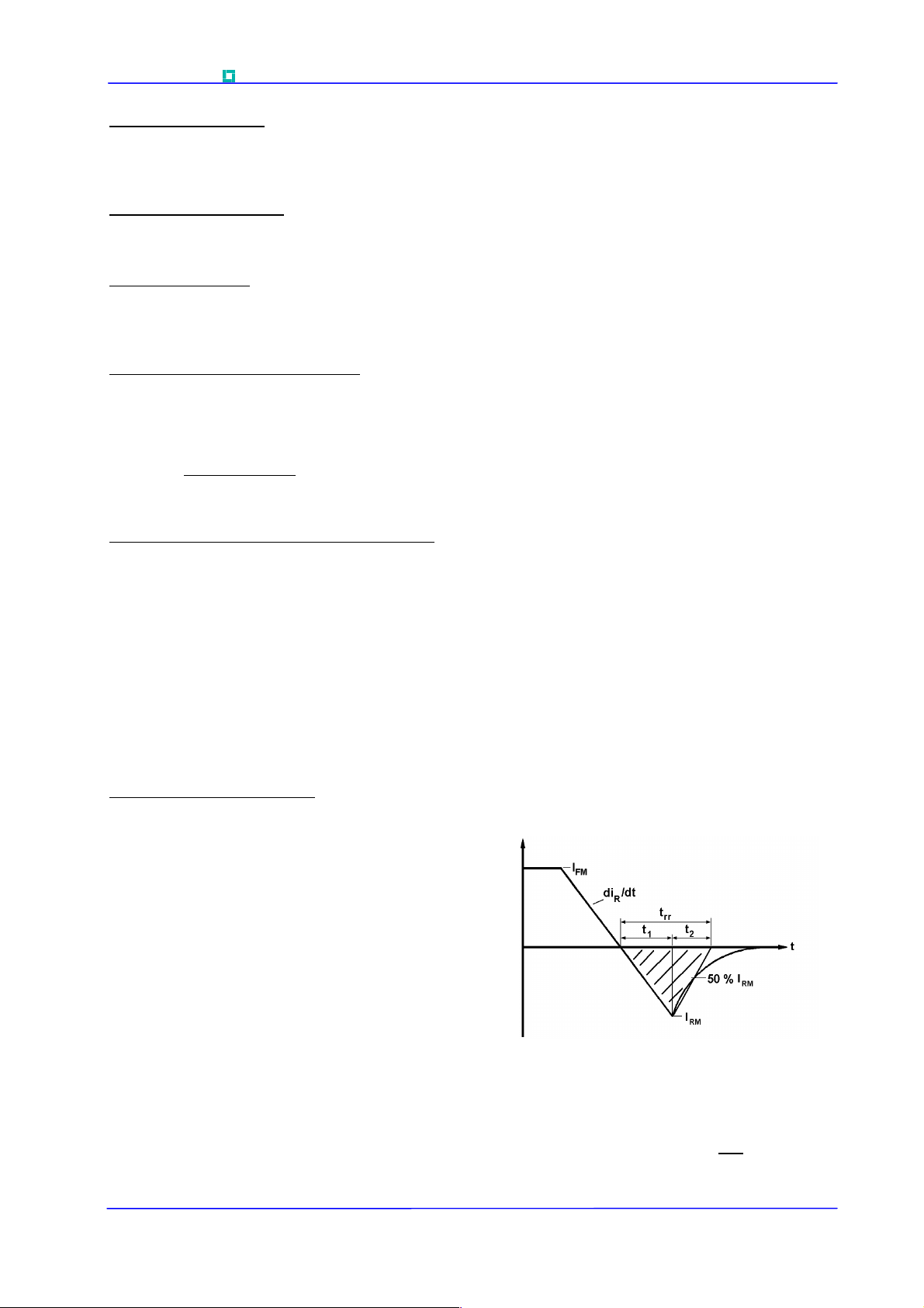
14.0 Reverse recovery ratings
(i) Qra is based on 50% Irm chord as shown in Fig. 1
=
vqpulse ttt
++
be the Energy per pulse for a given current and pulse width, in joules
Let E
p
Let R
and T
be the steady-state d.c. thermal resistance (junction to sink)
th(J-Hs)
be the heat sink temperature.
SINK
.)(max
⋅−=⋅= 125
RWT and fEW
()
HsJthAVSINKPAV
−
Fig. 1
max
1
(ii) Qrr is based on a 150µs integration time i.e.
(iii)
=
FactorK =
150
s
µ
dtiQ
.
rrrr
∫
0
t
1
2
Data Sheet. Type R1280NS18# to R1280NS25# Issue 4 Page 4 of 12 March, 2003

WESTCODE
(
)
WESTCODE An IXYS Company Distributed Gate Thyristor Types R1280NS18# to R1280NS25#
WESTCODEWESTCODE
15.0 Reverse Recovery Loss
15.1 Determination by Measurement
From waveforms of recovery current obtained from a high frequency shunt (see Note 1, Page 5) and
reverse voltage present during recovery, an instantaneous reverse recovery loss waveform must be
constructed. Let the area under this waveform be E joules per pulse. A new heat sink temperature can
then be evaluated from the following:
RfkETT
⋅+⋅−=
()
HsJthoriginalSINKnewSINK
)()(
Where k=0.227 (°C/W)/s
E = Area under reverse loss waveform per pulse in joules (W.s.)
f = rated frequency Hz at the original heat sink temperature.
= d.c. thermal resistance (°C/W).
R
th(J-Hs)
The total dissipation is now given by:
(original)(TOT)
15.2 Determination without Measurement
fEWW
⋅+=
−
In circumstances where it is not possible to measure voltage and current conditions, or for design
purposes, the additional losses E in joules may be estimated as follows.
Let E be the value of energy per reverse cycle in joules (curves in Figure 9).
Let f be the operating frequency in Hz
() ( )
Where T
T
SINK (original)
A suitable R-C snubber network is connected across the thyristor to restrict the transient reverse voltage
to a peak value (V
67% of Grade, the reverse loss may be approximated by a pro rata adjustment of the maximum value
obtained from the curves.
NOTE 1- Reverse Recovery Loss by Measurement
This thyristor has a low reverse recovered charge and peak reverse recovery current. When measuring
the charge, care must be taken to ensure that:
(a) a.c. coupled devices such as current transformers are not affected by prior passage of high
amplitude forward current.
(b) A suitable, polarised, clipping circuit must be connected to the input of the measuring oscilloscope
to avoid overloading the internal amplifiers by the relatively high amplitude forward current signal
(c) Measurement of reverse recovery waveform should be carried out with an appropriate critically
damped snubber, connected across diode anode to cathode. The formula used for the calculation
of this snubber is shown below:
SINK (new)
is the required maximum heat sink temperature and
is the heat sink temperature given with the frequency ratings.
) of 67% of the maximum grade. If a different grade is being used or Vrm is other than
rm
()
fRETT
⋅⋅−=
thoriginalSINKnewSINK
V
=
2
R
Data Sheet. Type R1280NS18# to R1280NS25# Issue 4 Page 5 of 12 March, 2003
V
C
r
di
⋅
dt
S
Where:
⋅= 4
r
C
S
R
Commutating source voltage
=
Snubber capacitance
=
Snubber resistance

WESTCODE
p
p
WESTCODE An IXYS Company Distributed Gate Thyristor Types R1280NS18# to R1280NS25#
WESTCODEWESTCODE
16.0 Computer Modelling Parameters
16.1 Calculating VT using ABCD Coefficients
The on-state characteristic I
(i) the well established V
(ii) a set of constants A, B, C, D, forming the coefficients of the representative equation for V
terms of I
The constants, derived by curve fitting software, are given in this report for hot and cold characteristics
where possible. The resulting values for V
which is limited to that plotted.
16.2 D.C. Thermal Impedance Calculation
given below:
T
vs VT, on page 7 is represented in two ways;
T
and rs tangent used for rating purposes and
0
()
agree with the true device characteristic over a current range,
T
125°C Coefficients
A 5.23269156
B -0.8154181
C -3.626×10
D 0.07016205
=
np
∑
pt
=
p
1
-5
−
t
1
−⋅=
τ
p
err
in
T
IDICIBAV ⋅+⋅+⋅+= ln
TTTT
Where p = 1 to n, n is the number of terms in the series.
t = Duration of heating pulse in seconds.
= Thermal resistance at time t.
r
t
r
= Amplitude of pth term.
= Time Constant of rth term.
τ
D.C. Single Side Cooled
Term1234
r
p
τ
p
Term 1 2 3 4
r
p
τ
p
0.0130425 6.2957×10
1.53109 0.165647 0.0207267 3.4714×10
D.C. Double Side Cooled
0.03517957 5.171738×10
6.431644 0.5234892 0.08301891 5.032106×10
-3
-3
2.35655×10
5.107098×10
-3
-3
2.23408×10
3.198402×10
-3
-3
-3
-3
Data Sheet. Type R1280NS18# to R1280NS25# Issue 4 Page 6 of 12 March, 2003

WESTCODE
WESTCODE An IXYS Company Distributed Gate Thyristor Types R1280NS18# to R1280NS25#
WESTCODEWESTCODE
Curves
Figure 1 - On-state characteristics of Limit device Figure 2 - Transient thermal impedance
(A)
T
10000
1000
R1280NS18#-25#
Issue 4
Tj = 125°C
0.1
R1280NS18#-25#
Issue 4
SSC 0.044K/W
DSC 0.022K/W
(K/W)
0.01
(th)t
Instantaneous on-state current - I
100
11.522.533.54
Instantaneous on-state voltage - V
(V)
T
0.001
Transient Thermal Impedance - Z
0.0001
0.0001 0.001 0.01 0.1 1 10 100
Time (s)
Figure 3 - Gate characteristics - Trigger limits Figure 4 - Gate characteristics - Power curves
6
Tj=25°C
5
4
(V)
GT
IGT, V
3
R1280NS18#-25#
Issue 4
Max VG dc
GT
20
18
16
14
(V)
GT
12
10
R1280NS18#-25#
Issue 4
Tj=25°C
Max VG dc
`
8
Gate Trigger Voltage - V
2
25°C
125°C
1
IGD, V
GD
0
0 0.25 0.5 0.75 1
Gate Trigger Current - I
Data Sheet. Type R1280NS18# to R1280NS25# Issue 4 Page 7 of 12 March, 2003
-10°C
GT
-40°C
Min VG dc
(A)
Gate Trigger Voltage - V
6
4
2
0
0246810
PG 5W dc
Gate Trigger Current - I
PG Max 30W dc
Min VG dc
(A)
GT

WESTCODE
WESTCODE An IXYS Company Distributed Gate Thyristor Types R1280NS18# to R1280NS25#
WESTCODEWESTCODE
Figure 5 - Total recovered charge, Q
10000
(µC)
rr
Total recovered charge - Q
R1280NS18#-25#
Issue 4
Tj = 125°C
1000
100
10 100 1000
Commutation rate - di/dt (A/µs)
rr
2000A
1500A
1000A
500A
Figure 6 - Recovered charge, Qra (50% chord)
10000
(µC)
Recovered charge - Q
R1280NS18#-25#
Issue 4
Tj = 125°C
ra
1000
100
10 100 1000
Commutation rate - di/dt (A/µs)
2000A
1500A
1000A
500A
Figure 7 - Peak reverse recovery current, I
1000
R1280NS18#-25#
Issue 4
Tj = 125°C
(A)
rm
100
Reverse recovery current - I
10
10 100 1000
Commutation rate - di/dt (A/µs)
2000A
1500A
1000A
500A
rm
Figure 8 - Maximum recovery time, trr (50% chord)
10
(µs)
rr
R1280NS18#-25#
Issue 4
Tj = 125°C
2000A
1500A
1000A
500A
Reverse recovery time - t
1
10 100 1000
Commutation rate - di/dt (A/µs)
Data Sheet. Type R1280NS18# to R1280NS25# Issue 4 Page 8 of 12 March, 2003

WESTCODE
WESTCODE An IXYS Company Distributed Gate Thyristor Types R1280NS18# to R1280NS25#
WESTCODEWESTCODE
Figure 9 – Reverse recovery energy per pulse Figure 10 - Sine wave energy per pulse
1000
R1280NS18#-25#
Issue 4
No Snubber
Tj = 125°C
Vrm = 33%V
RRM
1.00E+02
2000A
1500A
1000A
1.00E+01
R1280NS18#-25#
Issue 4
Tj=125°C
5kA
3kA
2kA
1kA
500
250A
1.00E-05 1.00E-04 1.00E-03 1.00E-02
Pulse width (s)
(mJ)
r
Energy per pulse - E
100
10 100 1000
500A
1.00E+00
Energy per pulse (J)
1.00E-01
1.00E-02
Commutation rate - di/dt (A/µs)
Figure 11 - Sine wave frequency ratings Figure 12 - Sine wave frequency ratings
1.00E+05
1.00E+04
1kA
R1280NS18#-25#
100% Duty Cycle
Issue 4
THs=55°C
1.00E+05
1.00E+04
500A
1kA
R1280NS18#-25#
Issue 4
100% Duty Cycle
THs=85°C
2kA
3kA
1.00E+03
5kA
Frequency (Hz)
1.00E+02
1.00E+01
1.00E-05 1.00E-04 1.00E-03 1.00E-02
Pulse Width (s)
Data Sheet. Type R1280NS18# to R1280NS25# Issue 4 Page 9 of 12 March, 2003
1.00E+03
Frequency (Hz)
1.00E+02
1.00E+01
2kA
3kA
5kA
1.00E-05 1.00E-04 1.00E-03 1.00E-02
Pulse width (s)

WESTCODE
WESTCODE An IXYS Company Distributed Gate Thyristor Types R1280NS18# to R1280NS25#
WESTCODEWESTCODE
Figure 13 - Square wave frequency ratings Figure 14 - Square wave frequency ratings
1.00E+05
1.00E+04
1kA
2kA
R1280NS18#-25#
Issue 4
di/dt=100A/µs
THs=55°C
100% Duty Cycle
1.00E+05
1.00E+04
500A
1kA
R1280NS18#-25#
Issue 4
di/dt=500A/µs
THs=55°C
100% Duty Cycle
3kA
1.00E+03
Frequency (Hz)
1.00E+02
1.00E+01
1.00E-05 1.00E-04 1.00E-03 1.00E-02
5kA
Pulse width (s)
1.00E+03
Frequency (Hz)
1.00E+02
1.00E+01
2kA
3kA
5kA
1.00E-05 1.00E-04 1.00E-03 1.00E-02
Pulse width (s)
Figure 15 - Square wave frequency ratings Figure 16 - Square wave frequency ratings
1.00E+05
1.00E+04
500A
1kA
R1280NS18#-25#
di/dt=100A/µs
100% Duty Cycle
Issue 4
THs=85°C
1.00E+05
1.00E+04
250A
500A
1kA
R1280NS18#-25#
Issue 4
di/dt=500A/µs
THs=85°C
100% Duty Cycle
1.00E+03
2kA
1.00E+03
Frequency (Hz)
1.00E+02
1.00E+01
1.00E-05 1.00E-04 1.00E-03 1.00E-02
Data Sheet. Type R1280NS18# to R1280NS25# Issue 4 Page 10 of 12 March, 2003
3kA
5kA
Pulse width (s)
Frequency (Hz)
1.00E+02
1.00E+01
1.00E+00
2kA
3kA
5kA
1.00E-05 1.00E-04 1.00E-03 1.00E-02
Pulse width (s)

WESTCODE
WESTCODE An IXYS Company Distributed Gate Thyristor Types R1280NS18# to R1280NS25#
WESTCODEWESTCODE
Figure 17 - Square wave energy per pulse Figure 18 - Square wave energy per pulse
1.00E+03
R1280NS18#-25#
Issue 4
di/dt=100A/µs
Tj=125°C
1.00E+03
R1280NS18#-25#
Issue 4
di/dt=500A/µs
Tj=125°C
1.00E+02
1.00E+01
5kA
3kA
1.00E+00
Energy per pulse (J)
1.00E-01
1.00E-02
2kA
1kA
500A
250A
1.00E-05 1.00E-04 1.00E-03 1.00E-02
Pulse width (s)
Figure 19 - Maximum surge and I2t Ratings
Gate may temporarily lose control of conduction angle
100000
R1280NS18#-25#
Issue 4
Tj (initial) = 125°C
(A)
TSM
I2t: V
1.00E+02
5kA
3kA
2kA
1.00E+01
1.00E+00
Energy per pulse (J)
1.00E-01
1.00E-02
1.00E-05 1.00E-04 1.00E-03 1.00E-02
Pulse width (s)
10V
≤
RRM
I2t: 60% V
RRM
1kA
500A
250A
1.00E+07
2
2
10000
I
TSM
I
TSM
: V
RRM
: 60% V
≤10V
1.00E+06
RRM
Total peak half sine surge current - I
1000
1.00E+05
135101 510 50100
Duration of surge (ms) Duration of surge (cycles @ 50Hz)
Data Sheet. Type R1280NS18# to R1280NS25# Issue 4 Page 11 of 12 March, 2003
s)
t (A
Maximum I

WESTCODE
WESTCODE An IXYS Company Distributed Gate Thyristor Types R1280NS18# to R1280NS25#
WESTCODEWESTCODE
Outline Drawing & Ordering Information
ORDERING INFORMATION (Please quote 10 digit code as below)
R1280 NS
Fixed
Type Code
Typical order code: R1280NS22M – 2200V V
IXYS Semiconductor GmbH
Edisonstraße 15
D-68623 Lampertheim
Tel: +49 6206 503-0
Fax: +49 6206 503-627
E-mail: marcom@ixys.de
IXYS Corporation
3540 Bassett Street
Santa Clara CA 95054 USA
Tel: +1 (408) 982 0700
Fax: +1 (408) 496 0670
E-mail: sales@ixys.net
The information contained herein is confidential and is protected by Copyright. The information may not be used or
disclosed except with the written permission of and in the manner permitted by the proprietors Westcode Semiconductors
Ltd.
In the interest of product improvement, Westcode reserves the right to change specifications at any ti me without prior
notice.
Devices with a suffix code (2-letter or letter/digit/letter combination) added to their generic code are not necessari ly subject
to the conditions and limits contained in this report.
Fixed
Outline Code
, 2100V V
DRM
, 70µs tq, 27.7mm clamp height capsule.
RRM
www.westcode.com
www.ixys.net
♦♦♦♦ ♦♦♦♦#
Fixed Voltage Code
V
DRM
18-25
/100
#
##
Code
t
K=60µs, L=65µs, M=70µs
Westcode Semiconductors Ltd
Langley Park Way, Langley Park,
Chippenham, Wiltshire, SN15 1GE.
E-mail: WSL.sales@westcode,com
Westcode Semiconductors Inc
Long Beach CA 90807 USA
E-mail: WSI.sales@westcode.com
q
Tel: +44 (0)1249 444524
Fax: +44 (0)1249 659448
3270 Cherry Avenue
Tel: +1 (562) 595 6971
Fax: +1 (562) 595 8182
© Westcode Semiconductors Ltd.
Data Sheet. Type R1280NS18# to R1280NS25# Issue 4 Page 12 of 12 March, 2003
 Loading...