

Date:- 22 Dec, 2005
WESTCODE
An IXYS Company
Phase Control Thyristor
Types N5946F#180 to N5946F#220
Absolute Maximum Ratings
VOLTAGE RATINGS
V
DRM
V
DSM
V
RRM
V
RSM
I
T(AV)
I
T(AV)
I
T(AV)
I
T(RMS)
I
T(d.c.)
I
TSM
I
TSM2
I2tI
I2t
(di/dt)crMaximum rate of rise of on-state current, (Note 6)
V
RGM
P
G(AV)
P
GM
T
HS
T
stg
Repetitive peak off-state voltage, (note 1) 1800-2200 V
Non-repetitive peak off-state voltage, (note 1) 1800-2200 V
Repetitive peak reverse voltage, (note 1) 1800-2200 V
Non-repetitive peak reverse voltage, (note 1) 1900-2300 V
OTHER RATINGS
Mean on-state current. T
Mean on-state current. T
Mean on-state current. T
Nominal RMS on-state current. T
D.C. on-state current. T
Peak non-repetitive surge current tp=10ms, VRM=60%V
Peak non-repetitive surge current tp=10ms, VRM≤10V, (note 5)
2
t capacity for fusing tp=10ms, VRM=60%V
2
I
t capacity for fusing tp=10ms, VRM≤10V, (note 5)
Peak reverse gate voltage 5 V
Mean forward gate power 5 W
Peak forward gate power 30 W
Operating temperature range -40 to +125 °C
Storage temperature range -40 to +150 °C
=55°C, (note 2) 5946 A
sink
=85°C, (note 2) 4073 A
sink
=85°C, (note 3) 2459 A
sink
=25°C, (note 2) 11748 A
sink
=25°C, (note 4) 10155 A
sink
RRM
, (note 5) 25.9×10
RRM
continuous, 50Hz
repetitive, 50Hz, 60s
non-repetitive
Data Sheet Issue:- 2
MAXIMUM
LIMITS
MAXIMUM
LIMITS
, (note 5) 72 kA
80 kA
6
32.0×10
6
75
150
300
UNITS
UNITS
A2s
A2s
A/µs
Notes: -
1) De-rating factor of 0.13% per °C is applicable for T
2) Double side cooled, single phase; 50Hz, 180° half-sinewave.
3) Single side cooled, single phase; 50Hz, 180° half-sinewave.
4) Double side cooled.
5) Half-sinewave, 125°C T
6) V
=67% V
D
Data Sheet. Types N5946F#180 to N5946F#220 Issue 2. Page 1 of 11 December, 2005
, ITM=1500A, IFG=2A, tr≤0.5µs, T
DRM
initial.
j
below 25°C.
j
=125°C.
case
WESTCODE An IXYS Company Phase Control Thyristor Types N5946F#180 to N5946F#220
Characteristics
PARAMETER MIN. TYP. MAX. TEST CONDITIONS (Note 1) UNITS
V
TM
V
T0
r
T
(dv/dt)crCritical rate of rise of off-state voltage 1000 - - VD=80% V
I
DRM
I
RRM
V
GT
I
GT
V
GD
I
H
t
gd
t
gt
Q
rr
Q
ra
I
rm
t
rr
t
q
R
thJK
Maximum peak on-state voltage - - 1.25 ITM=6000A V
Threshold voltage - - 0.855 V
Slope resistance - - 0.065
DRM
Peak off-state current - - 200 Rated V
Peak reverse current - - 200 Rated V
Gate trigger voltage - - 3.0 V
T
Gate trigger current - - 300
Gate non-trigger voltage - - 0.25 Rated V
DRM
RRM
=25°C, VD=10V, IT=2A
j
DRM
mΩ
V/µs
mA
mA
mA
V
Holding current - - 1000 Tj=25°C mA
Gate controlled turn-on delay time - 0.4 2.0
Turn-on time - 0.9 3.0
I
=2A, tr=0.5µs, VD=67%V
FG
I
=2000A, di/dt=10A/µs, Tj=25°C
TM
DRM
,
µs
Recovered Charge - 5800 - µC
Recovered Charge, 50% chord - 3700 5300 µC
Reverse recovery current - 140 - A
Reverse recovery time, 50% chord - 55 -
- 300 -
Turn-off time
- 500 -
Thermal resistance, junction to heatsink
- - 0.0065 Double side cooled K/W
=4000A, tp=2ms, di/dt=5A/µs, Vr=50V
I
TM
=4000A, tp=2ms, di/dt=5A/µs, Vr=50V,
I
TM
V
=67%V
dr
=4000A, tp=2ms, di/dt=5A/µs, Vr=50V,
I
TM
V
=67%V
dr
, dVdr/dt=20V/µs
DRM
, dVdr/dt=200V/µs
DRM
µs
µs
- - 0.0130 Single side cooled K/W
F Mounting force 81 - 99 Note 2 kN
W
t
Weight - 2.8 - kg
Notes: -
1) Unless otherwise indicated T
=125°C.
j
2) For other clamp forces, please consult factory
Notes on rupture rated packages.
This product is available with a non-rupture rated package.
For additional details on these products, please consult factory.
Data Sheet. Types N5946F#180 to N5946F#220 Issue 2. Page 2 of 11 December, 2005
WESTCODE An IXYS Company Phase Control Thyristor Types N5946F#180 to N5946F#220
Notes on Ratings and Characteristics
1.0 Voltage Grade Table
Voltage Grade
V
DRM VDSM VRRM
V
V
RSM
V
V
V
D
DC V
R
18 1800 1900 1150
20 2000 2100 1250
22 2200 2300 1350
2.0 Extension of Voltage Grades This report is applicable to other voltage grades when supply has been agreed by Sales/Production.
3.0 De-rating Factor A blocking voltage de-rating factor of 0.13%/°C is applicable to this device for Tj below 25°C.
4.0 Repetitive dv/dt Standard dv/dt is 1000V/µs.
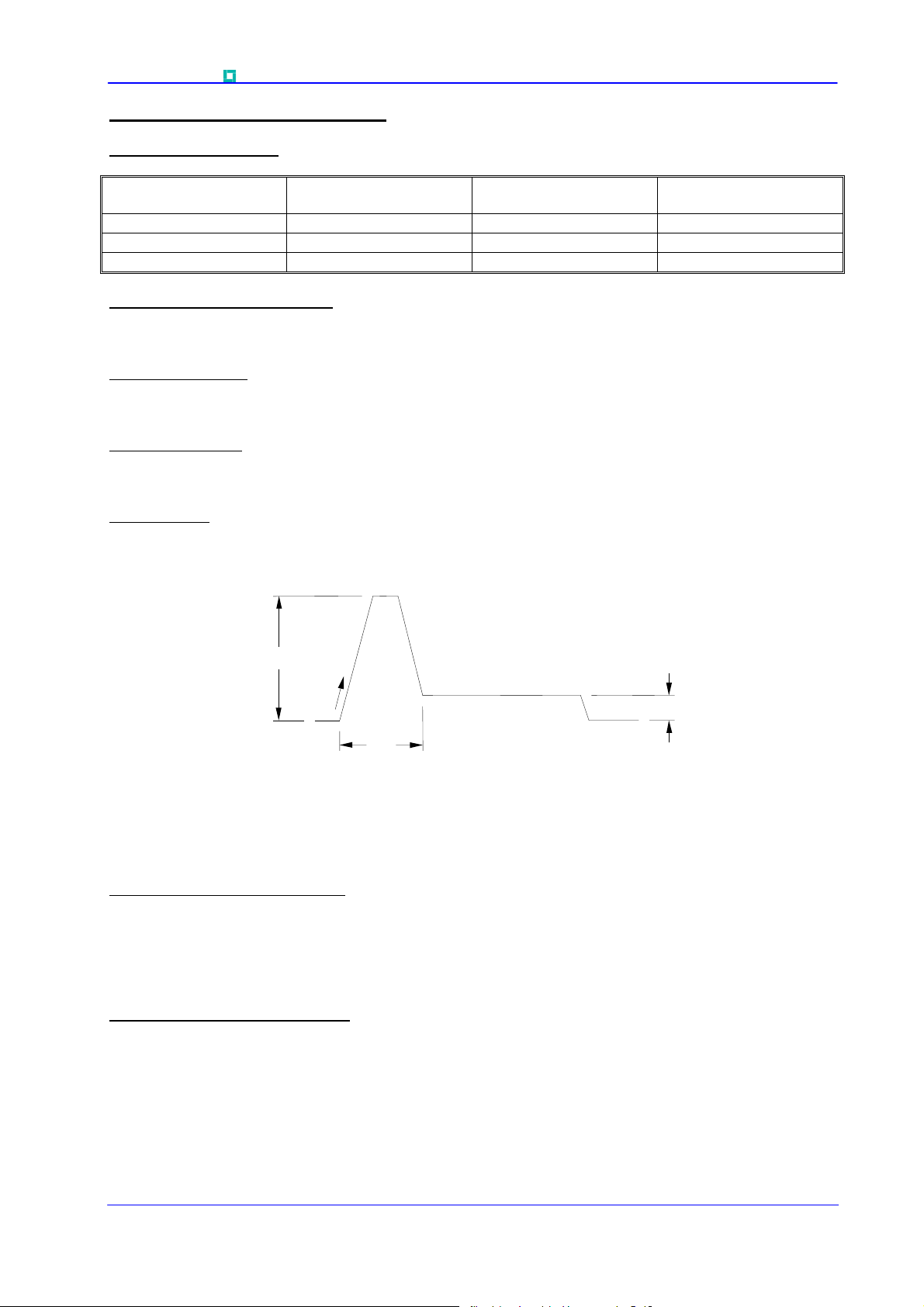
5.0 Gate Drive The nominal requirement for a typical gate drive is illustrated below. An open circuit voltage of at least
30V is assumed. This gate drive must be applied when using the full di/dt capability of the device.
I
GM
4A/µs
I
G
t
p1
The magnitude of IGM should be between five and ten times IGT, which is shown on page 2. Its duration
(t
) should be 20µs or sufficient to allow the anode current to reach ten times IL, whichever is greater.
p1
Otherwise, an increase in pulse current could be needed to supply the necessary charge to trigger. The
‘back-porch’ current I
magnitude in the order of 1.5 times I
should remain flowing for the same duration as the anode current and have a
G
.
GT
6.0 Rate of rise of on-state current The maximum un-primed rate of rise of on-state current must not exceed 1000A/µs at any time during
turn-on on a non-repetitive basis. For repetitive performance, the on-state rate of rise of current must not
exceed 500A/µs at any time during turn-on. Note that these values of rate of rise of current apply to the
total device current including that from any local snubber network.
7.0 Square wave frequency ratings These ratings are given for load component rate of rise of on-state current of 50A/µs.
Data Sheet. Types N5946F#180 to N5946F#220 Issue 2. Page 3 of 11 December, 2005
WESTCODE An IXYS Company Phase Control Thyristor Types N5946F#180 to N5946F#220
∆
p
p
8.0 Computer Modelling Parameters
8.1 Device Dissipation Calculations
2
4
I
=
AV
Where VT0=0.855, rT=0.065Ω,
R
= Supplementary thermal impedance, see table below and
th
00
2
2
2
rff
⋅⋅
T
WrffVV
⋅⋅⋅++−
AVTTT
and:
W
AV
=
R
T
th
max
TTT
−=∆
Kj
ff = Form factor, see table below.
Supplementary Thermal Impedance
Conduction Angle 30° 60° 90° 120° 180° 270° d.c.
Square wave Double Side Cooled 0.00717 0.00707 0.00698 0.00689 0.00673 0.00652 0.0065
Square wave Single Side Cooled 0.0137 0.01359 0.01349 0.0134 0.01323 0.01301 0.0130
Sine wave Double Side Cooled 0.00709 0.00697 0.00687 0.00678 0.00654
Sine wave Single Side Cooled 0.0136 0.01348 0.01337 0.01328 0.01303
Form Factors
Conduction Angle 30° 60° 90° 120° 180° 270° d.c.
Square wave 3.464 2.449 2 1.732 1.414 1.149 1
Sine wave 3.98 2.778 2.22 1.879 1.57
8.2 D.C. Thermal Impedance Calculation
−
=
np
⎛
⎜
∑
=
p
1
Where p = 1 to n, n is the number of terms in the series and:
t = Duration of heating pulse in seconds.
r
= Thermal resistance at time t.
t
r
= Amplitude of pth term.
= Time Constant of rth term.
τ
The coefficients for this device are shown in the tables below:
D.C. Double Side Cooled
Term1245
r
p
τ
p
3.424745×10
1.125391 0.1878348 0.02788979 8.430889×10
-3
1.745273×10
1
pt
⎜
⎝
-3
t
τ
p
err
−⋅=
8.532017×10
⎞
⎟
⎟
⎠
-4
3.457329×10
-4
-3
D.C. Single Side Cooled
Term1256
r
p
τ
p
Data Sheet. Types N5946F#180 to N5946F#220 Issue 2. Page 4 of 11 December, 2005
8.375269×10
8.929845 0.4711304 0.08221244 0.01221961
-3
2.518437×10
-3
1.193758×10
-3
7.45432×10
-4
WESTCODE An IXYS Company Phase Control Thyristor Types N5946F#180 to N5946F#220
(
8.3 Calculating VT using ABCD Coefficients
The on-state characteristic I
(i) the well established V
(ii) a set of constants A, B, C, D, forming the coefficients of the representative equation for V
terms of I
The constants, derived by curve fitting software, are given below for the hot and cold characteristics. The
resulting values for V
that plotted.
9.0 Snubber Components When selecting snubber components, care must be taken not to use excessively large values of snubber
capacitor or excessively small values of snubber resistor. Such excessive component values may lead to
device damage due to the large resultant values of snubber discharge current. If required, please consult
the factory for assistance.
given below:
T
T
vs. VT, on page 6 is represented in two ways;
T
and rT tangent used for rating purposes and
T0
in
T
)
agree with the true device characteristic over a current range, which is limited to
25°C Coefficients 125°C Coefficients
A 0.945893757 A 0.572724113
B -0.01897598 B 0.01470079
C 1.45867×10
D 4.798213×10
-5
-3
C 2.391723×10
D 5.239924×10
IDICIBAV ⋅+⋅+⋅+= ln
TTTT
-5
-3
10.0 Reverse recovery ratings (i) Qra is based on 50% Irm chord as shown in Fig. 1
Q
((iiii))
((iiiiii))
is based on a 150µs integration time i.e.
rr
s
µ
150
=
FactorK =
dtiQ
.
rrrr
∫
0
t
1
t
2
Fig. 1
Data Sheet. Types N5946F#180 to N5946F#220 Issue 2. Page 5 of 11 December, 2005
WESTCODE An IXYS Company Phase Control Thyristor Types N5946F#180 to N5946F#220
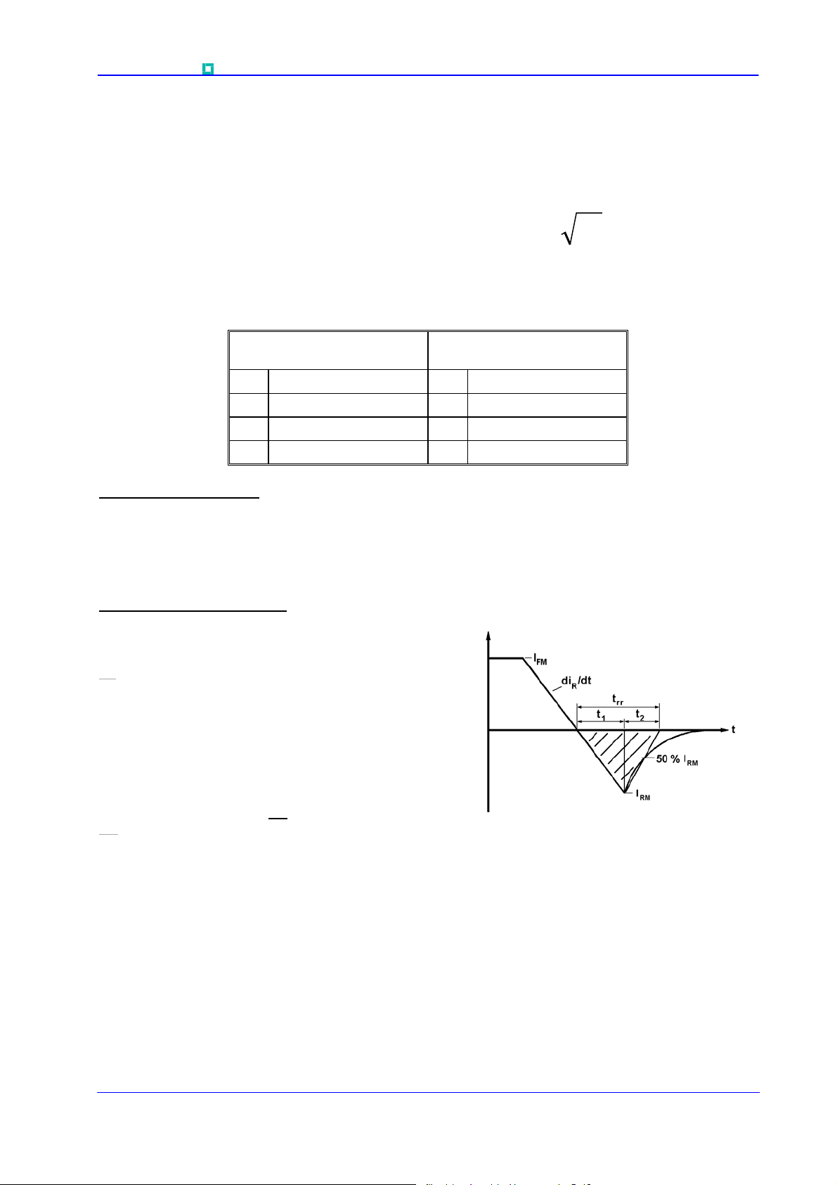
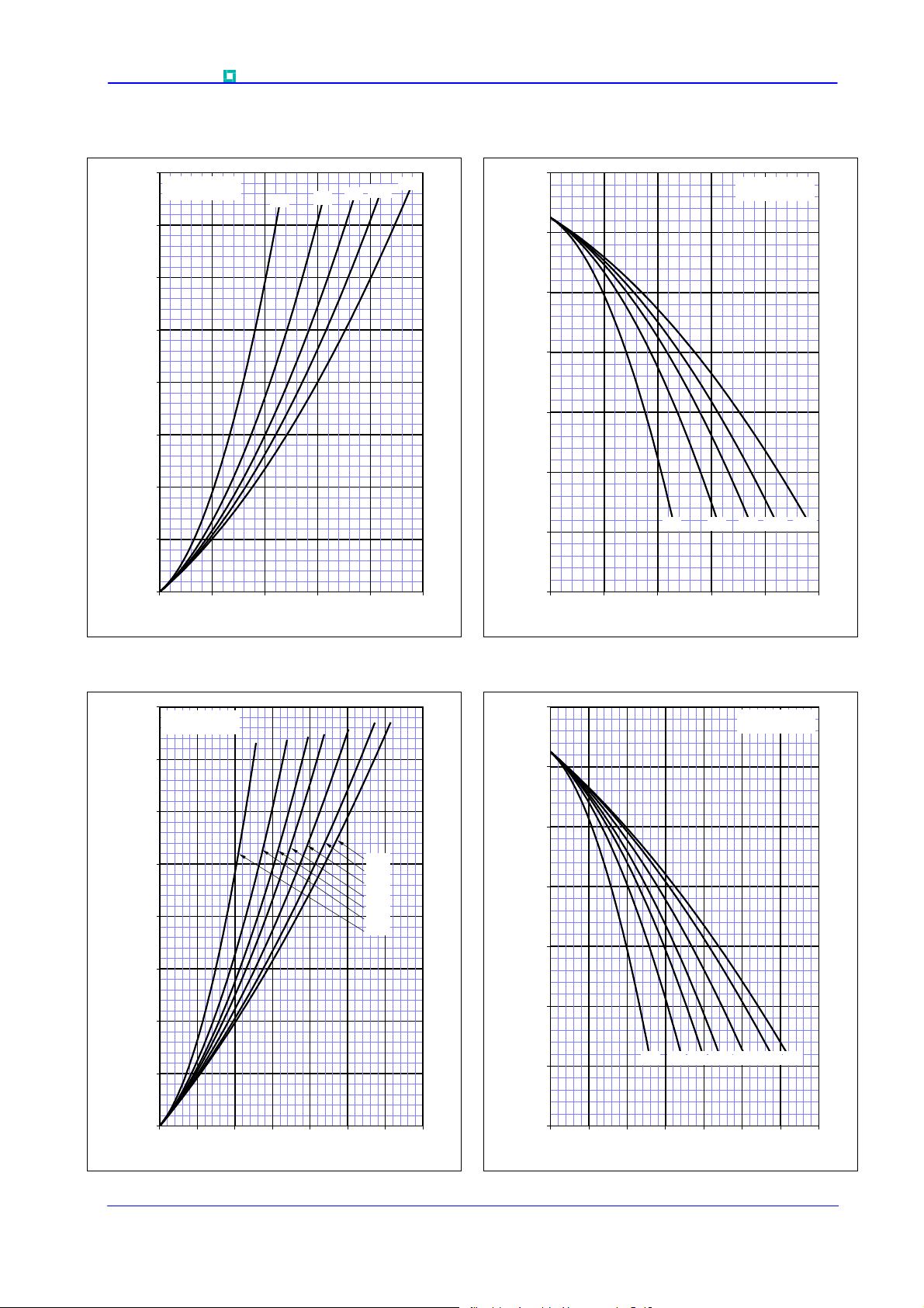
Curves
Figure 1 – On-state characteristics of Limit device Figure 2 – Transient Thermal Impedance
0.1
N5946F#180-220
Issue 2
0.01
0.001
0.0001
Transient thermal impedance (K/W)
0.00001
0.013K/W
DSC
0.0065K/W
(A)
TM
Instantaneous On-state current - I
10000
1000
N5946F#180-220
Issue 2
Tj = 25°CTj = 125°C
SSC
100
00.511.5
Instantaneous On-state voltage - V
(V)
TM
0.000001
1E-05 0.0001 0.001 0.01 0.1 1 10 100
Time (s)
Figure 3 – Gate Characteristics – Trigger Limits Figure 4 – Gate Characteristics – Power Curves
6
5
4
(V)
G
3
Gate Voltage - V
2
1
IGD, V
GD
N5946F#180-220
Issue 2
Tj=25°C
Max VG dc
IGT, V
GT
25°C
-10°C
125°C
-40°C
Min VG dc
20
N5946F#180-220
Issue 2
Tj=25°C
18
16
14
12
(V)
G
10
8
Gate Voltage - V
6
4
2
Max VG dc
PG Max 30W dc
PG 5W dc
Min VG dc
0
0 0.2 0.4 0.6 0.8 1
Gate Current - I
Data Sheet. Types N5946F#180 to N5946F#220 Issue 2. Page 6 of 11 December, 2005
(A)
G
0
0246810
Gate Current - I
(A)
G
WESTCODE An IXYS Company Phase Control Thyristor Types N5946F#180 to N5946F#220
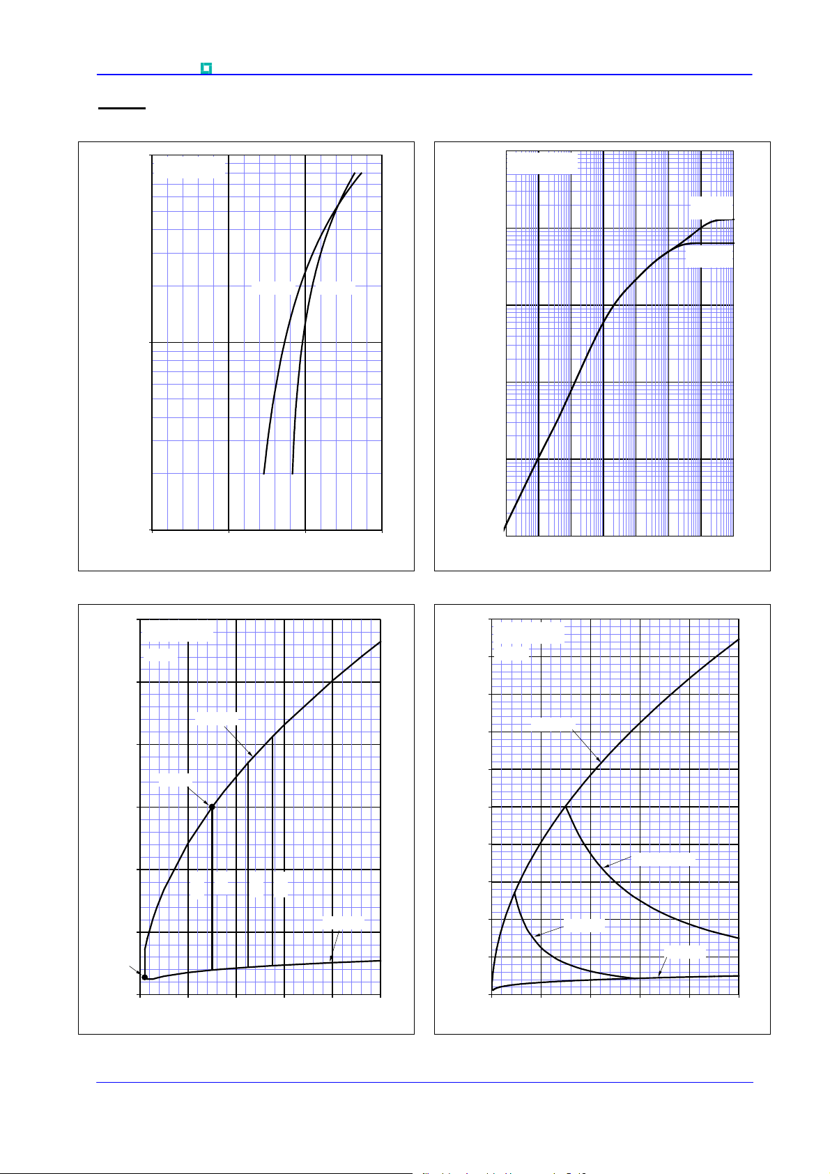
Figure 5 – Recovered Charge, Q
100000
N5946F#180-220
Issue 2
(µC)
rr
10000
Recovered charge - Q
1000
110100
di/dt (A/µs)
rr
4000A
3000A
2000A
1000A
Figure 6 – Recovered charge, Qra (50% chord)
100000
, 50% chord (µC)
ra
10000
Recovered charge - Q
1000
110100
4000A
3000A
2000A
1000A
di/dt (A/µs)
N5946F#180-220
Issue 2
Figure 7 – Reverse recovery current, I
10000
N5946F#180-220
Issue 2
1000
(A)
rm
4000A
3000A
100
Reverse recovery current - I
2000A
1000A
10
110100
di/dt (A/µs)
rm
Figure 8 – Reverse recovery time, t
100
, 50% chord (µs)
rr
Reverse recovery time - t
10
110100
di/dt (A/µs)
rr
N5946F#180-220
Issue 2
4000A
3000A
2000A
1000A
Data Sheet. Types N5946F#180 to N5946F#220 Issue 2. Page 7 of 11 December, 2005
WESTCODE An IXYS Company Phase Control Thyristor Types N5946F#180 to N5946F#220
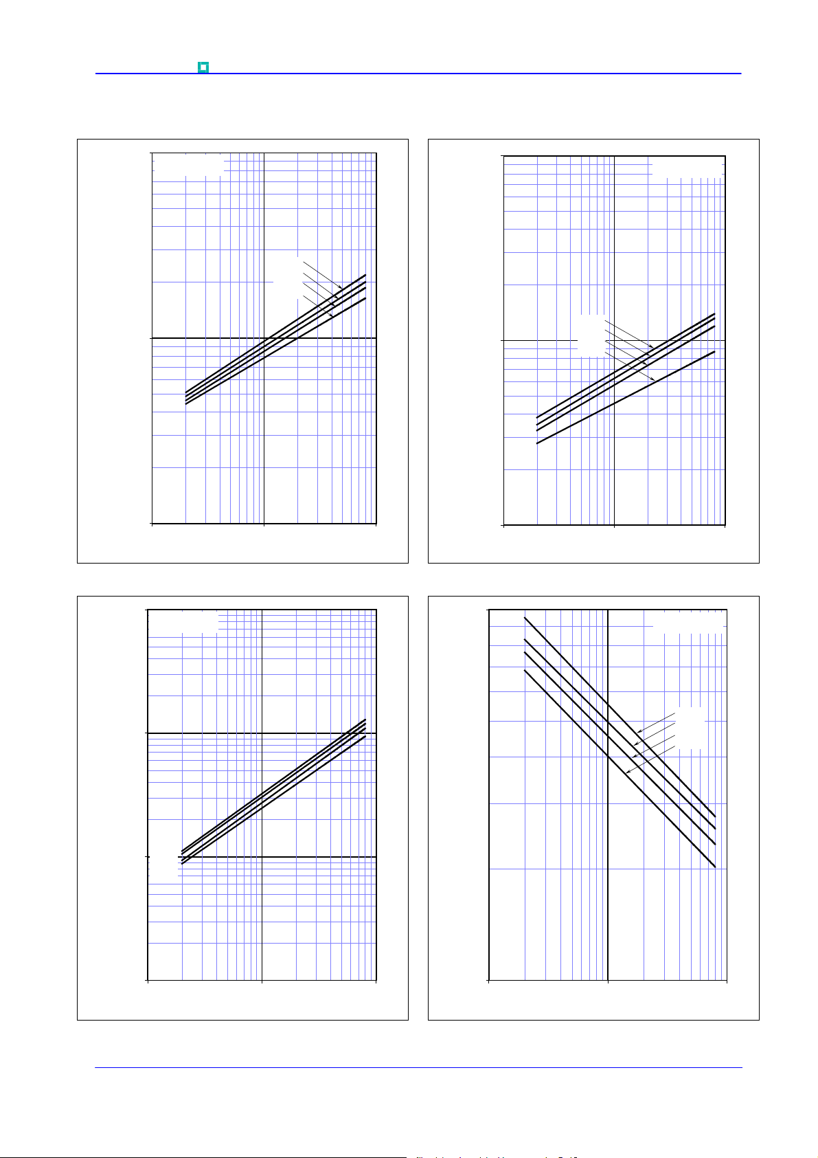
Figure 9 – On-state current vs. Power dissipation –
Double Side Cooled (Sine wave)
18000
N5946F#180-220
Issue 2
Maximum forward dissipation (W)
16000
14000
12000
10000
8000
6000
4000
2000
30°
60°
90°
120°
180°
Figure 10 – On-state current vs. Heatsink temperature
– Double Side Cooled (Sine wave)
140
120
100
80
60
40
Maximum permissable heatsink temperature (°C)
20
30° 60° 90° 120° 180°
N5946F#180-220
Issue 2
0
0 2000 4000 6000 8000
Mean forward current (A) (Whole cycle averaged)
Figure 11 – On-state current vs. Power dissipation –
Double Side Cooled (Square wave)
16000
N5946F#180-220
Issue 2
14000
12000
d.c.
10000
8000
6000
Maximum forward dissipation (W)
4000
270°
180°
120°
90°
60°
30°
0
0 2000 4000 6000 8000
Mean forward current (A) (Whole cycle averaged)
Figure 12 – On-state current vs. Heatsink temperature
– Double Side Cooled (Square wave)
140
120
100
80
60
40
Maximum permissible heatsink temperature (°C)
N5946F#180-220
Issue 2
2000
0
0 2000 4000 6000 8000 10000 12000
Mean Forward Current (A) (Whole Cycle Averaged)
Data Sheet. Types N5946F#180 to N5946F#220 Issue 2. Page 8 of 11 December, 2005
20
0
0 2000 4000 6000 8000 10000 12000
Mean Forward Current (A) (Whole Cycle Averaged)
30° 60° 90° 120° 180° d.c.270°
WESTCODE An IXYS Company Phase Control Thyristor Types N5946F#180 to N5946F#220
Figure 13 – On-state current vs. Power dissipation –
Single Side Cooled (Sine wave)
8000
7000
6000
5000
4000
3000
Maximum forward dissipation (W)
2000
1000
N5946F#180-220
Issue 2
30°
60°
90°
120°
180°
Figure 14 – On-state current vs. Heatsink temperature
– Single Side Cooled (Sine wave)
140
120
100
80
60
40
Maximum permissable heatsink temperature (°C)
20
30° 60° 90° 120° 180°
N5946F#180-220
Issue 2
0
0 1000 2000 3000 4000 5000
Mean forward current (A) (Whole cycle averaged)
Figure 15 – On-state current vs. Power dissipation –
Single Side Cooled (Square wave)
8000
N5946F#180-220
Issue 2
7000
6000
5000
4000
3000
Maximum forward dissipation (W)
2000
d.c.
270°
180°
120°
90°
60°
30°
0
0 1000 2000 3000 4000 5000
Mean forward current (A) (Whole cycle averaged)
Figure 16 – On-state current vs. Heatsink temperature
– Single Side Cooled (Square wave)
140
120
100
80
60
40
Maximum permissible heatsink temperature (°C)
N5946F#180-220
Issue 2
1000
0
0 1000 2000 3000 4000 5000 6000 7000
Mean Forward Current (A) (Whole Cycle Averaged)
Data Sheet. Types N5946F#180 to N5946F#220 Issue 2. Page 9 of 11 December, 2005
20
0
0 1000 2000 3000 4000 5000 6000 7000
Mean Forward Current (A) (Whole Cycle Averaged)
30° 60° 90° 120° 180° d.c.270°
WESTCODE An IXYS Company Phase Control Thyristor Types N5946F#180 to N5946F#220
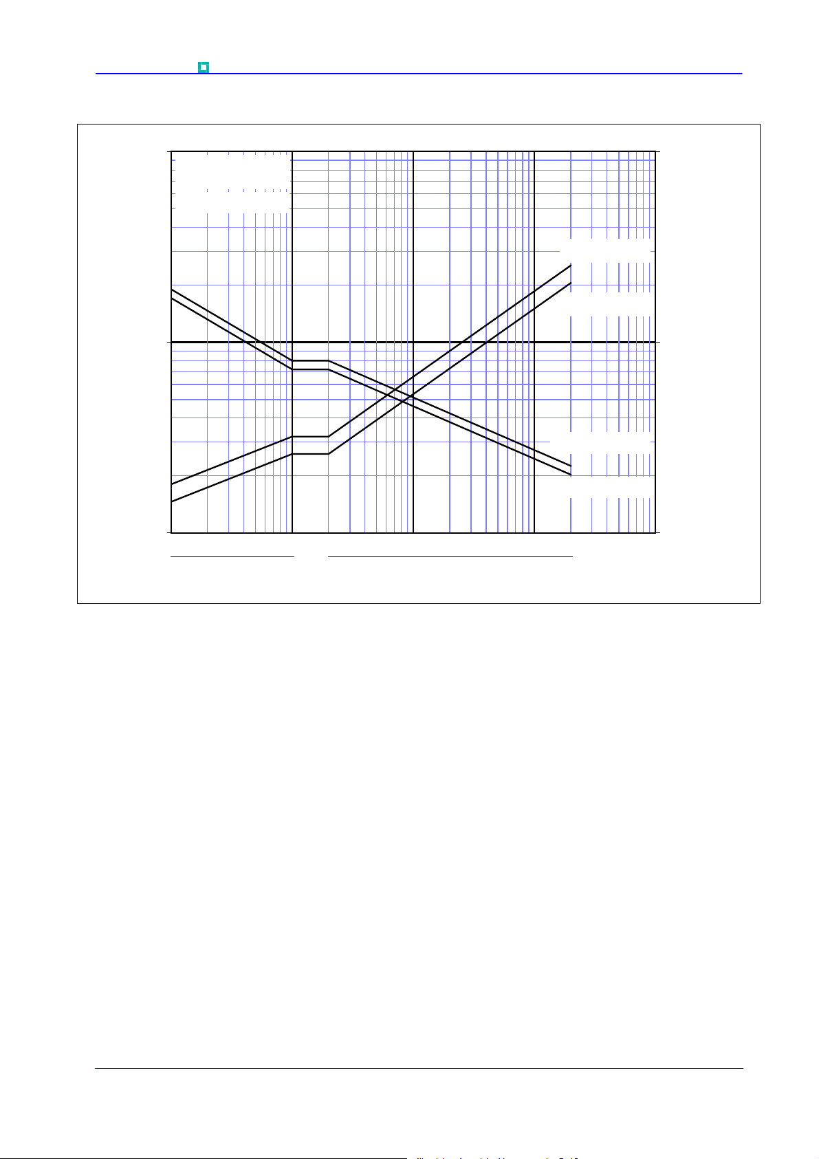
Figure 17 – Maximum surge and I2t Ratings
1000000
N5946F#180-220
Issue 2
Tj (initial) = 125°C
100000
Total peak half sine surge current (A)
10000
135101 5 10 50 100
I2t: V
I2t: 60% V
I
: V
TSM
I
: 60% V
TSM
RRM
RRM
≤
10V
RRM
≤10V
RRM
1.00E+09
1.00E+08
1.00E+07
s)
2
t (A
2
Maximum I
Duration of surge (ms) Duration of surge (cycles @ 50Hz)
Data Sheet. Types N5946F#180 to N5946F#220 Issue 2. Page 10 of 11 December, 2005
WESTCODE An IXYS Company Phase Control Thyristor Types N5946F#180 to N5946F#220
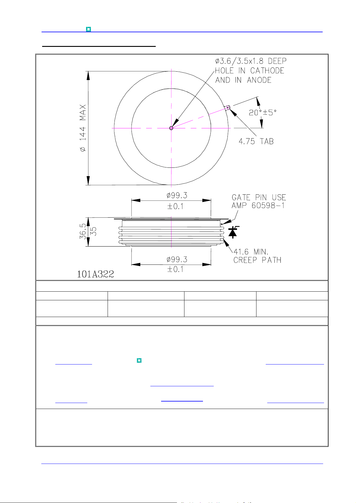
Outline Drawing & Ordering Information
ORDERING INFORMATION (Please quote 10 digit code as below)
N5946
Fixed
Type Code
Typical order code: N5946FT200 – 2000V V
IXYS Semiconductor GmbH
Edisonstraße 15
D-68623 Lampertheim
Tel: +49 6206 503-0
Fax: +49 6206 503-627
E-mail: marcom@ixys.de
IXYS Corporation
3540 Bassett Street
Santa Clara CA 95054 USA
Tel: +1 (408) 982 0700
Fax: +1 (408) 496 0670
E-mail: sales@ixys.net
The information contained herein is confidential and is protected by Copyright. The information may not be used or disclosed
except with the written permission of and in the manner permitted by the proprietors Westcode Semiconductors Ltd.
In the interest of product improvement, Westcode reserves the right to change specifications at any time without prior notice.
Devices with a suffix code (2-letter, 3-letter or letter/digit/letter combination) added to their generic code are not necessarily
subject to the conditions and limits contained in this report.
FC = Normal housing
FT = Rupture rated housing
♦♦ ♦♦
Outline code
, V
DRM
, 36mm clamp height, rupture rated capsule.
RRM
Voltage code
/100
V
RRM
18-22
WESTCODE
An IXYS Company
www.westcode.com
www.ixys.net
0
Fixed turn-off
time code
Westcode Semiconductors Ltd
Langley Park Way, Langley Park,
Chippenham, Wiltshire, SN15 1GE.
Tel: +44 (0)1249 444524
Fax: +44 (0)1249 659448
E-mail: WSL.sales@westcode.com
Westcode Semiconductors Inc
3270 Cherry Avenue
Long Beach CA 90807 USA
Tel: +1 (562) 595 6971
Fax: +1 (562) 595 8182
E-mail: WSI.sales@westcode.com
© Westcode Semiconductors Ltd.
Data Sheet. Types N5946F#180 to N5946F#220 Issue 2. Page 11 of 11 December, 2005
 Loading...