

Westcode Semiconductors N2367MK200, N2367MK220 Data Sheet
Wespack Phase Control Thyristor
Types N2367MK200 to N2367MK220
Development Type No.: NX149MK200-220
Absolute Maximum Ratings
Date:- 14th October, 2014
Data Sheet Issue:- 3
V
DRM
V
DSM
V
RRM
V
RSM
VOLTAGE RATINGS
Repetitive peak off-state voltage, (note 1) 2000-2200 V
Non-repetitive peak off-state voltage, (note 1) 2000-2200 V
Repetitive peak reverse voltage, (note 1) 2000-2200 V
Non-repetitive peak reverse voltage, (note 1) 2100-2300 V
OTHER RATINGS
I
T(AV)M
I
T(AV)M
I
T(AV)M
I
T(RMS)M
I
T(d.c.)
I
TSM
I
TSM2
I2t I2t capacity for fusing tp=10ms, Vrm=60%V
I2t
(di/dt)crCritical rate of rise of on-state current (note 6)
V
RGM
P
G(AV)
P
GM
T
j op
T
stg
Notes:-
1) De-rating factor of 0.13% per °C is applicable for T
2) Double side cooled, single phase; 50Hz, 180° half-sinewave.
3) Cathode side cooled, single phase; 50Hz, 180° half-sinewave.
4) Double side cooled.
5) Half-sinewave, 125°C T
6) V
Maximum average on-state current, T
Maximum average on-state current. T
Maximum average on-state current. T
Nominal RMS on-state current, T
D.C. on-state current, T
=25°C, (note 4) 4097 A
sink
Peak non-repetitive surge tp=10ms, Vrm=60%V
=55°C, (note 2) 2367 A
sink
=85°C, (note 2) 1644 A
sink
=85°C, (note 3) 931 A
sink
=25°C, (note 2) 4642 A
sink
, (note 5) 32.4 kA
RRM
Peak non-repetitive surge tp=10ms, Vrm≤10V, (note 5)
, (note 5) 5.25×10
RRM
2
I
t capacity for fusing tp=10ms, Vrm≤10V, (note 5)
(continuous, 50Hz) 100
(repetitive, 50Hz, 60s) 200
(non-repetitive) 400
Peak reverse gate voltage 5 V
Mean forward gate power 4 W
Peak forward gate power 30 W
Operating temperature range -40 to +125 °C
Storage temperature range -40 to +150 °C
below 25°C.
j
initial.
=67% V
D
, ITM=2000A, IFG=2A, tr≤0.5µs, T
DRM
j
=125°C.
case
MAXIMUM
LIMITS
MAXIMUM
LIMITS
UNITS
UNITS
35.7 kA
6.37×10
6
6
A2s
A2s
A/µs
Data Sheet. Types N2367MK200 to N2367MK220 Issue 3 Page 1 of 11 October, 2014

Wespack Phase Control Thyristor Types N2367MK200 to N2367MK220
Characteristics
PARAMETER MIN. TYP. MAX. TEST CONDITIONS (Note 1) UNITS
V
TM
V
TM
V
T0
r
T
(dv/dt)crCritical rate of rise of off-state voltage 1000 - - VD=80% V
I
DRM
I
RRM
V
GT
I
GT
V
GD
I
H
t
gd
t
gt
Q
rr
Q
ra
I
rr
t
rr
t
q
Maximum peak on-state voltage - - 1.50 ITM=3000A V
Maximum peak on-state voltage - - 2.40 ITM=7200A V
Threshold voltage - - 0.883 V
Slope resistance - - 0.210
, linear ramp, gate o/c
DRM
Peak off-state current - - 100 Rated V
Peak reverse current - - 100 Rated V
Gate trigger voltage - - 3.0 V
T
Gate trigger current - - 300
Gate non-trigger voltage
- - 0.25 Rated V
DRM
RRM
=25°C VD=10V, IT=3A
j
DRM
mΩ
V/µs
mA
mA
mA
V
Holding current - - 1000 Tj=25°C mA
Gate-controlled turn-on delay time - 0.8 2.0 µs
Turn-on time - 1.4 3.0
=67% V
V
D
I
=2A, tr=0.5µs, Tj=25°C
FG
, IT=2000A, di/dt=10A/µs,
DRM
µs
Recovered charge - 4000 - µC
Recovered charge, 50% Chord - 2300 2600 µC
Reverse recovery current - 155 - A
Reverse recovery time - 30 -
- 375 -
Turn-off time
- 650 -
=1000A, tp=1000µs, di/dt=10A/µs,
I
TM
V
=50V
r
=1000A, tp=1000µs, di/dt=10A/µs,
I
TM
V
=50V, Vdr=80%V
r
=1000A, tp=1000µs, di/dt=10A/µs,
I
TM
V
=50V, Vdr=80%V
r
, dVdr/dt=20V/µs
DRM
, dVdr/dt=200V/µs
DRM
µs
µs
- - 0.0140 Double side cooled K/W
R
thJK
Thermal resistance, junction to heatsink
- - 0.0253 Anode side cooled K/W
- - 0.0314 Cathode side cooled K/W
F Mounting force 25 - 31 Note 2. kN
W
t
Weight - 270 - g
Notes:-
1) Unless otherwise indicated T
2)
For other clamp forces, please consult factory.
=125°C.
j
Data Sheet. Types N2367MK200 to N2367MK220 Issue 3 Page 2 of 11 October, 2014
Wespack Phase Control Thyristor Types N2367MK200 to N2367MK220
Notes on Ratings and Characteristics
1.0 Voltage Grade Table
Voltage Grade
V
DRM VDSM VRRM
V
V
RSM
V
V
V
D
DC V
R
20 2000 2100 1250
22 2200 2300 1350
2.0 Extension of Voltage Grades This report is applicable to other voltage grades when supply has been agreed by Sales/Production.
3.0 De-rating Factor A blocking voltage de-rating factor of 0.13%/°C is applicable to this device for T
below 25°C.
j
4.0 Repetitive dv/dt Standard dv/dt is 1000V/µs.
5.0 Snubber Components When selecting snubber components, care must be taken not to use excessively large values of snubber
capacitor or excessively small values of snubber resistor. Such excessive component values may lead to
device damage due to the large resultant values of snubber discharge current. If required, please consult
the factory for assistance.
6.0 Rate of rise of on-state current The maximum un-primed rate of rise of on-state current must not exceed 400A/µs at any time during turn-
on on a non-repetitive basis. For repetitive performance, the on-state rate of rise of current must not
exceed 200A/µs at any time during turn-on. Note that these values of rate of rise of current apply to the
total device current including that from any local snubber network.
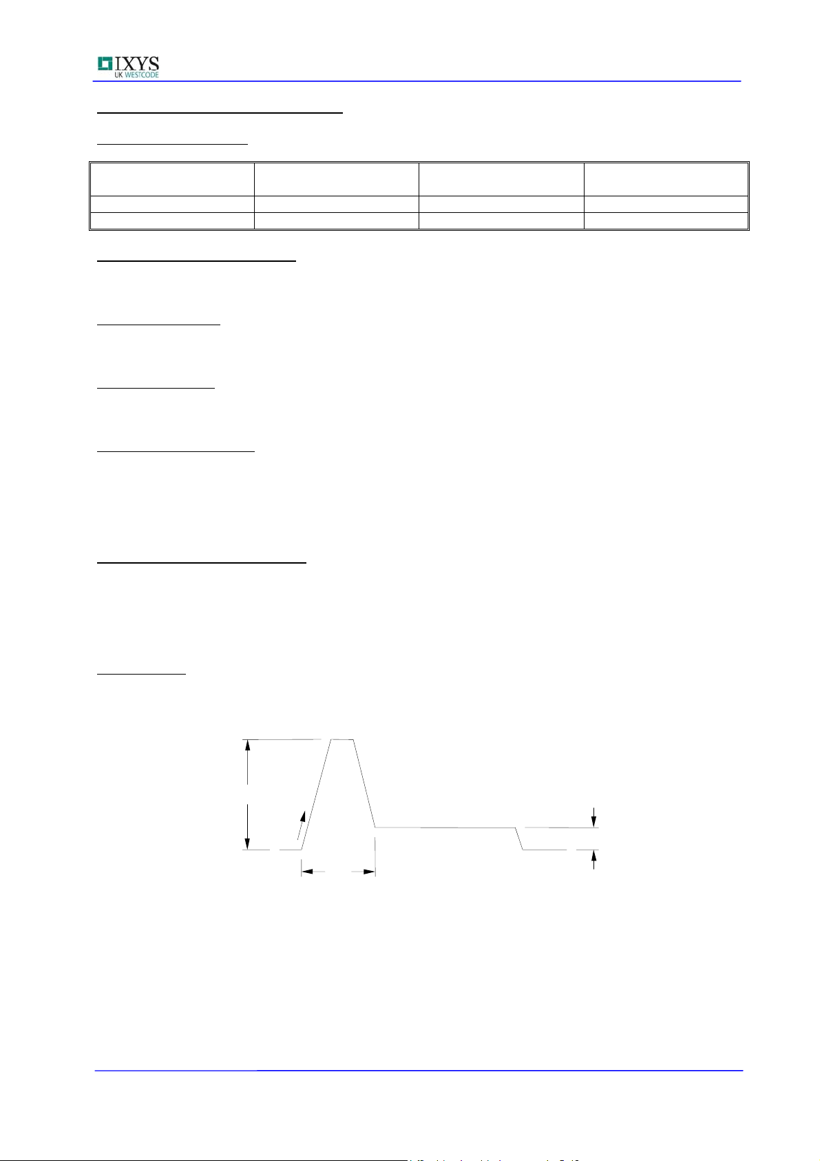
7.0 Gate Drive The nominal requirement for a typical gate drive is illustrated below. An open circuit voltage of at least
30V is assumed. This gate drive must be applied when using the full di/dt capability of the device.
I
GM
4A/µs
I
G
t
p1
The magnitude of I
) should be 20µs or sufficient to allow the anode current to reach ten times IL, whichever is greater.
(t
p1
should be between five and ten times IGT, which is shown on page 2. Its duration
GM
Otherwise, an increase in pulse current could be needed to supply the necessary charge to trigger. The
‘back-porch’ current I
magnitude in the order of 1.5 times I
should remain flowing for the same duration as the anode current and have a
G
.
GT
Data Sheet. Types N2367MK200 to N2367MK220 Issue 3 Page 3 of 11 October, 2014
Wespack Phase Control Thyristor Types N2367MK200 to N2367MK220
∆
(
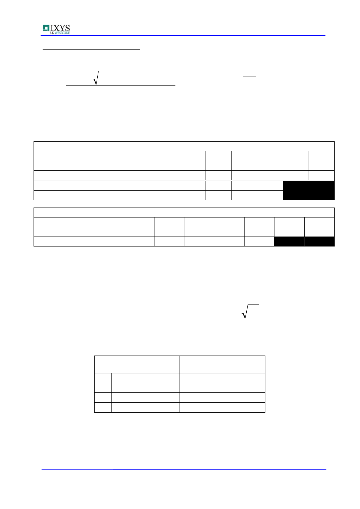
8.0 Computer Modelling Parameters
8.1 Device Dissipation Calculations
2
4
I
=
AV
Where V
R
th
=0.883V, rT=0.210mΩ,
T0
= Supplementary thermal impedance, see table below and
00
2
2
2
rff
⋅⋅
T
WrffVV
⋅⋅⋅++−
AVTTT
and:
W
AV
=
R
T
th
max
−=∆
TTT
Kj
ff = Form factor, see table below.
Supplementary Thermal Impedance
Conduction Angle 30° 60° 90° 120° 180° 270° d.c.
Square wave Double Side Cooled 0.0175 0.0168 0.0162 0.0157 0.0150 0.0143 0.0140
Square wave Cathode Side Cooled 0.0357 0.0344 0.0335 0.0329 0.0322 0.0316 0.0314
Sine wave Double Side Cooled 0.0169 0.0163 0.0158 0.0151 0.0140
Sine wave Cathode Side Cooled 0.0349 0.0340 0.0334 0.0324 0.0318
Form Factors
Conduction Angle 30° 60° 90° 120° 180° 270° d.c.
Square wave 3.46 2.45 2 1.73 1.41 1.15 1
Sine wave 3.98 2.78 2.22 1.88 1.57
8.2 Calculating V
The on-state characteristic I
(i) the well established V
(ii) a set of constants A, B, C, D, forming the coefficients of the representative equation for V
terms of I
using ABCD Coefficients
T
vs. VT, on page 6 is represented in two ways;
T
and rT tangent used for rating purposes and
T0
given below:
T
in
T
)
The constants, derived by curve fitting software, are given below for both hot and cold characteristics.
The resulting values for V
to that plotted.
Data Sheet. Types N2367MK200 to N2367MK220 Issue 3 Page 4 of 11 October, 2014
agree with the true device characteristic over a current range, which is limited
T
25°C Coefficients 125°C Coefficients
A 0.8230476 A -0.1878519
B 0.07410681 B 0.2685822
C 1.691121×10
D -7.725044×10
-4
-3
C 3.595580×10
D -0.02813815
IDICIBAV ⋅+⋅+⋅+= ln
TTTT
-4
 Loading...