

Westcode Semiconductors N1802NC120, N1802NC160 Data Sheet
Date:- 02 August 2012
Data Sheet Issue:- 2
Phase Control Thyristor
Types N1802NC120 to N1802NC160
Absolute Maximum Ratings
V
DRM
V
DSM
V
RRM
V
RSM
VOLTAGE RATINGS
Repetitive peak off-state voltage, (note 1) 1200-1600 V
Non-repetitive peak off-state voltage, (note 1) 1200-1600 V
Repetitive peak reverse voltage, (note 1) 1200-1600 V
Non-repetitive peak reverse voltage, (note 1) 1300-1700 V
OTHER RATINGS
I
Mean on-state current, T
T(AV)
I
Mean on-state current. T
T(AV)
I
Mean on-state current. T
T(AV)
I
Nominal RMS on-state current. T
T(RMS)
I
D.C. on-state current. T
T(d.c.)
I
Peak non-repetitive surge tp=10ms, VRM=0.6V
TSM
I
TSM2
I2t I2t capacity for fusing tp=10ms, VRM=0.6V
I2t
(di/dt)cr
V
RGM
P
G(AV)
PGM Peak forward gate power 30 W
VGD Non-trigger gate voltage, (Note 7) 0.25 V
THS Operating temperature range -40 to +125 °C
T
stg
Notes:-
1) De-rating factor of 0.13% per °C is applicable for T
2) Double side cooled, single phase; 50Hz, 180° half-sinewave.
3) Single side cooled, single phase; 50Hz, 180° half-sinewave.
4) Double side cooled.
5) Half-sinewave, 125°C T
6) V
7) Rated V
Peak non-repetitive surge t
2
I
t capacity for fusing tp=10ms, VRM≤10V, (note 5)
Maximum rate of rise of on-state current (repetitive), (Note 6) 500 A/µs
Maximum rate of rise of on-state current (non-repetitive), (Note 6) 1000 A/µs
Peak reverse gate voltage 5 V
Mean forward gate power 4 W
Storage temperature range -40 to +150 °C
initial.
=67% V
D
, ITM=1500A, IFG=2A, tr≤0.5µs, T
DRM
.
DRM
j
=55°C, (note 2) 1802 A
sink
=85°C, (note 2) 1216 A
sink
=85°C, (note 3) 718 A
sink
=25°C, (note 2) 3592 A
sink
= 25°C, (note 4) 3033 A
sink
, (note 5) 29.6 kA
RRM
=10ms, VRM≤10V, (note 5)
p
, (note 5) 4.38×10⁶ A
RRM
below 25°C.
j
=125°C.
case
MAXIMUM
LIMITS
MAXIMUM
LIMITS
32.5 kA
6
5.28×10
A
UNITS
UNITS
2
2
s
s
Data Sheet. Types N1802NC120 to N1802NC160 Issue 2. Page 1 of 10 August 2012
N1802NC120 to N1802NC160
Characteristics
PARAMETER MIN. TYP. MAX. TEST CONDITIONS (Note 1) UNITS
VTM
Maximum peak on-state
voltage
- - 1.29 ITM=2550A V
VT0 Threshold voltage - - 0.855 V
rT Slope resistance - - 0.171
(dv/dt)cr
I
DRM
I
RRM
Critical rate of rise of off-state
voltage
1000 - - VD=80% V
Peak off-state current - - 100 Rated V
Peak reverse current - - 100 Rated V
DRM
mA
DRM
mA
RRM
mΩ
V/µs
VGT Gate trigger voltage - - 3.0 Tj=25°C V
IGT Gate trigger current - - 300 Tj=25°C. VD=10V, IT=2A mA
IH Holding current - - 1000 Tj=25°C mA
R
thJK
Thermal resistance, junction to
heatsink
- - 0.024 Double side cooled K/W
- - 0.048 Single side cooled K/W
F Mounting force 19 - 26 kN
Wt Weight - 510 - g
Notes:-
1) Unless otherwise indicated T
=125°C.
j
Data Sheet. Types N1802NC120 to N1802NC160 Issue 2. Page 2 of 10 August 2012
N1802NC120 to N1802NC160
Notes on Ratings and Characteristics
1.0 Voltage Grade Table
Voltage Grade
V
DRM VDSM VRRM
V
V
RSM
V
VD VR
DC V
12 1200 1300 810
14 1400 1500 930
16 1600 1700 1040
2.0 Extension of Voltage Grades This report is applicable to other and higher voltage grades when supply has been agreed by
Sales/Production.
3.0 De-rating Factor A blocking voltage de-rating factor of 0.13%/°C is applicable to this device for T
below 25°C.
j
4.0 Repetitive dv/dt Standard dv/dt is 1000V/µs.
5.0 Snubber Components When selecting snubber components, care must be taken not to use excessively large values of snubber
capacitor or excessively small values of snubber resistor. Such excessive component values may lead to
device damage due to the large resultant values of snubber discharge current. If required, please consult
the factory for assistance.
6.0 Rate of rise of on-state current The maximum un-primed rate of rise of on-state current must not exceed 600A/µs at any time during turn-
on on a non-repetitive basis. For repetitive performance, the on-state rate of rise of current must not
exceed 300A/µs at any time during turn-on. Note that these values of rate of rise of current apply to the
total device current including that from any local snubber network.
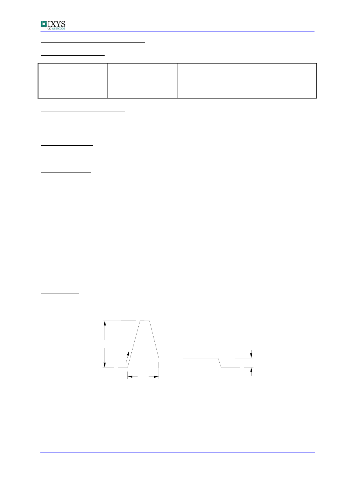
7.0 Gate Drive The nominal requirement for a typical gate drive is illustrated below. An open circuit voltage of at least
30V is assumed. This gate drive must be applied when using the full di/dt capability of the device.
I
GM
4A/µs
I
G
t
p1
The magnitude of I
) should be 20µs or sufficient to allow the anode current to reach ten times IL, whichever is greater.
(t
p1
should be between five and ten times IGT, which is shown on page 2. Its duration
GM
Otherwise, an increase in pulse current could be needed to supply the necessary charge to trigger. The
‘back-porch’ current I
magnitude in the order of 1.5 times I
should remain flowing for the same duration as the anode current and have a
G
.
GT
Data Sheet. Types N1802NC120 to N1802NC160 Issue 2. Page 3 of 10 August 2012
 Loading...