

Westcode Semiconductors N1140LN140 Data Sheet
Date:- 17th December, 2014
Data Sheet Issue:- 4
Phase Control Thyristor
VOLTAGE RATINGS
MAXIMUM
LIMITS
UNITS
V
DRM
Repetitive peak off-state voltage, (note 1)
1400
V
V
DSM
Non-repetitive peak off-state voltage, (note 1)
1500
V
V
RRM
Repetitive peak reverse voltage, (note 1)
1400
V
V
RSM
Non-repetitive peak reverse voltage, (note 1)
1500
V
OTHER RATINGS
MAXIMUM
LIMITS
UNITS
I
T(AV)M
Maximum average on-state current, T
sink
=55°C, (note 2)
1315
A
I
T(AV)M
Maximum average on-state current. T
sink
=85°C, (note 2)
930
A
I
T(AV)M
Maximum average on-state current. T
sink
=85°C, (note 3)
565
A
I
T(RMS)M
Nominal RMS on-state current, T
sink
=25°C, (note 2)
2565
A
I
T(d.c.)
D.C. on-state current, T
sink
=25°C, (note 4)
2210
A
I
TSM
Peak non-repetitive surge tp=10ms, Vrm=60%V
RRM
, (note 5)
17500
A
I
TSM2
Peak non-repetitive surge tp=10ms, Vrm10V, (note 5)
19500
A
I2t
I2t capacity for fusing tp=10ms, Vrm=60%V
RRM
, (note 5)
1.53×10⁶
A2s
I2t
I2t capacity for fusing tp=10ms, Vrm10V, (note 5)
1.90×10⁶
A2s
(di/dt)cr
Critical rate of rise of on-state current (note 6)
(continuous, 50Hz)
200
A/µs
(non-repetitive)
400
V
RGM
Peak reverse gate voltage
5
V
P
G(AV)
Mean forward gate power
3
W
PGM
Peak forward gate power
30
W
T
j op
Operating temperature range
-60 to +130
°C
T
stg
Storage temperature range
-60 to +130
°C
Absolute Maximum Ratings
Types N1140LN140
Notes:-
1) De-rating factor of 0.13% per °C is applicable for T
2) Double side cooled, single phase; 50Hz, 180° half-sinewave.
3) Single side cooled, single phase; 50Hz, 180° half-sinewave.
4) Double side cooled.
5) Half-sinewave, 130°C T
6) V
=67% V
D
Data Sheet. Types N1140LN140 Issue 4 Page 1 of 11 December, 2014
, ITM=1800A, IFG=2A, tr0.5µs, T
DRM
initial.
j
below 25°C.
j
=130°C.
case
Phase Control Thyristor Types N1140LN140
PARAMETER
MIN.
TYP.
MAX.
TEST CONDITIONS (Note 1)
UNITS
VTM
Maximum peak on-state voltage
- - 1.10
ITM=1000A
V
VTM
Maximum peak on-state voltage
- - 1.87
ITM=3765A
V
VT0
Threshold voltage
- - 0.82 V
rT
Slope resistance
- - 0.28
m
(dv/dt)cr
Critical rate of rise of off-state voltage
1000 - -
VD=67% V
DRM
, linear ramp, gate o/c
V/s
I
DRM
Peak off-state current
- - 100
Rated V
DRM
mA
I
RRM
Peak reverse current
- - 100
Rated V
RRM
mA
VGT
Gate trigger voltage
- - 2.5
Tj=25°C VD=10V, IT=3A
V
IGT
Gate trigger current
- - 250
mA
VGD
Gate non-trigger voltage
- - 0.25
Rated V
DRM
V
IH
Holding current
- - 300
Tj=25°C
mA
t
gd
Gate-controlled turn-on delay time
- - 2.0
VD=67% V
DRM
, IT=900A, di/dt=10A/µs,
IFG=2A, tr=0.5µs, Tj=25°C
µs
Qrr
Recovered charge
-
1300
1500
ITM=1000A, tp=1000µs, di/dt=10A/µs,
Vr=100V
µC
Qra
Recovered charge, 50% Chord
-
1050 - µC
Irr
Reverse recovery current
-
120 - A
t
rr
Reverse recovery time
-
18 - µs
tq
Turn-off time
-
120
230
ITM=1000A, tp=1000µs, di/dt=10A/µs,
Vr=100V, Vdr=67%V
DRM
, dVdr/dt=20V/µs
µs - 180
330
ITM=1000A, tp=1000µs, di/dt=10A/µs,
Vr=100V, Vdr=67%V
DRM
, dVdr/dt=200V/µs
µs
R
thJK
Thermal resistance, junction to heatsink
- - 0.033
Double side cooled
K/W
- - 0.066
Single side cooled
K/W
F
Mounting force
14 - 16
Note 2.
kN
Wt
Weight
-
280
- g
Characteristics
Notes:-
1) Unless otherwise indicated T
2) For other clamp forces, please consult factory.
Data Sheet. Types N1140LN140 Issue 4 Page 2 of 11 December, 2014
=130°C.
j
Phase Control Thyristor Types N1140LN140
Voltage Grade
V
DRM VRRM
V
V
DSM VRSM
V
VD VR
DC V
14
1400
1500
1050
I
GM
I
G
t
p1
4A/µs
Notes on Ratings and Characteristics
1.0 Voltage Grade Table
2.0 Extension of Voltage Grades
This report is applicable to other voltage grades when supply has been agreed by Sales/Production.
3.0 De-rating Factor
A blocking voltage de-rating factor of 0.13%/°C is applicable to this device for Tj below 25°C.
4.0 Repetitive dv/dt
Standard dv/dt is 1000V/µs.
5.0 Snubber Components
When selecting snubber components, care must be taken not to use excessively large values of snubber
capacitor or excessively small values of snubber resistor. Such excessive component values may lead to
device damage due to the large resultant values of snubber discharge current. If required, please consult
the factory for assistance.
6.0 Rate of rise of on-state current
The maximum un-primed rate of rise of on-state current must not exceed 400A/µs at any time during turn-
on on a non-repetitive basis. For repetitive performance, the on-state rate of rise of current must not
exceed 200A/µs at any time during turn-on. Note that these values of rate of rise of current apply to the
total device current including that from any local snubber network.
7.0 Gate Drive
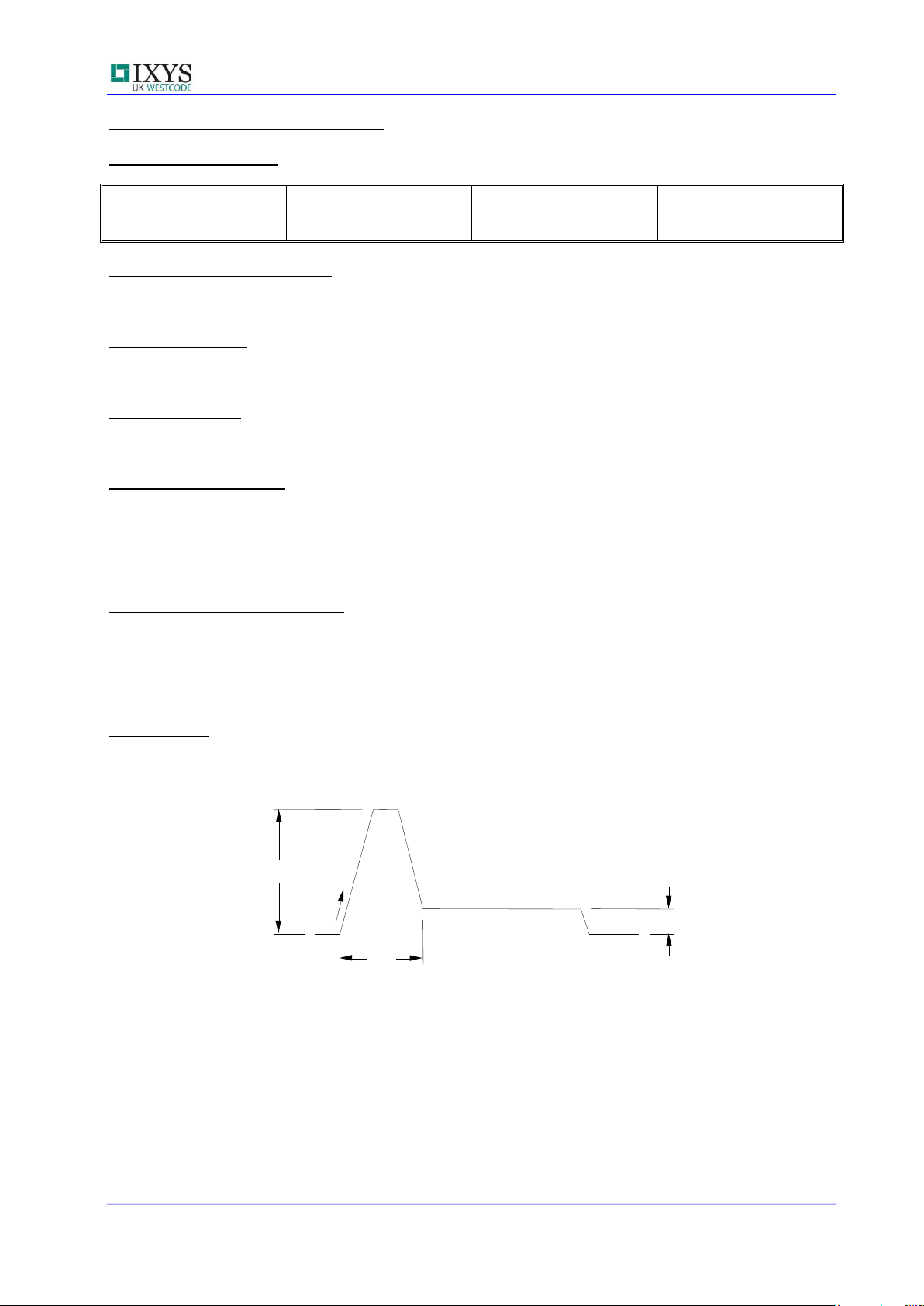
The nominal requirement for a typical gate drive is illustrated below. An open circuit voltage of at least 30V
is assumed. This gate drive must be applied when using the full di/dt capability of the device.
The magnitude of IGM should be between five and ten times IGT, which is shown on page 2. Its duration
(tp1) should be 20µs or sufficient to allow the anode current to reach ten times IL, whichever is greater.
Otherwise, an increase in pulse current could be needed to supply the necessary charge to trigger. The
‘back-porch’ current IG should remain flowing for the same duration as the anode current and have a
magnitude in the order of 1.5 times IGT.
Data Sheet. Types N1140LN140 Issue 4 Page 3 of 11 December, 2014
Phase Control Thyristor Types N1140LN140
T
AVTTT
AV
rff
WrffVV
I
2
2
2
00
2
4
Kj
th
AV
TTT
R
T
W
max
Supplementary Thermal Impedance
Conduction Angle
30°
60°
90°
120°
180°
270°
d.c.
Square wave Double Side Cooled
0.0421
0.0399
0.0383
0.0371
0.0355
0.0339
0.0330
Square wave Anode Side Cooled
0.0746
0.0720
0.0706
0.0696
0.0683
0.0671
0.0660
Sine wave Double Side Cooled
0.0401
0.0377
0.0363
0.0353
0.0331
Sine wave Anode Side Cooled
0.0718
0.0695
0.0685
0.0678
0.0664
Form Factors
Conduction Angle
30°
60°
90°
120°
180°
270°
d.c.
Square wave
3.46
2.45
2
1.73
1.41
1.15 1 Sine wave
3.98
2.78
2.22
1.88
1.57
TTTT
IDICIBAV ln
25°C Coefficients
130°C Coefficients
A
0.8686806
A
0.5478951
B
0.02859513
B
0.03900589
C
1.676531×10⁻⁴
C
2.625815×10⁻⁴
D
2.681871×10⁻⁴
D
2.506837×10⁻⁴
8.0 Computer Modelling Parameters
8.1 Device Dissipation Calculations
and:
Where VT0=0.82V, rT=0.28m
R
= Supplementary thermal impedance, see table below and
th
ff = Form factor, see table below.
8.2 Calculating VT using ABCD Coefficients
The on-state characteristic IT vs. VT, on page 6 is represented in two ways;
(i) the well established VT0 and rT tangent used for rating purposes and
(ii) a set of constants A, B, C, D, forming the coefficients of the representative equation for VT in
terms of IT given below:
The constants, derived by curve fitting software, are given below for both hot and cold characteristics. The
resulting values for VT agree with the true device characteristic over a current range, which is limited to
that plotted.
Data Sheet. Types N1140LN140 Issue 4 Page 4 of 11 December, 2014
 Loading...