

Westcode Semiconductors N1132NC300, N1132NC360 Data Sheet

Date:- 30 Jan, 2002
WESTCODE
Phase Control Thyristor
Types N1132NC300 to N1132NC360
Absolute Maximum Ratings
VOLTAGE RATINGS
V
DRM
V
DSM
V
RRM
V
RSM
I
T(AV)
I
T(AV)
I
T(AV)
I
T(RMS)
I
T(d.c.)
I
TSM
I
TSM2
I2tI
I2t
diT/dt
V
RGM
P
G(AV)
P
GM
V
GD
T
HS
T
stg
Repetitive peak off-state voltage, (note 1) 3000-3600 V
Non-repetitive peak off-state voltage, (note 1) 3000-3600 V
Repetitive peak reverse voltage, (note 1) 3000-3600 V
Non-repetitive peak reverse voltage, (note 1) 3100-3700 V
OTHER RATINGS
Mean on-state current. T
Mean on-state current. T
Mean on-state current. T
Nominal RMS on-state current. T
D.C. on-state current. T
Peak non-repetitive surge tp=10ms, VRM=0.6V
Peak non-repetitive surge tp=10ms, V
2
t capacity for fusing tp=10ms, VRM=0.6V
I2t capacity for fusing tp=10ms, V
Maximum rate of rise of on-state current (repetitive), (Note 6) 200 A/µs
Maximum rate of rise of on-state current (non-repetitive), (Note 6) 400 A/µs
Peak reverse gate voltage 5 V
Mean forward gate power 4 W
Peak forward gate power 30 W
Non-trigger gate voltage, (Note 7) 0.25 V
Operating temperature range -40 to +125 °C
Storage temperature range -40 to +150 °C
=55°C, (note 2) 1132 A
sink
=85°C, (note 2) 781 A
sink
=85°C, (note 3) 476 A
sink
=25°C, (note 2) 2228 A
sink
=25°C, (note 4) 1945 A
sink
, (note 5) 14.3 kA
RRM
≤
10V, (note 5)
RM
, (note 5) 1.02×10
RRM
≤
10V, (note 5)
RM
Data Sheet Issue:- 1
MAXIMUM
LIMITS
MAXIMUM
LIMITS
15.7 kA
6
1.23×10
6
UNITS
UNITS
A2s
A2s
Notes: -
1)
De-rating factor of 0.13% per °C is applicable for Tj below 25°C.
2)
Double side cooled, single phase; 50Hz, 180° half-sinewave.
3)
Single side cooled, single phase; 50Hz, 180° half-sinewave.
4)
Double side cooled.
5)
Half-sinewave, 125°C Tj initial.
6)
VD=67% V
7)
Rated V
Data Sheet. Types N1132NC300 to N1132NC360 Issue 1. Page 1 of 10 January, 2002
, ITM=2000A, IFG=2A, t
DRM
.
DRM
≤
0.5µs, T
r
case
=125°C.

WESTCODE
Positive development in power electronics
Characteristics
N1132NC300 to N1132NC360
PARAMETER MIN. TYP. MAX. TEST CONDITIONS
V
V
r
dv/dt Critical rate of rise of off-state voltage 1000 - - VD=80% V
I
I
V
I
I
t
t
Q
Q
I
t
t
q
R
Maximum peak on-state voltage - - 2.08 ITM=1830A V
TM
Threshold voltage - - 1.15 V
0
Slope resistance - - 0.51
S
Peak off-state current - - 100 Rated V
DRM
Peak reverse current - - 100 Rated V
RRM
Gate trigger voltage - - 3.0 V
GT
Gate trigger current - - 300
GT
Holding current - - 1000 Tj=25°C mA
H
Gate controlled turn-on delay time - 0.5 1.0
gd
Turn-on time - 1.0 2.0
gt
Recovered Charge - 4200 - µC
rr
Recovered Charge, 50% chord - 2000 2300 µC
ra
Reverse recovery current - 130 - A
rm
Reverse recovery time, 50% chord - 30 -
rr
- 400 600
Turn-off time
- 650 900
Thermal resistance, junction to
th(j-hs)
heatsink
- - 0.024 Double side cooled K/W
- - 0.048 Single side cooled K/W
T
I
FG
I
TM
I
TM
ITM=1000A, tp=1ms, di/dt=10A/µs,
V
ITM=1000A, tp=1ms, di/dt=10A/µs,
V
DRM
RRM
=25°C, VD=10V, IT=3A
j
=2A, tr=0.5µs, VD=67%V
=1000A, di/dt=10A/µs, Tj=25°C
=1000A, tp=1ms, di/dt=10A/µs, Vr=50V
=50V, Vdr=80%V
r
=50V, Vdr=80%V
r
(Note 1)
, linear ramp, gate O/C
DRM
DRM
, dVdr/dt=20V/µs
DRM
, dVdr/dt=200V/µs
DRM
,
UNITS
m
V/µs
mA
mA
mA
µs
µs
µs
F Mounting force 19 - 26 kN
W
Weight - 510 - g
t
Ω
Notes: -
Unless otherwise indicated Tj=125°C.
1)
Data Sheet. Types N1132NC300 to N1132NC360 Issue 1. Page 2 of 10 January, 2002
WESTCODE
Notes on Ratings and Characteristics
1.0 Voltage Grade Table
Positive development in power electronics
N1132NC300 to N1132NC360
V
Voltage Grade
30 3000 3100 1750
32 3200 3300 1800
34 3400 3500 1850
36 3600 3700 1900
2.0 Extension of Voltage Grades This report is applicable to other and higher voltage grades when supply has been agreed by Sales/Production.
3.0 De-rating Factor A blocking voltage de-rating factor of 0.13%/°C is applicable to this device for Tj below 25°C.
4.0 Repetitive dv/dt Standard dv/dt is 1000V/µs.
5.0 Rate of rise of on-state current The maxim um un-primed rate of ris e of on-s tate c urr ent must not exceed 400A/µs at any time during tur non on a non-repetitive basis. For repetitive performance, the on-state rate of rise of current must not exceed total device current including that from any local snubber network.
6.0 Gate Drive The recomm ended pulse gate drive is 30V, 15Ω with a short-circuit current rise time of not more than
0.5µs. This gate drive must be applied when using the full di/dt capability of the device.
200A/µs at any time during turn-on. Note that these values of rate of rise of current apply to the
DRM VDSM VRRM
V
V
RSM
V
V
V
D
DC V
R
The pulse duration may need to be configured acc ording to the application but should be no shorter than
20µs, otherwise an increase in pulse current may be needed to supply the necessary charge to trigger.
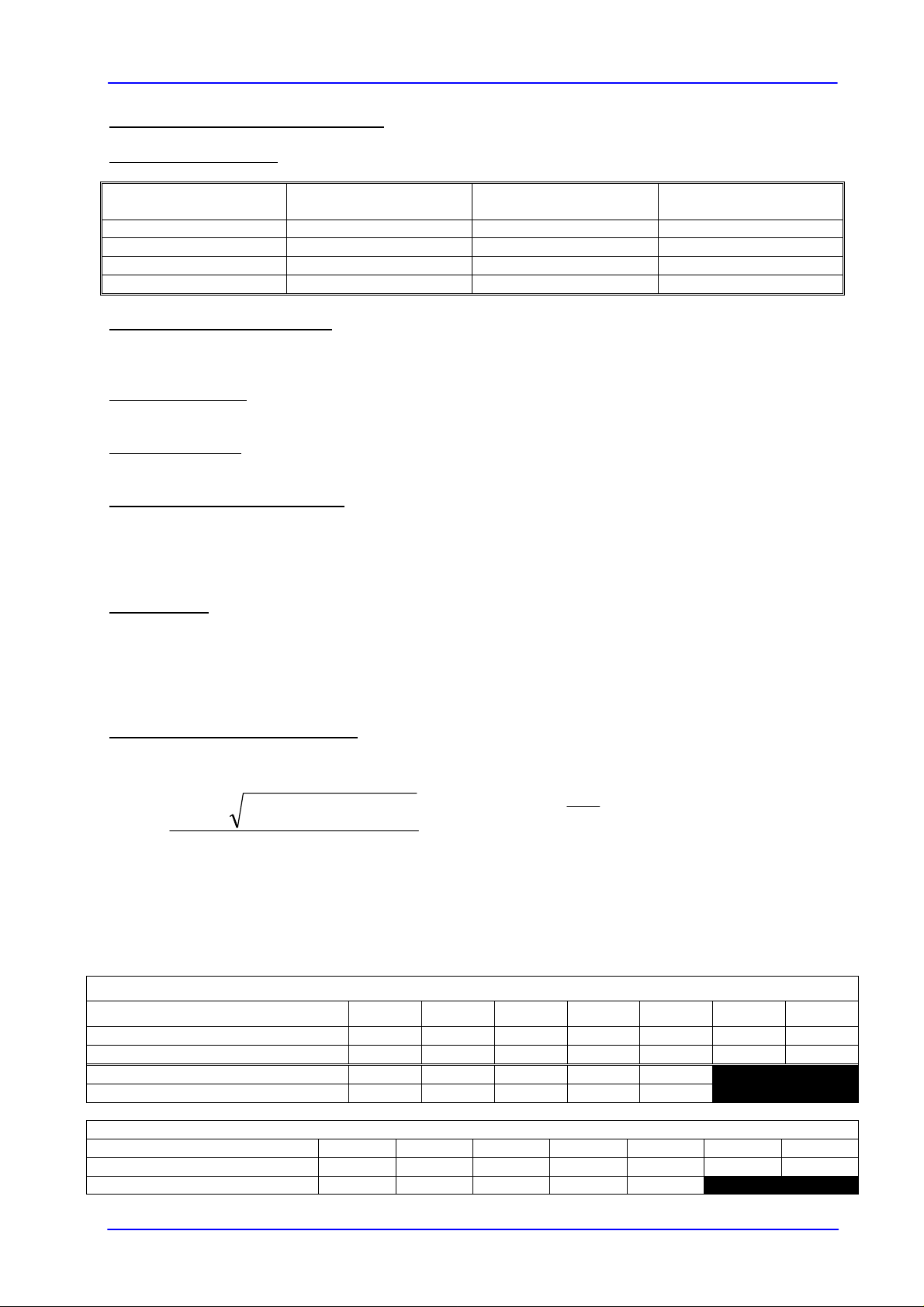
7.0 Computer Modelling Parameters
7.1 Device Dissipation Calculations
∆
2
4
=
I
AV
Where V0=1.15V, rs=0.51m
R
= Supplementary thermal impedance, see table below.
th
ff
= Form factor, see table below.
Conduction Angle 30° 60° 90° 120° 180° 270° d.c.
Square wave Double Side Cooled 0.0293 0.0285 0.0278 0.0271 0.0261 0.0249 0.024
Square wave Single Side Cooled 0.0534 0.053 0.0524 0.0518 0.0509 0.0497 0.048
Sine wave Double Side Cooled 0.0286 0.0276 0.0269 0.0263 0.0248
Sine wave Single Side Cooled 0.0531 0.0523 0.0517 0.0511 0.0497
00
⋅⋅
2
rff
Ω,
⋅⋅⋅++−
WrffVV
AVs
and:
s
Supplementary Thermal Impedance
W
AV
=
R
T
th
max
−=∆
TTT
Hsj
Form Factors
Conduction Angle 30° 60° 90° 120° 180° 270° d.c.
Square wave 3.46 2.45 2 1.73 1.41 1.15 1
Sine wave 3.98 2.78 2.22 1.88 1.57
Data Sheet. Types N1132NC300 to N1132NC360 Issue 1. Page 3 of 10 January, 2002
 Loading...