

Date:- 03 August 2012
2
Data Sheet Issue:- K1
Phase Control Thyristor
Types N0335SC120 to N0335SC160
Absolute Maximum Ratings
V
DRM
V
DSM
V
RRM
V
RSM
VOLTAGE RATINGS
Repetitive peak off-state voltage, (note 1) 1200-1600 V
Non-repetitive peak off-state voltage, (note 1) 1200-1600 V
Repetitive peak reverse voltage, (note 1) 1200-1600 V
Non-repetitive peak reverse voltage, (note 1) 1300-1700 V
OTHER RATINGS
I
Mean on-state current, T
T(AV)
I
Mean on-state current. T
T(AV)
I
Nominal RMS on-state current, T
T(RMS)
I
D.C. on-state current, T
T(d.c.)
I
Peak non-repetitive surge tp=10ms, VRM=0.6V
TSM
I
TSM2
I2t I2t capacity for fusing tp=10ms, VRM=0.6V
I2t
(di/dt)cr
V
FGM
I
FGM
V
RGM
P
G(AV)
PGM Peak forward gate power (100µs pulse width) 100 W
VGD Non-trigger gate voltage, (Note 7) 0.25 V
THS Operating temperature range -40 to +125 °C
T
stg
Notes:-
1) De-rating factor of 0.13% per °C is applicable for T
2) Double side cooled, single phase; 50Hz, 180° half-sinewave.
3) Single side cooled, single phase; 50Hz, 180° half-sinewave.
4) Double side cooled.
5) Half-sinewave, 125°C T
6) V
7) Rated V
Peak non-repetitive surge tp=10ms, VRM≤10V, (note 5)
I2t capacity for fusing tp=10ms, VRM≤10V, (note 5)
Maximum rate of rise of on-state current (repetitive), (Note 6) 500 A/µs
Maximum rate of rise of on-state current (non-repetitive), (Note 6) 1000 A/µs
Peak forward gate voltage 18 V
Peak forward gate current 20 A
Peak reverse gate voltage 5 V
Mean forward gate power 2 W
Storage temperature range -40 to +150 °C
initial.
=80% V
D
, IFG=1A, tr≤1µs, T
DRM
.
DRM
j
=55°C, (note 2) 335 A
sink
=85°C, (note 2) 226 A
sink
=25°C, (note 2) 355 A
sink
=25°C, (note 4) 355 A
sink
, (note 5) 4650 A
RRM
, (note 5) 108×103 A
RRM
below 25°C.
j
=125°C.
case
MAXIMUM
LIMITS
MAXIMUM
LIMITS
5120 A
131×103 A
UNITS
UNITS
2
s
s
Data Sheet. Types N0335SC120-160 Issue K1 Page 1 of 9 August 2012
Phase control thyristor types N0335SC120-160
Characteristics
PARAMETER MIN. TYP. MAX. TEST CONDITIONS (Note 1) UNITS
VTM Maximum peak on-state voltage - - 1.62 ITM=710A V
VT0 Threshold voltage - - 0.92 V
rT Slope resistance - - 0.99
(dv/dt)cr Critical rate of rise of off-state voltage 200 - - VD=80% V
I
Peak off-state current - - 20 Rated V
DRM
I
Peak reverse current - - 20 Rated V
RRM
DRM
mA
DRM
mA
RRM
VGT Gate trigger voltage - - 3.0 Tj=25°C V
IGT Gate trigger current - - 150 Tj=25°C VD=6V, IT=1A mA
IH Holding current - - 600 Tj=25°C mA
R
thJC
Thermal resistance, junction to case - - 0.12 Double side cooled K/W
F Mounting torque 24.5 - 27 Nm
Wt Weight - 280 - g
Notes:-
1) Unless otherwise indicated T
=125°C.
j
mΩ
V/µs
Data Sheet. Types N0335SC120-160 Issue K1 Page 2 of 9 August 2012
Phase control thyristor types N0335SC120-160
Notes on Ratings and Characteristics
1.0 Voltage Grade Table
Voltage Grade
V
DRM VDSM VRRM
V
V
RSM
V
VD VR
DC V
12 1200 1300 810
14 1400 1500 930
16 1600 1700 1040
2.0 Extension of Voltage Grades This report is applicable to other voltage grades when supply has been agreed by Sales/Production.
3.0 De-rating Factor A blocking voltage de-rating factor of 0.13%/°C is applicable to this device for T
below 25°C.
j
4.0 Repetitive dv/dt Standard dv/dt is 1000V/µs.
5.0 Snubber Components When selecting snubber components, care must be taken not to use excessively large values of snubber
capacitor or excessively small values of snubber resistor. Such excessive component values may lead to
device damage due to the large resultant values of snubber discharge current. If required, please consult
the factory for assistance.
6.0 Rate of rise of on-state current The maximum un-primed rate of rise of on-state current must not exceed 1000A/µs at any time during
turn-on on a non-repetitive basis. For repetitive performance, the on-state rate of rise of current must not
exceed 500A/µs at any time during turn-on. Note that these values of rate of rise of current apply to the
total device current including that from any local snubber network.
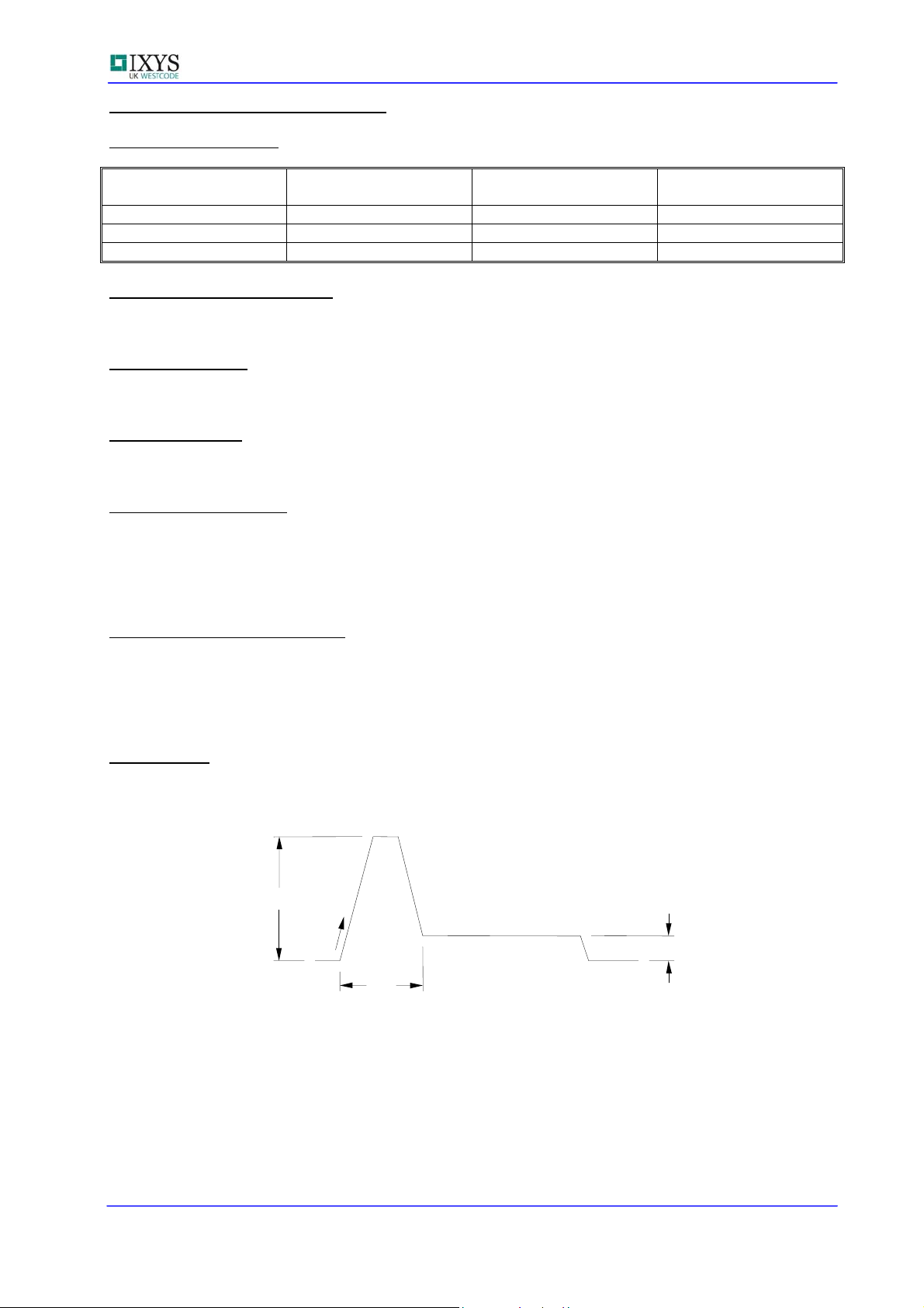
7.0 Gate Drive The nominal requirement for a typical gate drive is illustrated below. An open circuit voltage of at least
30V is assumed. This gate drive must be applied when using the full di/dt capability of the device.
I
GM
4A/µs
I
G
t
p1
The magnitude of I
(t
) should be 20µs or sufficient to allow the anode current to reach ten times IL, whichever is greater.
p1
should be between five and ten times IGT, which is shown on page 2. Its duration
GM
Otherwise, an increase in pulse current could be needed to supply the necessary charge to trigger. The
‘back-porch’ current I
magnitude in the order of 1.5 times I
should remain flowing for the same duration as the anode current and have a
G
.
GT
Data Sheet. Types N0335SC120-160 Issue K1 Page 3 of 9 August 2012

Phase control thyristor types N0335SC120-160
Curves
Figure 1 - On-state characteristics of Limit device
Figure 2 - Transient thermal impedance
Data Sheet. Types N0335SC120-160 Issue K1 Page 4 of 9 August 2012

Phase control thyristor types N0335SC120-160
Figure 3 - Gate characteristics at 25°C junction temperature
Figure 4 - Gate trigger characteristic
Trigger point of all thyristors lie within the areas shown.
Gate drive load line must lie outside appropriate I
G/VG
rectangle
Data Sheet. Types N0335SC120-160 Issue K1 Page 5 of 9 August 2012

Phase control thyristor types N0335SC120-160
Figure 5 – On-state current vs. case temperature - (Sine wave)
Mean on-state current (A)
Figure 6 - On-state current vs. Power dissipation - (Sine wave)
Data Sheet. Types N0335SC120-160 Issue K1 Page 6 of 9 August 2012

Phase control thyristor types N0335SC120-160
Figure 7 – On-state current vs. case temperature - (Square wave)
Mean on-state current (A)
Figure 8 – On-state current vs. Power dissipation - (Square wave)
Data Sheet. Types N0335SC120-160 Issue K1 Page 7 of 9 August 2012

Phase control thyristor types N0335SC120-160
Figure 9 – Maximum surge and I2t Ratings
Data Sheet. Types N0335SC120-160 Issue K1 Page 8 of 9 August 2012

Phase control thyristor types N0335SC120-160
Outline Drawing & Ordering Information
101A225
ORDERING INFORMATION (Please quote 10 digit code as below)
N0335 SC
Fixed
Type Code
Typical order code: N0335SC140 – 1400V V
IXYS Semiconductor GmbH
Edisonstraße 15
D-68623 Lampertheim
Tel: +49 6206 503-0
Fax: +49 6206 503-627
E-mail: marcom@ixys.de
IXYS Corporation
1590 Buckeye Drive
Milpitas CA 95035-7418
Tel: +1 (408) 457 9000
Fax: +1 (408) 496 0670
E-mail: sales@ixys.net
The information contained herein is confidential and is protected by Copyright. The information may not be used or
disclosed except with the written permission of and in the manner permitted by the proprietors IXYS UK Westcode Ltd.
In the interest of product improvement, IXYS UK Westcode Ltd reserves the right to change specifications at any time
without prior notice.
Devices with a suffix code (2-letter or letter/digit/letter combination) added to their generic code are not necessarily subject
to the conditions and limits contained in this report.
Fixed
Outline Code
RRM/VDRM
www.ixysuk.com
www.ixys.com
Off-state Voltage Code
♦ ♦
V
DRM
12-16
/100
0
Fixed Code
IXYS UK Westcode Ltd
Langley Park Way, Langley Park,
Chippenham, Wiltshire, SN15 1GE.
Tel: +44 (0)1249 444524
Fax: +44 (0)1249 659448
E-mail: sales@ixysuk.com
IXYS Long Beach
IXYS Long Beach, Inc
2500 Mira Mar Ave, Long Beach
CA 90815
Tel: +1 (562) 296 6584
Fax: +1 (562) 296 6585
E-mail: service@ixyslongbeach.com
© IXYS UK Westcode Ltd.
Data Sheet. Types N0335SC120-160 Issue K1 Page 9 of 9 August 2012
 Loading...