

EVALUATION LABORATORY
Rating Report
Origin
Issue 2
-
PAR 985
-
Date
Total Pages
23 July, 2004
-
13
-
Fast Recovery Diode
Types M2408N#020 to M2408N#060
Old Type No.: SM02-06CXC504
Author EL Check/Approval QA Approval S & M Approval
N. A. Tarling
Abstract
The M2408N#020-060 fast recovery diode consists of a 50mm diameter silicon slice (manufacturing
reference FFA), mounted in a cold weld caps ule. It has soft recovery characteristics and low values of
stored charge.
Summary of changes to previous issue.
Issue 1
Issue 2 Addition of ‘D’ Housing option (21mm Clamp height)
The information contained herein is confidential and is protected by Copyright. The information may not be
used or disclosed except with the written permis sion of and in the manner permitted by the propr ietors
Westcode Semiconductors Ltd.
In the interest of product im provement, W estcode res erves the right to change specif ications at any time
without prior notice.
Devices with a suffix code (2-letter, 3-letter or letter/digit/letter combination) added to their generic code
are not necessarily subject to the conditions and limits contained in this report.
First issue – Device T
Previous Datasheet M1825NC020-060 (June 2004) is now obsolete
uprated to 150°C. All ratings reflect this change.
JMAX
Rating Report. Types M2408N#020 to M2408N#060 Issue 2 Page i July, 2004

Contents
Abstract......................................................................................................................................................... i
Contents.......................................................................................................................................................ii
Absolute Maximum Ratings....................................................................................................................... 1
Characteristics ............................................................................................................................................2
Notes on Ratings and Characteristics......................................................................................................3
1.0 Voltage Grade Table ........................................................................................................................... 3
2.0 De-rating Factor...................................................................................................................................3
3.0 ABCD Constants ................................................................................................................................. 3
4.0 Reverse recovery ratings.....................................................................................................................3
5.0 Reverse Recovery Loss ......................................................................................................................4
NOTE 1 - Reverse Recovery Loss by Measurement...............................................................................................................4
6.0 Snubber Components.......................................................................................................................... 4
7.0 Computer Modelling Parameters.........................................................................................................5
7.1 Device Dissipation Calculations.........................................................................................................................................5
7.2 Calculation of V
using ABCD Coefficients.......................................................................................................................5
F
8.0 Frequency Ratings...............................................................................................................................5
9.0 Square wave ratings............................................................................................................................ 5
10.0 Duty cycle lines.................................................................................................................................. 5
Curves..........................................................................................................................................................6
Figure 1 – Forward characteristics of Limit device.................................................................................... 6
Figure 2 – Maximum forward recovery voltage .........................................................................................6
Figure 3 - Recovered charge, Q
Figure 4 - Recovered charge, Q
Figure 5 - Maximum reverse current, I
Figure 6 - Maximum recovery time, t
..............................................................................................................6
rr
(50% chord)......................................................................................... 6
ra
...................................................................................................7
rm
(50% chord)................................................................................... 7
rr
Figure 7 – Reverse recovery energy per pulse..........................................................................................7
Figure 8 - Sine wave energy per pulse...................................................................................................... 7
Figure 9 - Sine wave frequency vs. pulse width, 55°C heatsink................................................................ 8
Figure 10 - Sine wave frequency vs. pulse width, 85°C heatsink.............................................................. 8
Figure 11 - Square wave energy per pulse, 100A/µs................................................................................ 8
Figure 12 - Square wave energy per pulse, 500A/µs................................................................................ 8
Figure 13 - Square wave frequency vs. pulse width, 55°C heatsink, 100A/µs.......................................... 9
Figure 14 - Square wave frequency vs. pulse width, 55°C heatsink, 500A/µs.......................................... 9
Figure 15 - Square wave frequency vs. pulse width, 85°C heatsink, 100A/µs.......................................... 9
Figure 16 - Square wave frequency vs. pulse width, 85°C heatsink, 500A/µs.......................................... 9
Figure 17 – Maximum surge and I
2
t ratings.............................................................................................10
Figure 18 – Transient thermal impedance............................................................................................... 10
Outline Drawing & Ordering Information................................................................................................11
Rating Report. Types M2408N#020 to M2408N#060 Issue 2 Page ii July, 2004

Date:- 23 Jul, 2004
WESTCODE
An IXYS Company
Fast Recovery Diode
Type M2408N#020 to M2408N#060
Old Type No.: SM02-06CXC504
Absolute Maximum Ratings
VOLTAGE RATINGS
V
RRM
V
RSM
I
F(AV)M
I
F(AV)M
I
F(AV)M
I
F(RMS)
I
F(d.c.)
I
FSM
I
FSM2
I2tI
I2t
T
j op
T
stg
Repetitive peak reverse voltage, (note 1) 200-600 V
Non-repetitive peak reverse voltage, (note 1) 300-700 V
OTHER RATINGS
Maximum average forward current, T
Maximum average forward current. T
Maximum average forward. T
Nominal RMS forward current, T
D.C. forward current, T
Peak non-repetitive surge tp=10ms, VRM=60%V
Peak non-repetitive surge tp=10ms, VRM≤10V, (note 5)
2
t capacity for fusing tp=10ms, VRM=60%V
2
I
t capacity for fusing tp=10ms, VRM≤10V, (note 5)
Operating temperature range -40 to +150 °C
Storage temperature range -40 to +150 °C
sink
=100°C, (note 3) 857 A
sink
=25°C, (note 4) 3736 A
=55°C, (note 2) 2408 A
sink
=100°C, (note 2) 1497 A
sink
=25°C, (note 2) 4585 A
sink
, (note 5) 24.0 kA
RRM
, (note 5) 2.88×10
RRM
Data Sheet Issue:- 1
MAXIMUM
LIMITS
MAXIMUM
LIMITS
26.4 kA
6
3.48×10
6
UNITS
UNITS
A2s
A2s
Notes:-
1) De-rating factor of 0.13% per °C is applicable for T
2) Double side cooled, single phase; 50Hz, 180° half-sinewave.
3) Single side cooled, single phase; 50Hz, 180° half-sinewave.
4) Double side cooled.
5) Half-sinewave, 150°C T
Data Sheet. Types M2408N#020 to M2408N#060 Issue 2 Page 1 of 11 July, 2004
initial.
j
below 25°C.
j
WESTCODE
WESTCODE An IXYS Company Fast Recovery Diode Types M2408N#020 to M2408N#060
WESTCODEWESTCODE
Characteristics
PARAMETER MIN. TYP. MAX. TEST CONDITIONS (Note 1) UNITS
V
V
r
V
I
Q
Q
I
t
R
FM
T0
T
FRM
RRM
rr
ra
rm
rr
thJK
Maximum peak forward voltage
Threshold voltage - - 1.065 V
Slope resistance - - 0.122
Maximum forward recovery voltage
Peak reverse current - - 50 Rated V
Recovered charge - 250 - µC
Recovered charge, 50% Chord - 160 190 µC
Reverse recovery current - 170 - A
Reverse recovery time, 50% Chord - 1.9 -
Thermal resistance, junction to heatsink
- - 1.45 IFM=3000A
- - 1.70 I
=4800A
FM
- - 5 di/dt = 1000A/µs, 25°C
- - 8 di/dt = 1000A/µs
RRM
I
=1000A, tp=1000µs, di/dt=200A/µs,
FM
V
=50V, 50% Chord.
r
- - 0.022 Double side cooled
- - 0.044 Single side cooled
V
mΩ
V
mA
µs
K/W
F Mounting force 19 - 26 kN
- 480 - Housing option NC and NT
W
Weight
t
- 360 - Housing option ND
g
Notes:-
1) Unless otherwise indicated T
=150°C.
j
Notes on rupture rated packages.
This product is available with a non-rupture rated package.
For additional details on these products, please consult factory.
Data Sheet. Types M2408N#020 to M2408N#060 Issue 2 Page 2 of 11 July, 2004
WESTCODE
WESTCODE An IXYS Company Fast Recovery Diode Types M2408N#020 to M2408N#060
WESTCODEWESTCODE
Notes on Ratings and Characteristics
1.0 Voltage Grade Table Voltage Grade V
02 200 300 140
04 400 500 260
06 600 700 420
2.0 De-rating Factor
A blocking voltage de-rating factor of 0.13% per °C is applicable to this device for Tj below 25°C.
3.0 ABCD Constants
These constants (applicable only over current range of VF characteristic in Figure 1) are the coefficients of
the expression for the forward characteristic given below:
where IF = instantaneous forward current.
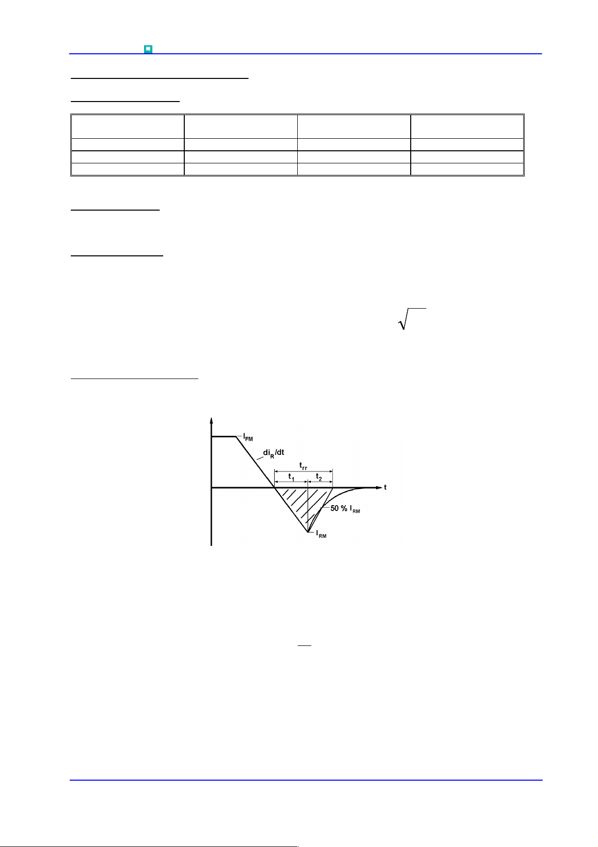
4.0 Reverse recovery ratings
(i) Qra is based on 50% Irm chord as shown in Fig.(a) below.
RRM
(V)
V
RSM
(V)
IDICIBAV ⋅+⋅+⋅+= )ln(
FFFF
V
dc
R
(V)
(ii) Qrr is based on a 150µs integration time.
s
µ
150
I.e.
(iii)
Data Sheet. Types M2408N#020 to M2408N#060 Issue 2 Page 3 of 11 July, 2004
=
FactorK =
dtiQ
.
rrrr
∫
0
t
1
t
2

WESTCODE
f
WESTCODE An IXYS Company Fast Recovery Diode Types M2408N#020 to M2408N#060
WESTCODEWESTCODE
5.0 Reverse Recovery Loss
The following procedure is recommended for use where it is necessary to include reverse recovery loss.
From waveforms of recovery current obtained from a high frequency shunt (see Note 1) and reverse
voltage present during recovery, an instantaneous reverse recovery loss waveform must be constructed.
Let the area under this waveform be E joules per pulse. A new sink temperature can then be evaluated
from:
)(
Where k = 0.2314 (°C/W)/s
E
= Area under reverse loss waveform per pulse in joules (W.s.)
= Rated frequency in Hz at the original sink temperature.
R
= d.c. thermal resistance (°C/W)
thJK
The total dissipation is now given by:
originaltot
NOTE 1 - Reverse Recovery Loss by Measurement
This device has a low reverse recovered charge and peak reverse recovery current. When measuring the
charge, care must be taken to ensure that:
(a) AC coupled devices such as current transformers are not affected by prior passage of high
amplitude forward current.
(b) A suitable, polarised, clipping circuit must be connected to the input of the measuring oscilloscope
to avoid overloading the internal amplifiers by the relatively high amplitude forward current signal.
(c) Measurement of reverse recovery waveform should be carried out with an appropriate critically
damped snubber, connected across diode anode to cathode. The formula used for the calculation of this
snubber is shown below:
)()(
[]
fEWW
⋅+=
RfkETT ⋅+⋅−=
thJKMAXJSINK
2
R
Where: Vr= Commutating source voltage
6.0 Snubber Components When selecting snubber components, care m ust be taken not to us e excessively large values of snubber
capacitor or excessively sm all values of snubber re sistor. Such exc essive com ponent values may lead to
device damage due to the large resultant values of snubber dis charge current. If required, please cons ult
the factory for assistance.
Data Sheet. Types M2408N#020 to M2408N#060 Issue 2 Page 4 of 11 July, 2004
V
⋅= 4
C
R = Snubber resistance
r
di
C
⋅
dt
S
= Snubber capacitance
S

WESTCODE
WESTCODE An IXYS Company Fast Recovery Diode Types M2408N#020 to M2408N#060
WESTCODEWESTCODE
7.0 Computer Modelling Parameters
7.1 Device Dissipation Calculations
4
2
00
2
I
=
AV
Where VT0 = 1.065V, rT = 0.122mΩ
2
rff
⋅⋅
T
WrffVV
⋅⋅⋅++−
AVTTT
ff = form factor (normally unity for fast diode applications)
∆
T
W
The forward characteristic I
(i) the well established V
((iiii))
=
AV
a set of constants A, B, C, and D forming the coefficients of the representative equation for V
R
th
TTT
−=∆
)(
7.2 Calculation of V
terms of I
given below:
F
KMAXj
using ABCD Coefficients
F
Vs VF, on page 6 is represented in two ways;
F
and rT tangent used for rating purposes and
T0
IDICIBAV ⋅+⋅+⋅+= )ln(
FFFF
in
F
The constants, derived by curve fitting software, are given in this report for both hot and cold
characteristics. The resulting values for V
which is limited to that plotted.
A
B
C
D
8.0 Frequency Ratings The curves illustrated in figures 8 to 16 are for guidance only and are superseded by the maxim um ratings
shown on page 1.
9.0 Square wave ratings These ratings are given for load component rate of rise of forward current of 100 and 500 A/µs.
10.0 Duty cycle lines The 100% duty cycle is represented on all the ratings by a straight line. Other duties c an be included as
parallel to the first.
agree with the true device characteristic over a current range,
F
25°C Coefficients 150°C Coefficients
0.4179024 0.103541587
0.09763557 0.098139
5.3723×10
3.45472×10
-5
-3
3.95463×10
8.071285×10
-5
-3
Data Sheet. Types M2408N#020 to M2408N#060 Issue 2 Page 5 of 11 July, 2004

WESTCODE
WESTCODE An IXYS Company Fast Recovery Diode Types M2408N#020 to M2408N#060
WESTCODEWESTCODE
Curves
Figure 1 – Forward characteristics of Limit device Figure 2 – Maximum forward recovery voltage
100
(V)
FRM
M2408N#020-060
Issue 2
150°C
(A)
FM
10000
M2408N#020-060
Issue 2
150°C 25°C
1000
Instantaneous forward current - I
100
00.511.522.5
Maximum instantaneous forward voltage - V
Figure 3 - Recovered charge, Q
1000
M2408N#020-060
Issue 2
Tj = 150°C
10
Maximum forward recovery voltage - V
1
(V)
FM
rr
2000A
1500A
1000A
500A
Figure 4 - Recovered charge, Qra (50% chord)
100 1000 10000
Rate of rise of forward current - di/dt (A/µs)
1000
M2408N#020-060
Issue 2
Tj = 150°C
25°C
2000A
1500A
1000A
500A
(µC)
rr
100
Total recovered charge - Q
10
1 10 100 1000
Data Sheet. Types M2408N#020 to M2408N#060 Issue 2 Page 6 of 11 July, 2004
Commutation rate - di/dt (A/µs)
100
(µC)
ra
Recovered charge - Q
10
1
1 10 100 1000
Commutation rate - di/dt (A/µs)

WESTCODE
WESTCODE An IXYS Company Fast Recovery Diode Types M2408N#020 to M2408N#060
WESTCODEWESTCODE
Figure 5 - Maximum reverse current, I
1000
M2408N#020-060
Issue 2
Tj = 150°C
100
(A)
rm
10
Reverse recovery current - I
1
1 10 100 1000
Commutation rate - di/dt (A/µs)
rm
2000A
1500A
1000A
500A
Figure 6 - Maximum recovery time, trr (50% chord)
10
M2408N#020-060
Issue 2
Tj = 150°C
(µs)
rr
Recovery time - t
1
1 10 100 1000
Commutation rate - di/dt (A/µs)
2000A
1500A
1000A
500A
Figure 7 – Reverse recovery energy per pulse Figure 8 - Sine wave energy per pulse
1000
M2408N#020-060
Issue 2
Tj = 150°C
=300V
V
r
(mJ)
r
100
Energy per pulse - E
10
1 10 100 1000
Commmutation rate - di/dt (A/µs)
2000A
1500A
1000A
500A
500A
1.00E+03
1.00E+02
1.00E+01
Energy per pulse (J)
1.00E+00
1.00E-01
M2408N#020-060
Issue 2
Tj = 150°C
6000A
4000A
3000A
2000A
1000A
1.00E-05 1.00E-04 1.00E-03 1.00E-02
Pulse width (s)
Data Sheet. Types M2408N#020 to M2408N#060 Issue 2 Page 7 of 11 July, 2004

WESTCODE
WESTCODE An IXYS Company Fast Recovery Diode Types M2408N#020 to M2408N#060
WESTCODEWESTCODE
Figure 9 - Sine wave frequency vs. pulse width Figure 10 - Sine wave frequency vs. pulse width
1.00E+05
1.00E+04
1.00E+03
Frequency (Hz)
1000A
2000A
3000A
4000A
6000A
M2408N#020-060
100% Duty Cycle
Issue 2
TK = 55°C
1.00E+05
1.00E+04
1.00E+03
Frequency (Hz)
1000A
2000A
3000A
4000A
6000A
M2408N#020-060
100% Duty Cycle
Issue 2
TK = 85°C
1.00E+02
1.00E+01
1.00E-05 1.00E-04 1.00E-03 1.00E-02
Pulse width (s)
1.00E+02
1.00E+01
1.00E-05 1.00E-04 1.00E-03 1.00E-02
Pulse width (s)
Figure 11 - Square wave energy per pulse Figure 12 - Square wave energy per pulse
1.00E+03
1.00E+02
1.00E+01
M2408N#020-060
Issue 2
di/dt =100A/µs
Tj = 150°C
1.00E+03
1.00E+02
1.00E+01
M2408N#020-060
Issue 2
di/dt =500A/µs
Tj = 150°C
6000A
4000A
3000A
2000A
1000A
2000A
1000A
4000A
3000A
6000A
Pulse width (s)
Energy per pulse (J)
1.00E+00
1.00E-01
1.00E-05 1.00E-04 1.00E-03 1.00E-02
Pulse width (s)
Energy per pulse (J)
1.00E+00
1.00E-01
1.00E-05 1.00E-04 1.00E-03 1.00E-02
Data Sheet. Types M2408N#020 to M2408N#060 Issue 2 Page 8 of 11 July, 2004

WESTCODE
WESTCODE An IXYS Company Fast Recovery Diode Types M2408N#020 to M2408N#060
WESTCODEWESTCODE
Figure 13 - Square wave frequency vs. pulse width Figure 14 - Square wave frequency vs. pulse width
1.00E+05
1.00E+04
1000A
2000A
M2408N#020-060
Issue 2
di/dt =100A/µs
100% Duty Cycle
TK=55°C
1.00E+05
1.00E+04
1000A
2000A
M2408N#020-060
di/dt =500A/µs
100% Duty Cycle
Issue 2
TK = 55°C
3000A
4000A
1.00E+03
Frequency (Hz)
1.00E+02
1.00E+01
1.00E-05 1.00E-04 1.00E-03 1.00E-02
6000A
Pulse width (s)
1.00E+03
Frequency (Hz)
1.00E+02
1.00E+01
3000A
4000A
6000A
1.00E-05 1.00E-04 1.00E-03 1.00E-02
Pulse width (s)
Figure 15 - Square wave frequency vs. pulse width Figure 16 - Square wave frequency vs. pulse width
1.00E+05
1.00E+04
1.00E+03
Frequency (Hz)
1000A
2000A
3000A
4000A
6000A
M2408N#020-060
Issue 2
di/dt =100A/µs
TK = 85°C
100% Duty Cycle
1.00E+05
1.00E+04
1.00E+03
Frequency (Hz)
1000A
2000A
3000A
4000A
M2408N#020-060
Issue 2
di/dt =500A/µs
TK = 85°C
100% Duty Cycle
6000A
1.00E+02
1.00E+01
1.00E-05 1.00E-04 1.00E-03 1.00E-02
Data Sheet. Types M2408N#020 to M2408N#060 Issue 2 Page 9 of 11 July, 2004
Pulse width (s)
1.00E+02
1.00E+01
1.00E-05 1.00E-04 1.00E-03 1.00E-02
Pulse width (s)

WESTCODE
WESTCODE An IXYS Company Fast Recovery Diode Types M2408N#020 to M2408N#060
WESTCODEWESTCODE
Figure 17 – Maximum surge and I2t ratings
100000
(A)
FSM
10000
Total peak half sine surge current - I
1000
I2t: V
I2t: VR=60% V
I
FSM
I
FSM
Tj (initial) = 150°C
10V
≤
RRM
: V
RRM
: VR=60% V
M2408N#020-060
Issue 2
1 35101 510 50100
Duration of surge (ms) Duration of surge (cycles @ 50Hz)
≤10V
RRM
RRM
1.00E+08
1.00E+07
1.00E+06
2
2
s)
t (A
Maximum I
Figure 18 – Transient thermal impedance
0.1
M2408N#020-060
Issue 2
0.01
0.001
Thermal impedance (K/W)
0.0001
0.0001 0.001 0.01 0.1 1 10 100
SSC 0.044K/W
DSC 0.022K/W
Time (s)
Data Sheet. Types M2408N#020 to M2408N#060 Issue 2 Page 10 of 11 July, 2004

WESTCODE
WESTCODE An IXYS Company Fast Recovery Diode Types M2408N#020 to M2408N#060
WESTCODEWESTCODE
Outline Drawing & Ordering Information
100A325
Housing option NC and NT
ORDERING INFORMATION (Please quote 10 digit code as bel ow)
M2408 N#
Fixed
Type Code
Order code: M2408ND040 – 400V V
IXYS Semiconductor GmbH
Edisonstraße 15
D-68623 Lampertheim
Tel: +49 6206 503-0
Fax: +49 6206 503-627
E-mail: marcom@ixys.de
IXYS Corporation
3540 Bassett Street
Santa Clara CA 95054 USA
Tel: +1 (408) 982 0700
Fax: +1 (408) 496 0670
E-mail: sales@ixys.net
The information contained herein is confidential and is protected by Copyright. The information may not be used or disclosed except
with the written permission of and in the manner permitted by the proprietors Westcode Semiconductors Ltd.
In the interest of product improvement, Westcode reserves 7he right to change specifications at any time without prior notice.
Devices with a suffix code (2-letter,3-letter or letter/digit/letter combination) added to their generic code are not necessarily subject to
the conditions and limits contained in this report.
NC = 27.7mm Clamp hei ght capsule, ND = 21mm Cl amp height capsule,
NT = 27.7mm Clamp hei ght rupture rated capsule
, 21mm clamp height capsule.
RRM
WESTCODE
An IXYS Company
www.westcode.com
www.ixys.com
Housing option ND
Voltage code
/100
V
RRM
02-06
Westcode Semiconductors Ltd
Langley Park Way, Langl ey Park,
Chippenham, Wi l tshire SN15 1GE.
E-mail: WSL.sales@westcode.com
Westcode Semiconductors Inc
Long Beach CA 90807 USA
E-mail: WSI.sales@westcode.com
0
Fixed code
Tel: +44 (0)1249 444524
Fax: +44 (0)1249 659448
3270 Cherry Avenue
Tel: +1 (562) 595 6971
Fax: +1 (562) 595 8182
© Westcode Semiconductors Ltd.
Data Sheet. Types M2408N#020 to M2408N#060 Issue 2 Page 11 of 11 July, 2004

WESTCODE
WESTCODE An IXYS Company Fast Recovery Diode Types M2408N#020 to M2408N#060
WESTCODEWESTCODE
Data Sheet. Types M2408N#020 to M2408N#060 Issue 2 Page 12 of 11 July, 2004
 Loading...