

Westcode Semiconductors M1583VC400, M1583VC450 Data Sheet

Date:- 2 Nov, 2001
WESTCODE
Fast Recovery Diode
Types M1583VC400 to M1583VC450
Absolute Maximum Ratings
VOLTAGE RATINGS
V
RRM
V
RSM
I
F(AV)
I
F(AV)
I
F(AV)
I
F(RMS)
I
F(d.c.)
I
FSM
I
FSM2
I2tI
I2t
T
HS
T
stg
Repetitive peak reverse voltage, (note 1) 4000-4500 V
Non-repetitive peak reverse voltage, (note 1) 4100-4600 V
OTHER RATINGS
Mean forward current, T
Mean forward current. T
Mean forward current. T
Nominal RMS forward current, T
D.C. forward current, T
Peak non-repetitive surge tp=10ms, VRM=0.6V
Peak non-repetitive surge tp=10ms, V
2
t capacity for fusing tp=10ms, VRM=0.6V
2
t capacity for fusing tp=10ms, V
I
Operating temperature range -40 to +150 °C
Storage temperature range -40 to +150 °C
(note 6)
=55°C, (note 2) 1583 A
sink
=100°C, (note 2) 1030 A
sink
=100°C, (note 3) 624 A
sink
=25°C, (note 2) 2963 A
sink
=25°C, (note 4) 2569 A
sink
, (note 5) 24.8 kA
RRM
≤
10V, (note 5)
RM
, (note 5) 3.08×10
RRM
≤
10V, (note 5)
RM
Data Sheet Issue:- 1
MAXIMUM
LIMITS
MAXIMUM
LIMITS
27.3 kA
6
3.73×10
6
UNITS
UNITS
A2s
A2s
Notes:-
1)
De-rating factor of 0.13% per °C is applicable for Tj below 25°C.
2)
Double side cooled, single phase; 50Hz, 180° half-sinewave.
3)
Single side cooled, single phase; 50Hz, 180° half-sinewave.
4)
Double side cooled.
5)
Half-sinewave, 150°C Tj initial.
Data Sheet. Types M1583VC400 to M1583VC450 Issue 1 Page 1 of 11 November, 2001

WESTCODE
Positive development in power electronics
Characteristics
M1583VC400 to M1583VC450
PARAMETER MIN. TYP. MAX. TEST CONDITIONS
V
V
r
S
Maximum peak forward voltage - - 2.8 IFM=2000A V
FM
Threshold voltage - - 1.693 V
0
Slope resistance - - 0.525
(Note 1)
UNITS
m
- - 110 di/dt = 1000A/µs
V
I
Q
Q
I
t
R
RRM
rm
rr
Maximum forward recovery voltage
FRM
Peak reverse current - - 150 Rated V
Reverse Recovery Charge - 2000 - µC
rr
Recovered charge, 50% Chord - 1100 1500 µC
ra
Reverse Recovery Current - 500 - A
- - 70 di/dt = 1000A/µs, Tj=25°C
RRM
I
=1000A, tp=500µs, di/dt=200A/µs,
FM
=50V, 50% Chord.
V
r
Reverse recovery time, 50% Chord - 5.0 -
- - 0.016 Double side cooled
Thermal resistance, junction to heatsink
th(j-hs)
- - 0.032 Single side cooled
V
mA
µs
K/W
F Mounting force 27 - 34 kN
W
Weight - 1000 - g
t
Notes:-
1) Unless otherwise indicated T
=150°C.
j
Ω
Introduction
The M1583VC400-450 fast recovery diode range has controlled reverse recovery characteristics.
Devices with a suffix code (2 letter or letter/digit/letter combination) added to their generic code are not
necessarily subject to the conditions and limits contained in this report.
Data Sheet. Types M1583VC400 to M1583VC450 Issue 1 Page 2 of 11 November, 2001
WESTCODE
Notes on Ratings and Characteristics
1.0 Voltage Grade Table
Positive development in power electronics
M1583VC400 to M1583VC450
Voltage Grade V
40 4000 4100 2000
42 4200 4300 2040
44 4400 4500 2080
45 4500 4600 2100
2.0 De-rating Factor A blocking voltage de-rating factor of 0.13% per °C is applicable to this device for Tj below 25°C.
3.0 ABCD Constants These constants (applicable only over current range of VF characteristic in Figure 1) are the coefficients of
the expression for the forward characteristic given below:
RRM
(V)
)ln(
where IF = instantaneous forward current.
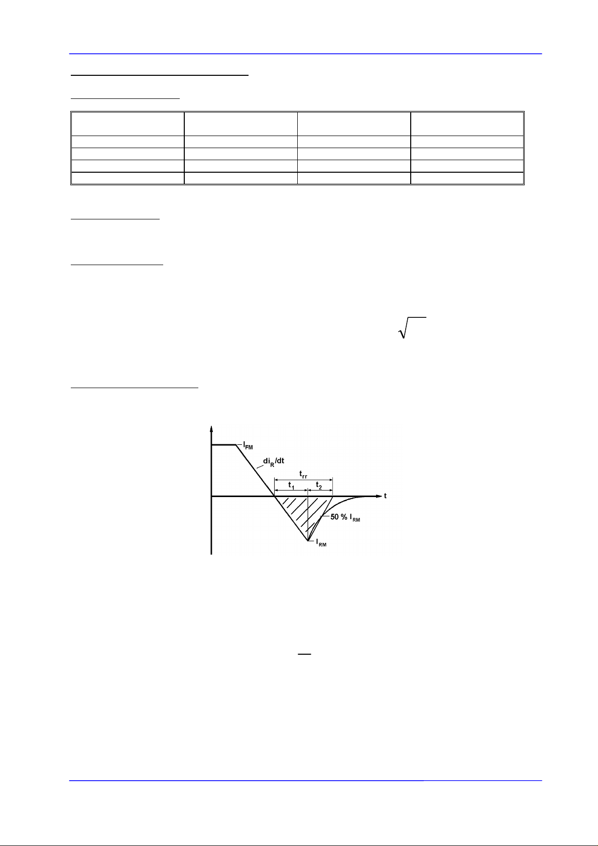
4.0 Reverse recovery ratings (i) Qra is based on 50% Irm chord as shown in Fig.(a) below.
V
RSM
(V)
IDICIBAV
⋅+⋅+⋅+=
FFFF
V
dc
R
(V)
(ii) Qrr is based on a 150µs integration time.
s
µ
150
I.e.
(iii)
Data Sheet. Types M1583VC400 to M1583VC450 Issue 1 Page 3 of 11 November, 2001
=
FactorK
dtiQ
.
rrrr
∫
0
t
1
=
t
2

WESTCODE
)
5.0 Reverse Recovery Loss
The following procedure is recommended for use where it is necessary to include reverse recovery loss.
From waveforms of recovery current obtained from a high frequency shunt (see Note 1) and reverse
voltage present during recovery, an instantaneous reverse recovery loss waveform must be constructed.
Let the area under this waveform be E joules per pulse. A new sink temperature can then be evaluated
from:
Positive development in power electronics
M1583VC400 to M1583VC450
[]
Where k = 0.2314 (°C/W)/s
E
= Area under reverse loss waveform per pulse in joules (W.s.)
f
= Rated frequency in Hz at the original sink temperature.
R
The total dissipation is now given by:
This device has a low reverse recovered charge and peak reverse recovery current. When measuring the
charge, care must be taken to ensure that:
amplitude forward current.
to avoid overloading the internal amplifiers by the relatively high amplitude forward current signal.
= d.c. thermal resistance (°C/W)
th(J-Hs
fEWW
originaltot
NOTE 1 - Reverse Recovery Loss by Measurement
(a) AC coupled devices such as current transformers are not affected by prior passage of high
(b) A suitable, polarised, clipping circuit must be connected to the input of the measuring oscilloscope
)()(
⋅+=
⋅+⋅−=
RfkETT
−
HsJthMAXJSINK
)()(
(c) Measurement of reverse recovery waveform should be carried out with an appropriate critically
damped snubber, connected across diode anode to cathode. The formula used for the calculation of this
snubber is shown below:
2
R
Where: Vr= Commutating source voltage
4
V
⋅=
C
R = Snubber resistance
r
di
C
⋅
dt
S
= Snubber capacitance
S
Data Sheet. Types M1583VC400 to M1583VC450 Issue 1 Page 4 of 11 November, 2001
 Loading...