

Soft Recovery Diode
Types
The data sheet
on
M1565V#400 to M1565V#450
the subsequent pages of this document is a scanned copy of existing
data for this product.
(Rating Report 97007 Issue
1)
This data reflects the old part number for this product which is: SM36-45C/FXC394.
This part number must
NOT be used for ordering purposes - please use the ordering
particulars detailed below.
limitations of this data are as follows:
The
Device
VF outline drawing 0N43)
Only
no
longer available for grades 36 & 38 (3600V & 3800V
in
datasheet
VRRMNoRM)
The following links will direct you to the appropriate outline drawings
Outline
W6
- 33mm clamp height capsule
Outline W43 - 26mm clamp height capsule
Where any information
the product matrix page differs from that
in
the following data,
on
the product matrix must be considered correct
An electronic data sheet for this product
For further information
on
this product, please contact your local ASM or distributor.
is
presently
in
preparation.
Alternatively,
please contact Westcode as detailed below.
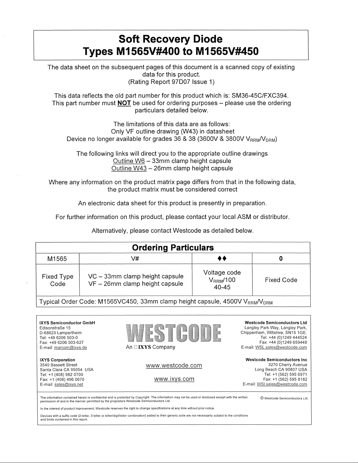
Ordering Particulars
M1565
Fixed Type
Code
VC - 33mm clamp height capsule
VF - 26mm clamp height capsule
Typical Order Code: M1565VC450, 33mm clamp height capsule, 4500V
IXYS
Semiconductor
EdisonstralSe 15
0-68623 Lampertheim
Tel:
+496206
Fax:
+496206
E-mail:
marcom@ixys.de
IXYS
Corporation
3540 Bassett Street
Santa
Clara CA 95054 USA
Tel:
+1
(408) 982 0700
Fax:
+1
(408) 496 0670
E-mail:
sales@ixys.net
The
information contained herein is confidential and is protected by Copyright. The information may not
of
permission
In the interest
Devices with a suffix code (2-1etter, 3-1eller or letter/digitlletter combination) added
and limits contained in this
and in the manner permitted by the proprietors Westcode Semiconductors Ltd.
of
product improvement, Westcode reserves the right to change specifications at any time without prior notice
GmbH
503-0
503-627
report
V#
An
LnXYS Company
www.westcode.com
www.ixys.com
••
Voltage code
V
/100 Fixed Code
RRM
40-45
be
used or disclosed except with the written
to
their generic code are not necessarily subject to the conditions
0
VRRMl'v'ORM
Westcode
Langley Park Way, Langley Park,
Chippenham, Wiltshire, SN15 1GE.
E-mail: WSL.sales@westcode.com
Westcode
E-mail: WSl.sales@westcodecom
Semiconductors
Tel: +44 (0)1249444524
Fax: +44
Long Beach CA
(0)1249 659448
Semiconductors
3270 Cherry Avenue
Tel:
Fax:
© Westcode Semiconductors Ltd
90807 USA
+1
(562) 595 6971
+1
(562) 595 8182
Ltd
Inc
ETOE@J
SEMICONDUCTORS
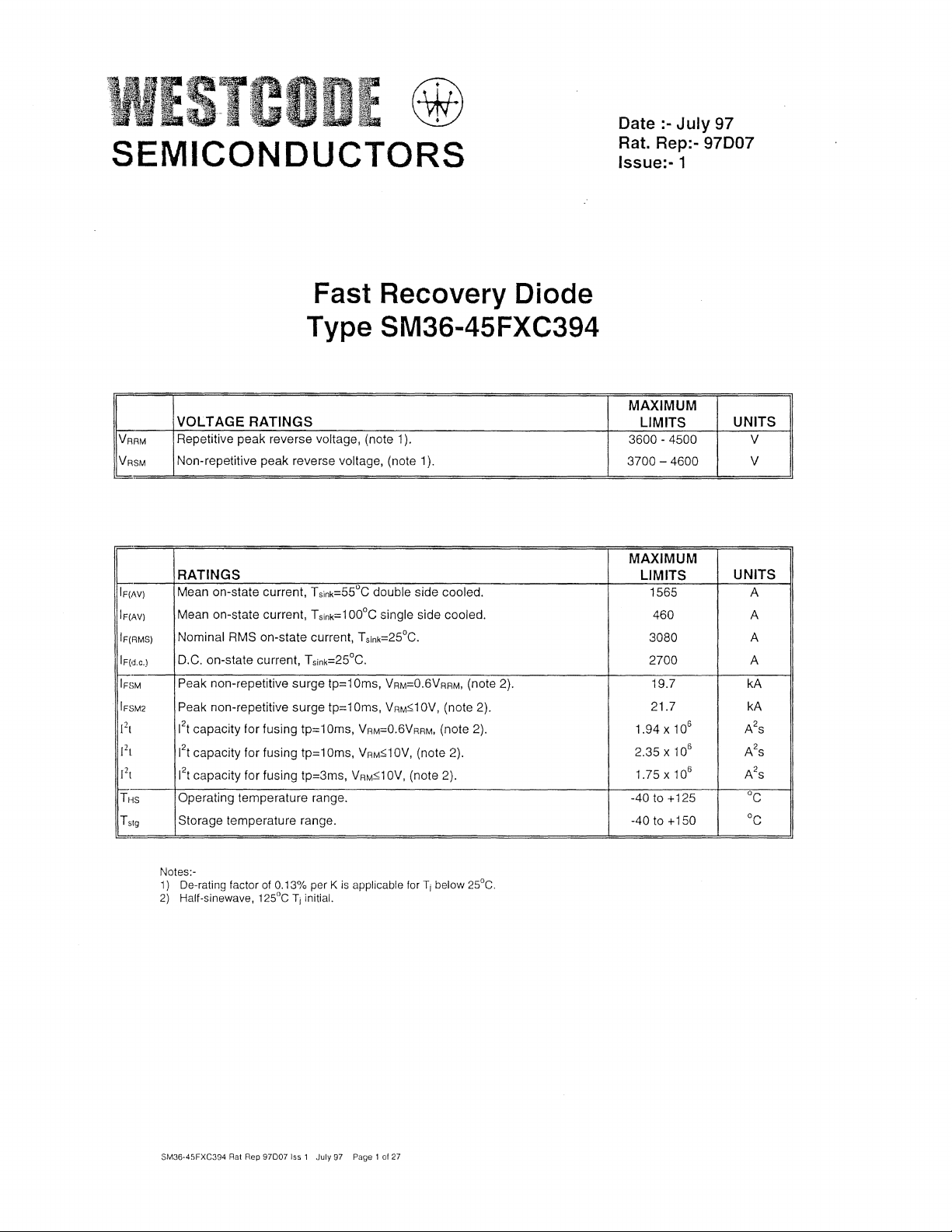
Fast Recovery Diode
Type SM36-45FXC394
VOLTAGE RATINGS
VAAM
VASM
IF(Av)
IF(Av)
IF(AMS)
IF(d.c.)
f:-.
IFsM
IFSM2
121
121
2
I
t
TliS
T
stg
Repetitive
Non-repetitive
RATINGS
Mean on-state current, T
Mean on-state current,
Nominal
D.C. on-state current, Tsink=25°C.
Peak
Peak non-repetitive
2
1
t capacity
2
t
1
ft
Operating
Storage
peak
reverse voltage, (note 1).
peak
reverse voltage, (note 1).
sink=550C double side cooled.
Tsink= 1 OO°C
RMS on-state current, Tslnk=25°C.
non-repetitive
for
capacity
capacity
for
for
temperature
temperature
surge
tp=10ms,
surge
tp=1 Oms,
fusing tp=1
fusing tp=1
fusing tp=3ms,
Oms,
Oms,
range.
range.
single side cooled.
VAM=0.6VAAM,
VAM~1
VAM=0.6VAAM,
VAM~1
OV,
(note 2).
VAM~1
OV,
(note 2).
OV,
(note 2).
(note 2).
(note 2).
Date :-July 97
Rat. Rep:-
97007
Issue:- 1
MAXIMUM
LIMITS
3600 -4500
3700
-4600
MAXIMUM
LIMITS
1565 A
460
3080
2700
19.7
21.7
to
to
x 10
x 10
+125
+150
6
6
6
1.94
2.35
1.75x10
-40
-40
UNITS
V
V
UNITS
A
A
A
kA
kA
A2s
A2s
A2s
°c
°c
Notes:-
1)
De-rating factor of 0.13% per K
2)
Half-sinewave,
SM36·45FXC394
Aat
Rep
12SoC
97007
Tj
initial.
Iss 1 July
is
applicable
97
Page 1
for
Tj
below
2SoC.
01
27
CHARACTERISTICS
Maximum peak on-state voltage.
VFM
Threshold voltage. -
Vo
Slope resistance.
rs
Peak reverse current. -
IRRM
Thermal resistance.
Re
Max. forward Recovery voltage
VFR
Reverse recovered charge
ORA
F
Mounting torque.
Weight.
Wt
Notes:-
1)
Unless otherwise indicated
3) Single
side
cooled
MIN
-
-
-
-
27
-
,/"
TJ~125°C.
TYP MAX TEST CONDITIONS
1.8 IFM=2000A.
1.09
-
0.36
100
-
-
-
-
-
-
kS'
I.
6r
t't~~,,/
iq·~2--q$
.
2)
4)
Rated V
10
Rated V
0.018
Junction
0.036
Junction to heatsink, Note 3
90
diF/dt=1000AlJ.(s
2000
IFM=1
34
.
RRM
RRM
25°C.
to
heatsink, Note 2
OOOA,
diR/dt=200Al~lS
-
Double
side
tp~500Jls,VR~50V
cooled.
note 4
UNITS
V
V
mQ
mA
mA
KJW
KJW
V
~lC
kN
kg
ORDERING INFORMATION
SM
Fixed Voltage Codes Fixed Fixed
Type Code
Typical order
SM36-45FXC394 Rrlt
code:
SM38FXC394 :-3800V
RAp
97007
Iss,
July 97 Page 2
• •
36
- 45
VqRM
26.5mm clamp heiqht capsule.
01
2.7
FXC
Outline Code
(Please quote 10 diqit code as below)
394
Type Code
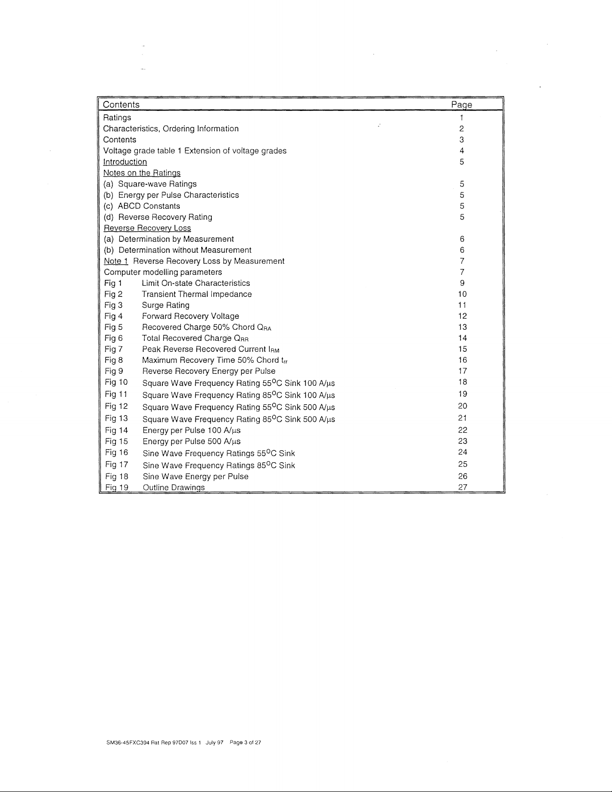
Contents
Page
Ratings 1
Characteristics, Ordering Information 2
Contents 3
Voltage grade table 1 Extension of voltage grades 4
Introduction 5
Notes
on
the Ratings
Square-wave Ratings
(a)
(b)
Energy per Pulse Characteristics
(c)
ABeD
Constants 5
(d)
Reverse Recovery Rating 5
Reverse Recovery Loss
(a) Determination by Measurement 6
(b) Determination without Measurement 6
Note 1 Reverse Recovery Loss by Measurement
Computer modelling parameters 7
Fig 1 Limit On-state Characteristics
Fig 2 Transient Thermal Impedance
Fig 3 Surge Rating
Fig 4
Fig S Recovered Charge
Fig 6 Total Recovered Charge
Fig 7 Peak Reverse Recovered Current
Fig 8 Maximum Recovery Time
Fig 9 Reverse Recovery Energy per
Fig 10
Fig
Fig 12
Fig 13
Fig 14 Energy per Pulse 100
Fig
Fig
Fig 17
Forward Recovery Voltage
Square
Wave Frequency Rating S50C Sink 100 A/',lS
11
Square Wave Frequency Rating
Square Wave Frequency Rating
Square Wave Frequency Rating
lS
Energy per Pulse 500
16
Sine Wave Frequency Ratings
Sine Wave Frequency Ratings
SO%
Ai',lS
Ai',lS
Chord
QRA
QRR
50% Chord
Pulse
5SoC
85°C
IRM
trr
85°C
5SoC
85°C
Sink
Sink
Sink 100 A/',lS
Sink
SOO
A/',lS
Sink
SOO
A/',lS
Fig 18 Sine Wave Energy per Pulse
Fiq 19 Outline Drawinqs
5
5
7
9
10
11
12
13
14
15
16
17
18
19
20
21
22
23
24
25
26
27
SM36-4SFXC394
Rat
Rep 97D07
Iss
1 July 97 Page 3
at
27
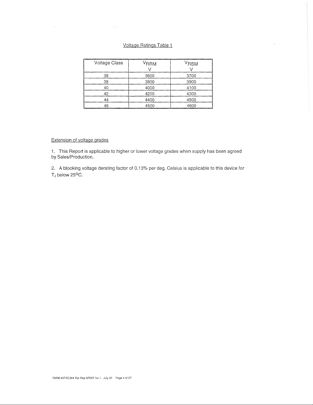
Voltage Ratings Table 1
Voltage Class
VRRM
VRSM
V V
36
3600
38 3800
3700
3900
40 4000 4100
42 4200 4300
44 4400 4500
45
4500 4600
Extension of voltage grades
1.
This Report is applicable to higher
Sales/Production.
by
or
lower voltage grades when supply has been agreed
2. A blocking voltage derating factor of 0.13% per deg. Celsius is applicable to this device for
TJ
below
2SoC.
SM36-45FXC394 Ral Rep
97007
Iss 1 July 97 Page 4
of
27
INTRODUCTION
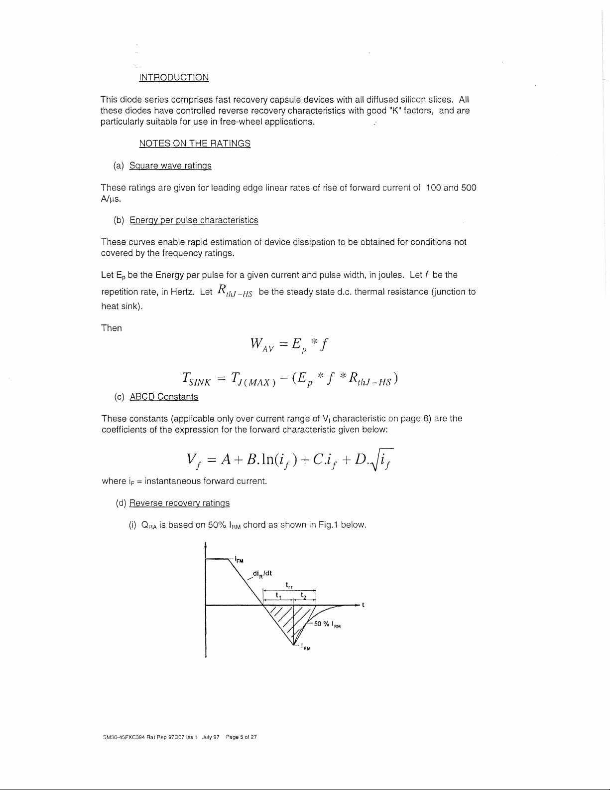
This diode series comprises fast recovery capsule devices with all diffused silicon slices.
these diodes have controlled reverse recovery characteristics with good
particularly suitable for use
NOTES
(a)
Square wave ratings
These ratings are given for leading edge linear rates of rise
N'}ls.
(b)
Energy per pulse characteristics
These curves enable rapid estimation of device dissipation to
covered
Let
repetition rate,
heat sink).
Then
by
Ep
be
the Energy per pulse for a given current and pulse width,
ON
the frequency ratings.
in
Hertz. Let
in
free-wheel applications.
THE RATINGS
R'hJ
-HS
of
forward current of 1 00 and 500
be
be
the steady state d.c. thermal resistance (junction to
"K"
factors, and are
obtained for conditions not
in
joules. Let f be the
TSINK
(c)
ABCD Constants
All
These constants (applicable only over current range
coefficients of the expression for the forward characteristic given below:
VI = A + B.lnCi
where
iF
= instantaneous forward current.
(d)
Reverse recovery ratings
(i)
ORA
is
based
on
50%
IRM
chord
as
shown
of
+ C.if +
)
f
in
VI
characteristic
Fig.1
below.
D.ji;
on
page
8)
are the
SM36-45FXC394
Rat
Rep 97D07 Iss 1 July 97 Page 5 of 27
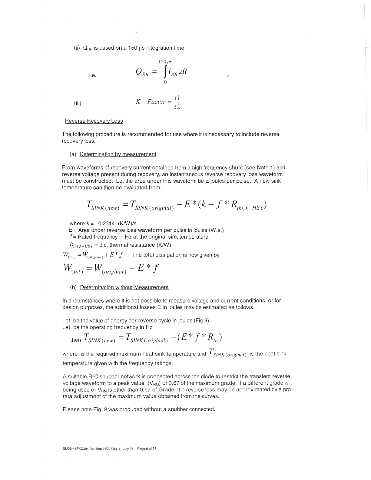
(ii)
ORR
is
based on a 150
i.e.
I-ls
integration time
K
(iii)
Reverse Recoverv Loss
The following procedure
recovery loss.
(a) Determination
From waveforms of recovery current obtained from a
reverse
must be constructed. Let the area under this waveform
temperature can then be evaluated from:
voltage present during recovery, an instantaneous reverse recovery loss waveform
is
by
measurement
-Factor
recommended for use where
TS1NK(new) = TS1NK(original)
where k = 0.2314 (K/W)/s
E = Area
f = Rated frequency
R
Vl'<11I1) =
W(IDl) = W(Original)
(J-HS)
tl1
under
reverse loss waveform per pulse
in
Hz at the original sink temperature.
= d.c. thermal resistance (K/W)
W(oriRilllll)
+ E * f The total dissipation
+ E * f
=-
tI
t2
-
E*
is
in
now given by
it
is necessary to include reverse
high
frequency shunt (see Note
be
E joules per pulse. A new sink
(k + f *
joules (W.s.)
Rth(J-HS»)
1)
and
(b) Determination without Measurement
In
circumstances where it
design purposes, the additional losses E in joules may
Let be the value of energy per reverse cycle
Let be the operating frequency in Hz
T
then SINK(llew) - SINK(origillal) -
where
temperature given with the frequency ratings.
A suitable R-C snubber network
voltage waveform to a peak value (V
being used
rata adjustment of the maximum value obtained from the curves.
Please note Fig. 9 was produced without a snubber connected.
SM36-45FXC394 Ral Rep 97007 Iss I July 97 Page 6
is
the required maximum heat sink temperature
or
V
RM
is
not possible to measure voltage and current conditions, or for
be
estimated as follows.
in
joules (Fig 9).
-T
is
connected across the diode to restrict the transient reverse
) of 0.67
RM
is
other than 0.67 of Grade, the reverse loss may be approximated by a pro
01
27
(E*f*
of
the maximum grade. If a different grade
R )
th
and
TS1NK(original)
is
the heat sink
is
NOTE 1
Reverse Recoverv Loss by Measurement
This device has a
measuring the charge care must be taken to ensure that:
(a) a.c. coupled devices such as current transformers are not affected by prior passage of
high amplitude forward current.
(b) A suitable, polarised, clipping circuit must be connected to the input of the measuring
oscilloscope to avoid overloading the internal amplifiers by the relatively high amplitude
forward current
(c) Measurement of reverse recovery waveform should be carried out with an appropriate
critically damped snubber, connected across diode anode to cathode.
Please note Fig. 9 was produced without a snubber connected.
Where V
Computer
==
R
C
==
==
R
Modelling Parameters
low reverse recovered charge and peak reverse recovery current.
signal.
R2
=
Commutating source voltage
Snubber capacitance
Snubber resistance
4*
R
V
C * di /
elt
When
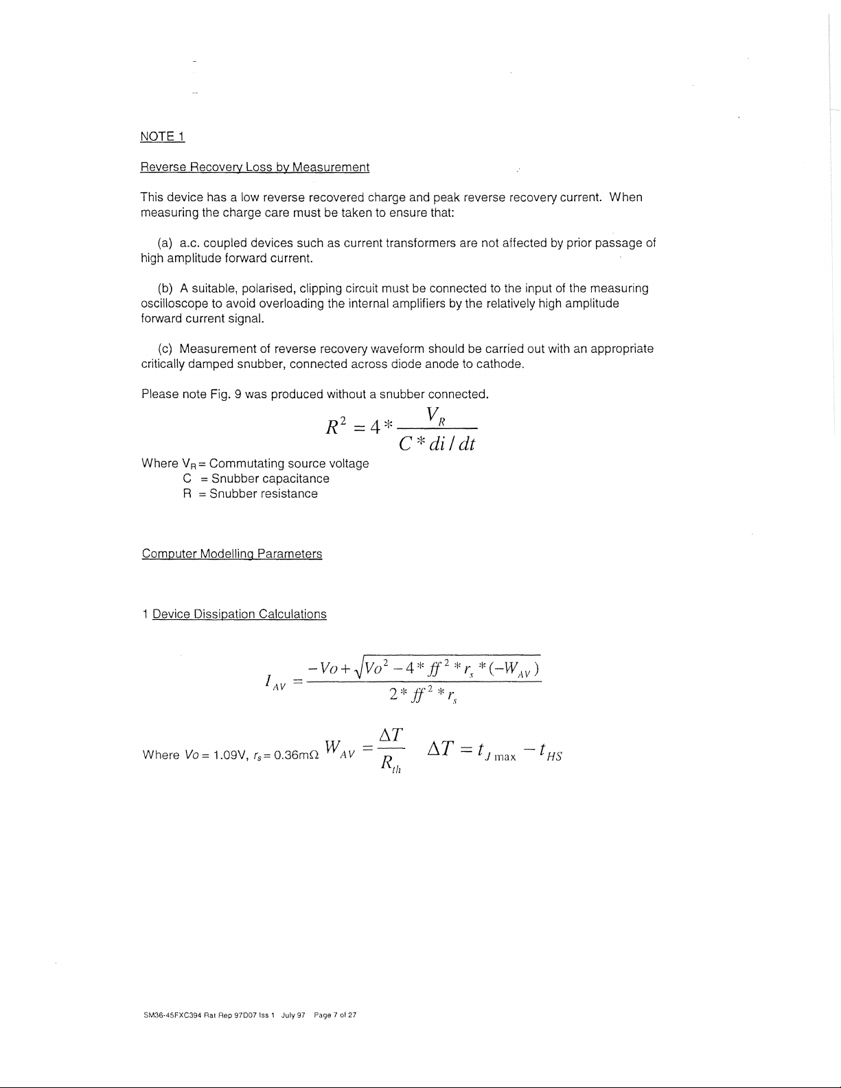
1 Device Dissipation Calculations
-Vo+~Vo2-4*jj'2*r
II
V
O,36mQ W
Where
Vo
==
1.09V,
rs
T
•
==
*(-w )
s ,IV
'j"
jlj'
2
'j"
....
"'
2
r
s
!1T
!J.T
A
V
= t
Jmax
- t
HS
S~A36·45FXC394
Rat Rep
97007
Iss'
July
97
Page 7 of 27
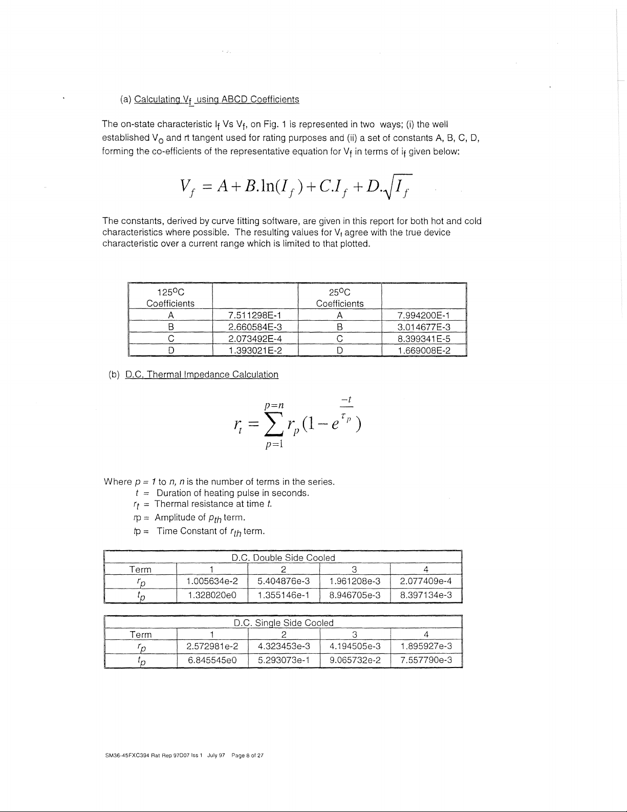
(a)
Calculating
The on-state characteristic
established Va and
forming the co-efficients of the representative equation for
Vf
using ABCD Coefficients
If
Vs
Vf,
on
Fig. 1
is
rt
tangent used for rating purposes
V
= A + B.ln(J
f
f)
represented
and
+
C.I
in
two ways;
(ii) a set
Vf
in
terms of if given below:
+ D .
f
(i)
of
constants
.[i;
the well
A,
B,
C,
D,
The constants, derived by curve fitting software, are given
characteristics where possible. The resulting values for
characteristic over a current range which
1250C
Coefficients
A 7.511298E-1
B 2.660584E-3 B
C 2.073492E-4
0 1.393021 E-2
(b)
D.C. Thermal Impedance Calculation
r;
==
is
limited to that plotted.
Coefficients
jJ=n
L
rp
(1-
250C
e'l' )
p=l
Where p = 1 to
t = Duration of heating pulse
rt = Thermal resistance at time
rp
tp
n,
n
is
the number of terms
= Amplitude of
= Time Constant of rth term.
Pth
term.
in
in
seconds.
t.
the series.
in
this report for both hot and cold
VI
agree with the true device
A
C
D
7.994200E-1
3.014677E-3
8.399341 E-5
1.669008E-2
-t
Term
rp
tp
Term
'R
tp
SM36·45FXC394
Rat Rep
D.C. Double Side Cooled
1 2
1.005634e-2
1.328020eO 1 .355146e-1
1 2 3
2.572981 e-2 4.323453e-3 4.194505e-3
6.845545eO 5.2930738-1 9.065732e-2
97007
Iss 1 July 97 Page B
5.404876e-3
D.C. Sinqle Side Cooled
01
27
1.961208e-3
8.946705e-3
3
I
I
I
L
4
2.077 40ge-4
8.397134e-3
4
1.895927e-3
7.557790e-3
!

Fig. 1 Forward
Characteristic
of
Limit
Device
10000
---.
CJ)
Q)
....
Q)
0-
E
«
----
......
c
Q)
....
....
:::l
o
"'0
~
S:
....
o
LL
CJ)
:::l
o
Q)
c
cO
.......
C
cO
......
CJ)
C
1000
i
!
:
I
I
I
I
;
!
I
I
i
i
!
i
I
I
I
I
25°C
I
I
I
I
I
I
V
/
/
V
/
V
V
V·-
j
v
IL
V
I
,/
/(
./
v
V
I
125°C
i-'"
V
/'
i
I
I
I
I
i
I
1
I
I
I
V
V
v
V
V
I
I
I
I
I
I
I
!
I
/
i
Vii
V
V
1/
/
~
I I
I
~
125°C
III
I
l
I
,
i
!
t
,
I
i
:
i
!
i
I
/'
h
II/.
;
V
fi
1/
VI
I
I
I
I
I
I I
i i I
I
I
,
I
I
,
I
//
I
I
A = 7.511298E-1
= 2.660584E-3
B
C = 2.073492E-4
o = 1.393021 E-2
-
A = 7.9942E-1
B = 3.014677E-3
C = 8.399341 E-5
o = 1.669008E-2
25°C
-
-
-
-
-
-
I
D":lno
I
I
I
•
,
,
If
I
I
I
I
I
I
I
I
I
I
I
I
j
I
,
I SM36-45CXC394
97007 Iss 1
0.8
I I
1.2
1.6
2
2.4 2.8
3.2
100
Maximum Instantaneous Forward Voltage (Volts)
a
I"'\f
07
,
3.6
4

0.1
1-----+---1--1----1-'-
Fig. 2 Transient Thermal Impedance (Junction
----+---+----f-+--j-+-f--H--------f
I
1
-1----1-
--~~~t:__-L~-"-
to
Heat Sink)
+-----.-+-----.,--.-.~
...
--~---~-.-->--.--.-
0.036
S.S.C
KIW
0.01
~
Q)
()
C
co
-0
Q)
r
0001
f-
I I I I I I I I I I I I I I I I I I
I .
~::tttW
I I jfW#t./=f=tttttw-=I-=t-=t=tltlU---=t----t-t-t=UtJI
..-
L
I I
~
t----r----t--+---f···-I--I+t-+-------j------~---·-->-->-
utttm
L
v
/
I
I--t----f-t--H+
I I I I I I I I I I I I I I I I I I I I I I I I I I I I SM36-45CXC394
I I -t-+-t I I I I I I I I I I I I I I I I I
I
11111111
I
-~-··-----__t---t---1---t---t--t+t+___---I--t--+-t_+++H-----j--j=±-t-t~-
~
11111111
~
II
JJ-tt
I I 1 1 1 1 1 1
I
11111111
---
+--+--1-+-+--1-++1
I U 111111
97007
--1
Iss 1
I I
0.018 KIW
D.S.C
IH--H
I
0.0001 I I I I I I " I I I I I
0.001
Page 10 of 27
0.01
IIII
0.1
Time (Seconds)
I I
1/
1111
I I I
11111
10
I I
111111
100

~
-
C
<lJ
''-
::J
0
<lJ
OJ
l-
::J
U)
QJ
C
U)
'+-
C1i
I
..0<::
C1J
<lJ
CL
CCi
(5
I-
10000
Fig. 3 Maximum
@
Initial
Junction
Non-Repetitive
Temperature
Surge
Current
125°C
1 1 1 ++-++-
--t---j-+--t-+-+-+-H---
-1-_
--'--'-",
J'
. - ----I--+-I--I---1-J.-
+---+
+--+--+
- T 100000
- ,2t:VRRM =10V
,2t:60%V
"=,
"'-~A:,V6~~:::~O~
- FSM' "
RRM
=
N
(')
N
U)
«
x
o
...-
E
::J
E
·x
C1J
:?:
-----'--+-t-+-+
T
1 1
I·
,
1000
Page
1
11
of
27
3
Duration of Surge (ms)
5
10
t I I I I I
Duration of Surge (Cycles @ 50 Hz)
SM36-45CXC394I
I
97007
I I I I I I
5
10
50 100
Iss 1
I I I I I I
1000

Fig. 4 Forward
I I I I I I I
Recovery
Voltage
(Maximum
Peak)
____
~I--~I~~I--~I-~----~I--~I--~II
I I I I
II!
I I I i
i
~
~
i 100
8 1 I I I /
~
~-----I----+!
1-
----L--+--
--+--+---i't,
1
I:
V V I I
4-~1~
~
I I
I'
I I I I I
I I I I ,
1-
I I I I I
17
-t
I !
I I
-H
/1
125 0 C
i '
I'
--+--+-+-I
2;
O~
ii',
, i
It
I
~
§ I 1/
LL Y / ' ! I
----V:
'-~'--~~i
---~---;----/-+-I
Vi
10----~--~~~~~~----~--~~~~~
100
11~
-++-/
//i
r--
-~~.
I
'"
Y
'I!I
I I
I
I'
I'
! I i
! I I i I Ii I I I I II I
Applied
-~~----+-~~,'
ill
: I I
i I
ri-· ----
ill,
I'
I
III
1000
Ramp
/lll-
I ; i . i I I
I I I
1
+1-
I
I!
I I
Rate (A/flS)
If
1
1
+-1
Ii,
I I
+-1
iltj'
11
1
1
III
SM36-4,5CXC3n4
II
97007
II
I I
114-
,,11
-1+
It
Ili!1
Iss 1
i I
'I
10000
Page 12 of 27

-
Fig. 5 Maximum
Recovered
Charge
Qra
50 % Chord
..
....-..
()
::L
--
Q)
0>
....
CO
..c
()
'"0
Q)
....
Q)
>
0
0
Q)
II
10000
1000
~
~~
V
/
V
@ 125°C
I
/.
~
~
~
~
v-
Junction
I
I i
bf
~
P
~~
~
,,-/
V
v
~
J.-+-
V
I
Temperature
I
1
I
I
i
I
I
1
!
,
[
1
I
I
I
!
!
!
i
:
V
i
v
v
v
v
v
V
V
V
v
v
v
j.--
;
/
~
~L----
~L---
V
V
~
V
b::--:::
:--
~
.....-
~
i-
l-
!
,
•
2000 A
I I
1000A
I
I
700A
I I
400A
200A
-I--
I--
l-
I--
l-
I-
Page
13 of 27
100
10
I
!
!
I
I
,
,
,
100
Commutation Rate (Alj.ls)
I
SM36-45CXC394i
97D071551
I
I
1000

Fig. 6 Maximum
Total
Recovered
Charge
Orr
10000
---.
o
:::L
--
(l)
Ol
~
ttl
.c
o
"0
(l)
~
(l)
>
o
o
(l)
a:
I
I
I
I
@125
°c
Junction
I
i
1
I i
I
I
,
I
I
I
I
I
V
~
/
v-
/
I
lt~
I-
vII
~
bf
V
V
I~
~v
V
v-
V
V
V
v
V
b~
V
/
V
v'-
/'
~
Temperature
V
/
V
...--
!-----
~
~
:
I
i
i
I
/1
V
Vi
I
I
l---1
,
f--i
I
!
!
:
\
i
~
I
I
t
2000 A
1000 A
1
I
700 A
I
400 A
200 A
I
I
I
P::lrlA
14
V
1000
10
()f
?7
V
I
100
Commutation
I
I SM36-45CXC394
97D071551
1000
Rate (Nils)

Fig. 7
Maximum
@
125°C
Peak
Recovered
Junction
Current
Temperature
IRM
.-
CJ)
Q)
'-
Q)
0.
E
«
--
+-'
C
a.>
10-
10-
:::J
0
C"
a.>
>
0
<.:>
a.>
cr:
a.>
(J)
10-
a.>
>
a.>
cr:
10000
1000
100
!
!
!
I
!
!
i
!
i
i
I
I
I
I
!
I
I
I
W/
V
!
!
I
///
i
I
I
I
I
~
~
I
i
~
~
/'
V
~
I
~
v
e::
V
V
I
I
~
all
/
y
~
V
v
~
Y1
I
i I
I
i i
!
i
I
I
I
I
I
J
~
~/
L
/.-//V
~
'/
~
v
II
J
L
~L
V
v
2000 A
I
1000 A
700
I I
400 A Lf-
1 I I
I I 1
200 A i-f-
I
I
I
I
~
1--
,
A
~_+_
Lf-
10
10
i
I
I
i
I
Commutation
I
I
I
I
I
I
100
Rate
1
l SM36-45CXC394
97D071ss1
1000
(A/~s)

~ig.
8
Maximum
Recovery
Time
trr
100
@125
,
;
I
,
!
I
i
i
;
:
i
]
I
°c
Junction
,
Temperature,
I
I
I
!
!
I
50%
Chord
I
I
I
~
~
I
i
I
i
,
[
i
!
i
!
~
~
"i'---.
~
~
-..........
~
"
"~
I
i'-
~
"
N---.
r-.....
"
~
N
I
I
I
I
i"-1'
l'
i"-
~
t--.
"
i"-
~
i"-..
i'-
,,~
~
~
~
~
!~
~
~
......
'"
~
2000 A
1000 A
I
I
I
I
I
I I
I I
700 A
I
I
400 A
200 A
-
l-
-
I-
-
l-
POI,.,'"
1':;
nf
1
')7
10
100
Commutation Rate
1000
(A/j.1S)

Fig. 9 Maximum
Reverse
recovered
Energy
Loss
Per
""0
.~
.-
U»
Q)
- Q)
::l
o 0
J
--
Q)
..:x:
(f)
::l
0...
..c
~
:~
Q)
o...ct:l
>-<ti
Ol
(j)
c
W
..0
.....
w
'0
z
Q.
Q.
ct:l
Q)
en
ct:l
o
2:"-
>
()
Q)
!o-
ct:l
Q)
Q.
S
!o-
e
Q.
Q)
o
a:
Q)
10
Pulse
E
@ 125°C
R
Measured
VRM =0.67 Voltage
Junction
without
Temperature
Snubber.
..
Grade
i
I
I
I
I
I
I
I
I
!
,
!
;
!
,
i
!
I /
!
!
:
I
V
v::
V
V
!
I
3000
A
I I I
2000
A
1000 A
I I
SOOA
~
~r;
,
Vv
:;]/v
:::tv
V
,
,
,
~
Vt/
/ /
7
1/
/
V
V
VV
l/
Vi
I
V-
I
II
I I
I
i
I
,
I
!
i
!
,
i
i
I
!
i
Page 17 of 27
10
V
,
i
,
I
Commutation Rate
I
I
I
i
100
;
I SM36-45CXC394!
970071551
I
I
I
1000
(A/J..lS)

Fig.
10
Frequency
vs
pulse
Width
,.........
N
t::
<D
I
---
>..
o
c
Q)
::J
0-
Q)
.....
LL
i.0E+05
i.0E+04
i.0E+03
1.0E+02
i.0E+Oi
i.0E-OS
Heat
,
'\.
'\.
'\
1,\
-
'\
I'.
'\
Sink
1\
I'\.
3 kA
4 kA
-
Temperature
I
i
,
I
I
1\
i\
'\.
"-
.'"
I
'\.
'\.
1"-
1\
\,
'\
r-.
'\:
1,\
r\
,\\
6 kA
'\
'\
as
10
kA
I
\
'\
i\
1\
I
1
:
[
I
i
I
1
1
i.0E-04
'\
'\
,
\
\
'\
\
'\
55°C,
I
'\
1\
'\
1\
1\
'\
1,\
'\
/'\
\
'\
\
'\
di/dt 1 00
100 % Duty Cycle
II
/
I
If
1\
1\
[\
1\
f\.
, ,
I'.
1'\
f\
f\
1\
1\
\
1\
1\
1\
I
'\.
'\
r\.
1\
'\
\
"\
"'''
'\
,~
,
,
\.
'\
'\
\
i.0E-03
A/~s
I
i
i
I
i
!
,
I
I
I
I
I
i
'\
1"-
"\
'\
"
'\
\
\
\
i
,
I
'\
I
~
~
'\i
'\!
"
;
\.
;
'\
I'\.
'
\
\
''\
\
1\
I'\.
i\
I'\.
1\
l\
1\
1,\
1\
1\
[\
\,
\.
\
1\
1\
1\
l\
i\
i\
i.0E-02
P":IIna
1Q
Pulse Width (Seconds)
"f
07

Fig.
11
Frequency
vs
Pulse
Width
»
()
C
Q)
E}
Q)
'-
LL
1.0E+05
1.0E+04
1.0E+03
'\.
"-
'"
'"
i
I
I
1"'-
'\
I
2
I
I
Ilr~
=#1
i
Heat
I I
I
'\
kA
I""
3kA
I
T
I
I
4
Sink
!
I
Temperature
I
-
I
I
i
\
~
I
I
kA
"
"-
i\.
\
\
1\1
f\
'"
~
""
~~
1 \ 1'\
6kA
I 1 \
'\
i
'\
8
kA
\
I
i
i
I
I
I
I
I
!
i
I
i
I
i
""
1"-
'\
~
i\.
~'\
N
~
i
'\
\
"
I
'\
'\J
I\!'\
'"
8SoC,
I
I
I
I
100 % Duty Cycle
1/
if
II
II
~
1'\
f\
[\
f\
I\-
'\
I"
\
1\
~I
11
I
i\
1\
f\
f'\
i\
I
I
I
"\
1"-
~
I'\.
di/dt
"-
'\
'"
~I
100
I
i
I
I
I
I
I
i
I
I
I~
'\
A/}lS
I
I
I
I
I
I
I'
i
I
!
.,-
P;:!(]p
1 q
1.0E+02
1.0E+01
nf
')7
I ! I
111
i=t=f
--l .
m I
1--
-+tf
11
. 1"'1\
I! I
r+
--
>------c----,-"\
-'-~-f-
1------
f-r----~--
f-----
~.-+--~~-rr
-i---
f--·-----~111-l--1~1---
--
1.0E-05
I I I I
--[
I I -
I
. 1
I I I ;
+
.1
I I I
I~
Ii!
Iii
1.0E-04
i
1-
Pulse
'\
~
~:'\
I',
I\~\
tl
1--
I
1-"
i I
=1'f1\t·
--
i --
f-
t-~----
'-t
'-,
1~1;~liir
..
iii
-f!\~3
--!-
I I I I I 1
'IT-r
ii,
1.
Width
(Seconds)
1\
-f',J-j-1
~
j\
.
t~
1"\
'\
i
.
,,-
"\
\KP,
++~
rt'
r - \ 1 f\
i
II!
!
\,
'-
1'\
T}fl,n-~11
Iii I I
1.0E-03
"
~\
'--1\'-
r\
I
" e
. J .
I'N
~
i
-1-
I\;
J
+~
.
'N
~
II
1.0E-02

Fig. 12 Frequency
vs
Pulse Width
.....-.
N
.....
.....
(])
I
3
i.0E+04
kA
'"
; 4
kA
,
==
Heat Sink Temperature
"'"\
i'.. I\.
"''''
'"
"I~
6
1"[\
"~I:\
~
~
I
"'"
kA
~,,~=tsj++~~=+==~=tttffi====t==I==I=I=tt++:j
'~
~~
"
55°C,
100
% Duty Cycle
!/
di/dt
II
500
A/JlS
II
1.0E+01
i.0E-OS
\
1\
\l\.
1\
''\
\.
"
1\
f\
1\
I\.
'\
1\
1\
I\.
1\
1\
1\
1.0E-02
"-
\.
_\
'\.
1\
"-
\ \
\
\.
I\.
\
\. \.
\..
I
I
I
I
I
1\
~--L----L--L--L...JLL...1-4-_--L_L-L-L-LL-LLf---_..L..........---L-~L...L..llLL
i.0E-04
Pulse Width (Seconds)
1.0E-03

Fig.
13
Frequency
vs
Pulse
Width
Heat
1.0E+05
"T"I\..----r-,--,---;---r-r-;-I
1kA~~'~~--+-4-~~rH:+---~-r-lr++++H----r-~+4-H-~
~~r-~~~~r---r--r_._+++~----~+_~~~
r-~~,~~_~-+'~,~-f~~--~-r-r+'+++H----~1
Sink
Temperature 85°C,
,..,------,--.,..--,--,--,--r--r...,-,.----,-I
di/dt
500
AI~s
-r--,.--,--;--;-~
~-+4-HI~
P"'t1Q
?1
Pulse Width (Seconds)
"f?7

Fig. 14 Energy
vs
Pulse
Junction Temperature 125
°e,
Width
dildt 100
A/J..LS
-
(])
C/)
1.0E+03
1.0E+02
I
i
!
[
I
I
,
i
I I
, :
I
1
I ,
i
I
I
i
r--------,!--i----t-~,-t--t-++-_-I______+I-I
I
:
I
I
I
I
I
I
I I
I I
I
!
I
t
I
I
I
I
I
t
I
./
/ /
I / / / V /
V / / V V
I ' I I I Y v I / I/,/V
I
I
i
1M
/
/t
v/ i /
I v
1/
/'
I
,
1
!
);
/ L
./
/1
,
I
!
I
I
i
I
L
V
I I
/f
V
y
±±
I
I
I
! I
.Y
1//
V
v
V
v
V/
/
0/
~v
~/
/v
10
8 kA
1
6
4
3
2kA
1 kA
750 A
kA.
kA
kA
kA
P",no
??
r\f
?7
1.0E-05
1,OE-04
Pulse Width (Seconds)
1,OE-03 1.0E-02

Fig.
15
Energy
vs
Pulse
Width
Junction
Temperature 125
I ' i
. I
i
I
'
I
. i
I
I ' II
'iV//
°e,
di/dt
500
'I
AiIlS
I I 1
IV
/ V
/ / J
/ / / / V
/ /
i/
//
1/
i
v
I!
10 kA
8 kA
6 kA
4 kA
3 kA
2 kA
1.0E-05
1.0E-04
Pulse Width (Seconds)
1.0E-03
1.0E-02

Fig.
16
Frequency
vs
Pu~se
Width
N
t
0>.
I
--
G
c
0>
::J
rr
0>
....
LL
1.0E+05
2 kA
3 kA
4 kA
1.0E+04
6 kA
8 kA
10kA
1.0E+03
1.0E+02
Heat
"
'\.
'\
I
I
!'\,
I
I
r--_'\.
I--
~
'r
--.
-
r--
I
I
I
I
I
I
'\
-
Sink
'\
l"'--
i'--
r--...
r--.
[\
~
"
"-
'"
........
i"-
..........
1'-"
..........
I'-
,
I
I
I
Temperature
~I\
r-...
'"
r--.
r--r--
1'--.
"l'..
'\.
"
'\.
"
'\
I\.
r--i\..
'\
~'\
'"
~~
1'\
r0
1\
"\. "\.
"
'\
'\
I'.
I\.
'\. I'\.
'\. '\.
'\
'"
55°C,
I
I
I
100 % Duty Cycle
,I
II
I
[\
'\
'\
1\
i\
I\.
[\
'\
1,\
1,\
r\
~
I'\.
1\
'\
Sine
r-...
1\
r\
r--
'\.
"
~
'\
1\1\..
,
Wave
'\,
~
I'
r0
'\.
'\
'\
1\
"-
'\. '\.
\
I'\,
'\
""
~
"-
f\
~
"
'\
\
'\.
'\
'\
\
'\,
\
"
1\
1\
,
\
1\
[\
'\
'\
f\
1\
\
"
1\
1\1\
1\
1\
1\
~
r\
~
P",nA
?A
1.0E+01
"f
?7
1.0E-05
1.0E-04
Pulse
Width
I
1.0E-03
(Seconds)
1\
1.0E-02

Fig.
17
Frequency
vs
Pulse
Width
1.0E+05
2 kA
3kA
I\..
1----"
r------~l
4kA
1.0E+04 I'"--,.
N
.......
"-
ill
I
_ I
~--~I'
6 kA
8kA
Heat
Iii
" I I
"
'\
"\
i ! I
I\. i I
'\~
~GlIIIIII
I~
-P~~~.+i+~H+~~
I I
I I N
Sink
i!
i : I I
Temperature
. i I I ! I
I·
I I
III
Ii·
I I i
I
i
II1I
'rnl.
I
Ii
"'-;
i"'-..I,
~TT
'
8SoC,
I
11
,I
I I I I
I I I ! I
I I I I i I I i I
i
I!!
i
II
J '
" +------+----+--!c-f-,
' '\. '
I
'\
~"\
I 100 % Duty Cycle
ii/I
i l
!
11II1
l---l,
Sine
. I
I!
'I
Wave
!
I I I I i
I 1
-+,
+-1
~-+___I'-----i-c-f-+-l-+-,
~
i
I I
.
I I I
I'
I i I
I-
I!
lin
H
l!!
i
II
Ii
r--'
r--r--
1.0E-04
Pulse Width (Seconds)
1.0E-03
1.0E-02

Fig.
18
Energy
vs
Pulse
Width
Junction
1
I
__
~---+I-~I
+--+--,I,-+I--+-I--+-,
, i i ! I / / I I kA
Temperature 125
°e,
I
Sine
I
I
I i
Wave
I I
+H--+---+--+-i-++-+-++---+---+---+--+i-H'--+I-H
I I I I
-~~I~H---+---+I-+-r~H+!-~~~+,/~~~~+,j
! i / / V
I
I
I
I
I I
I I
!
II
I
I
,
I
,
~
1
I
i
!
I
I
I
I
i
1/
10 kA
8 kA
6 kA
4
3
kA
2 kA
1 kA
750 A
P""t:>
,)"
1.0E-05
1.0E-04
1.0E-03
1.0E-02
Pulse Width (Seconds)
"I
')7

Fig.
19
t
xi
~I
o
I
I
o 62.85
±O.1
03.6/3.
HOLE
AND
I~\j
IN
5x2.
7/2.3
CATHODE
ANODE.
DEEP
~~-j:-
i
i.
100A320
ORDERING INFORMATION
SM
Fixed
Type Code
Typical order
code:
SM38FXC394:- 3800V
Voltage Code
36 -
WESTCODE
SEMICONDUCTORS
WWW: http://www.westcode.com
--------------------------------------.~~.
A
IWJ/lII)t)1
of
/lIe
aTA
(}H)UP
1--
• •
45
VHRM,
W
2F~
g~
0 62.85
±O.1
(Please quote 10 digit code
FXC
Clamp height
26.5
26.5mm Clamp height capsule.
PO
Box
Tel:
+44 (0)1249 444524 Fax: +44 (0)1249 659448
3270 Cherry
U.K Westcode Semiconductors Ltd
57,
Chippenham, Wiltshire, England
USA Westcode Semiconductors Inc
Avenue, Long Beach. California 90807
Tel:
~-------------------------
25.4
CREEP
E-marl: WSL.sales@btrinc.com
310 595 6971 Fax: 310 595 8182
MIN.
PATH
as
below)
394
Fixed
Type Code
SN151JL
SM36·45FXC394
Ral Rep
97007
Iss 1 .July
97
Page 27
of
27

Drawing Number – W43
Outline Number – 100A320
Weight 800g
Westcode Customer Services email: wsl.sales@westcode.com Telephone: +44 (0)1249 444524 Fax: +44 (0)1249 659448

Drawing Number – W6
Outline Number – 100A270
Weight 1000g
Westcode Customer Services email: wsl.sales@westcode.com Telephone: +44 (0)1249 444524 Fax: +44 (0)1249 659448
 Loading...