

Westcode Semiconductors M1242NC260, M1242NC360 Data Sheet
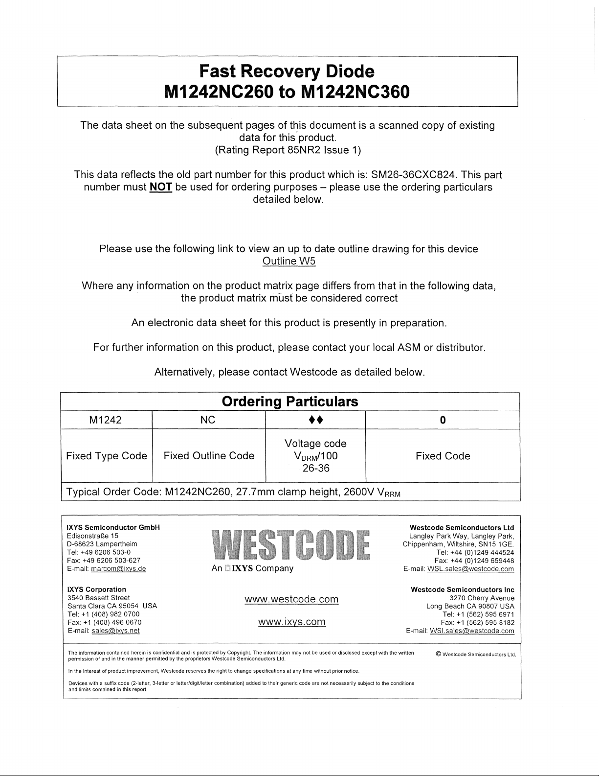
Fast Recovery Diode
M1242NC260 to M1242NC360
The data sheet
on
the subsequent pages
data for
of
this document is a scanned copy of existing
this·product.
(Rating Report 85NR2 Issue 1)
This data reflects the old part number for this product which is: SM26-36CXC824. This part
number must
NOT be used for ordering purposes - please use the ordering particulars
detailed below.
Please
use the following link to view an up to date outline drawing for this device
Outline W5
Where any information
An electronic data sheet for this product
For further information
on
the product matrix page differs from that
the product matrix
on
this product, please contact your local ASM or distributor.
must be considered correct
is
presently
in
the following data,
in
preparation.
Alternatively, please contact Westcode as detailed below.
Ordering Particulars
M1242 NC
••
Voltage code
Fixed Type Code Fixed
Outline Code V
ORM
/100
26-36
Typical Order Code: M1242NC260, 27.7mm clamp height, 2600V V
IXYS Semiconductor GmbH
Edisonstral1e 15
0-68623
Lampertheim
Tel:
+496206503-0
Fax: +49 6206 503-627
E-mail: marcom@ixys.de
IXYS Corporation
3540 Basset! Street
Santa Clara
Tel:
Fax:
E-mail: sales@ixys.net
The
permission
In
the
Devices
and
CA
+1
+1
information contained herein
interest
with
limits
95054
(408) 982 0700
(408) 496 0670
of
and in
the
manner
of
product
improvement,
a suffix
code
contained
(2·letter, 3-letter
in
this
report.
USA
is
confidential
permitted
and
is
protected
by
the proprietors
Westcode
reselVes
or
letter/digitlletter combination)
An
Westcode
the
right
ES
aIXYS
by
Company
www.westcode.com
www.ixys.com
Copyright.
The
information
Semiconductors
to
change
added
Ltd.
specifications at
to
their
generic
may
any
not
be
time
code are
DE
used
or
disclosed
without
prior notice.
not
necessarily subject
except
to
0
Fixed Code
RRM
Westcode Semiconductors
Langley Park Way, Langley Park,
Chippenham, Wiltshire, SN15 1GE.
E-mail: WSL.sales@westcode.com
E-mail: WSl.sales@westcode.com
with
the written
the conditions
Tel: +44
Fax: +44
Westcode Semiconductors
3270 Cherry Avenue
Long Beach
Tel:
+1
+1
Fax:
©
Westcode
ltd
(0)1249 444524
(0)1249659448
Inc
CA
90807
(562) 595 6971
(562) 595 8182
Semiconductors
USA
Ltd.
Page
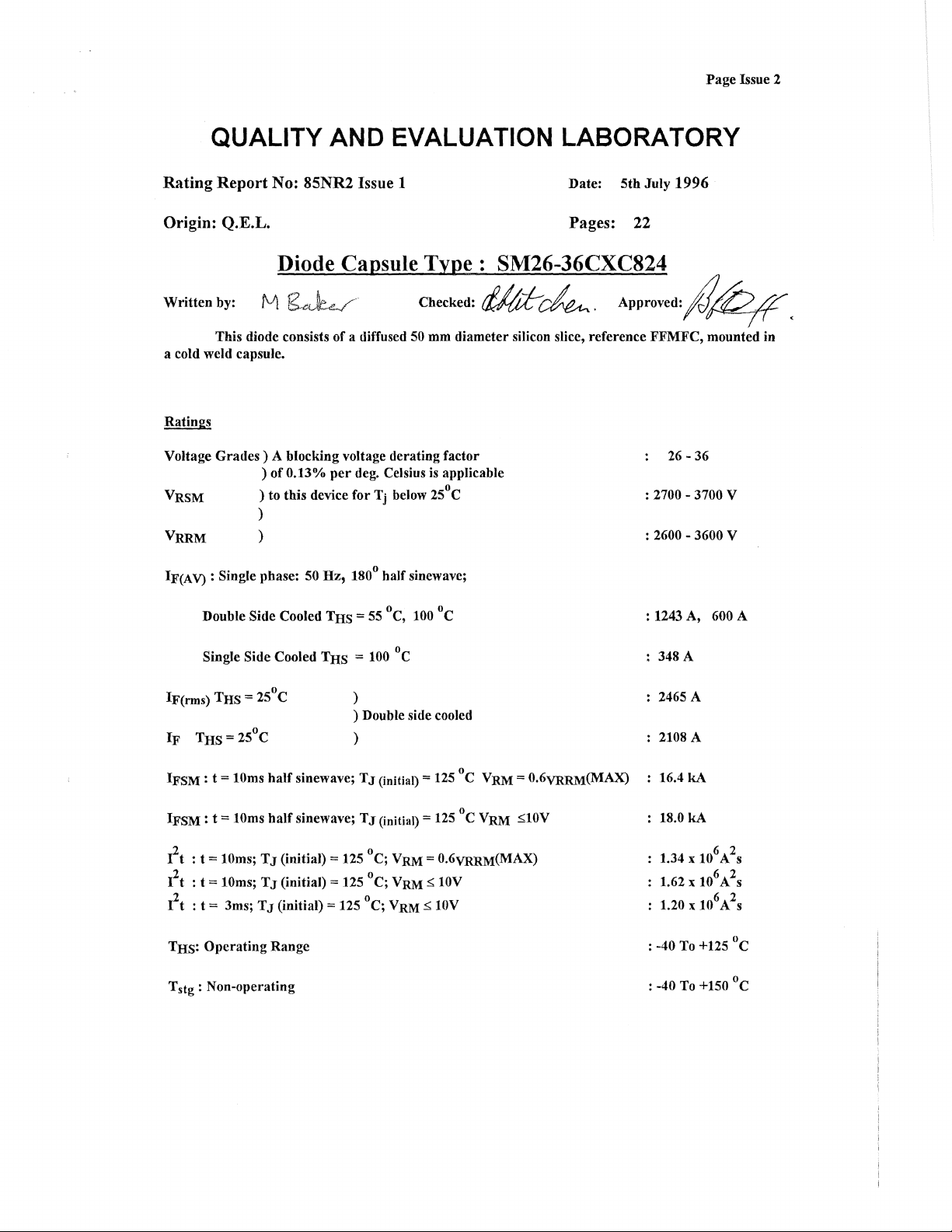
QUALITY AND EVALUATION LABORATORY
Issue 2
Rating
Origin: Q.E.L. Pages: 22
Written
a cold weld capsule.
Voltage
VRSM ) to this device
VRRM )
IF(A
Report
No: 85NR2 Issue 1
Diode Capsule
by:
M
~b./
This diode consists of a diffused
Grades)
V) : Single phase: 50
Double Side Cooled
A blocking voltage derating factor
)
of
0.13%
per
)
Hz,
180° half sinewave;
THs
50 mm diameter silicon slice, reference
deg. Celsius
for
Tj below 25°C
=
55°C,
Date:
Type:
SM26-36CXC824
Ch"k'd,rtIti-~.
is
applicable
100°C
5th
APProwd,!q.
July
1996
FFMFC,
2700 - 3700 V
:
: 2600 - 3600 V
: 1243 A, 600 A
26
- 36
mounted in
Single Side Cooled THS =
IF(rms) THS = 25 C
IF
THS=25
IFSM : t = 10ms
IFSM:
t = 10ms
rt
: t = 10ms;
rt
: t = tOms;
rt
: t = 3ms;
THS:
Operating
Tstg:
Non-operating
°
°
C
half
half
TJ
TJ
TJ
(initial) =
Range
(initial) =
(initial) =
sinewave;
sinewave;
125°C;
125°C;
125°C;
100°C
)
) Double side cooled
)
TJ
(initial) =
TJ
(initial) =
125°C
125°C
VRM
= 0.6VRRM(MAX)
VRM
s::
10V
VRM
s::
10V
VRM = 0.6VRRM(MAX)
VRM
S::10V
348 A
2465 A
2108 A
t6.4
kA
18.0
kA
1.34 x 10 A s
1.62 x 10 A s
1.20 x 10 A s
: -40 To +125 °c
: -40 To +150 °c
6 2
6 2
6 2

Page
No
Page Issue 2
R.R.
No
85NR2
R.R. Issue 1
2
Characteristics
A :
TJ=
2SoC
B :
TJ=
2SoC
C :
TJ=
2SoC
D
:TJ=2SoC
A)
B)
VF = A + B.ln(iF) + C.iF + D
(Maximum values unless otherwise stated)
..J
iF
C )
D )
VFM
at
IFM = 2200 A
Rth(J-HS) Double side cooled ) Steady-state d.c. and
IRRM :
Vfr :
Single side cooled ) 1
at
VRRM(MAX)
at
diF/dt =
~
a.c. resistive load.
:
1.27V
:
0.420mQ
2.20 V
0.022 KfW
0.044KfW
60mA
Reverse recovery
diRldt = 60 Allls;
QRR
(total area)
QRA
(SO%
chord)
trr
(SO%
chord)
IRM
Mounting Force
Outline Drawing
JEDEC
Outline
NOTE:
at
IFM = 1000 A; tp = 1000
VRM
= 50 V
No.
All characteristics arc at
IlS
: 810 IlC
: 100A249
: DO-200AC
TVJ
= TJrnax operating unless stated otherwise.
8
Ils
19 -26
kN
(1900 - 2600 kg.!)
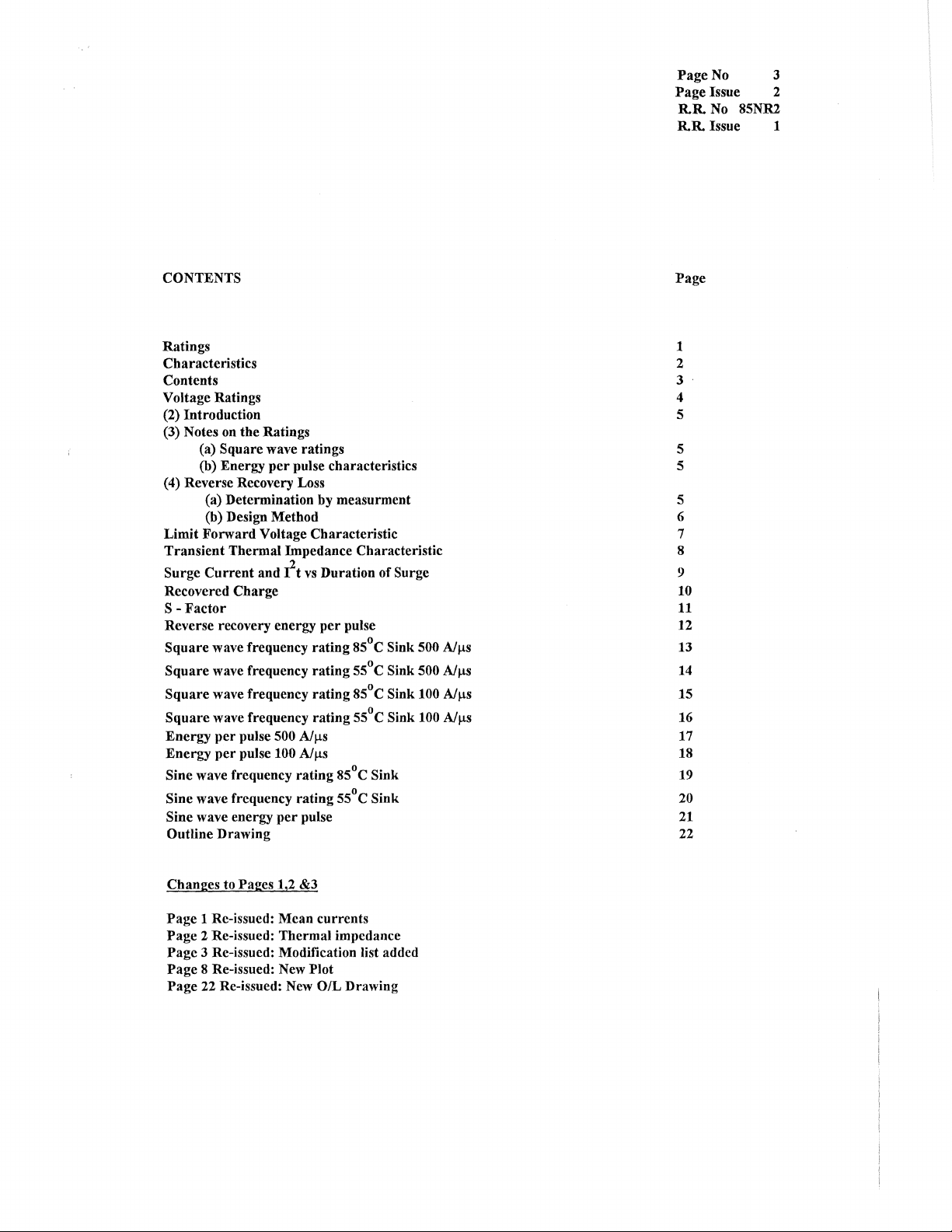
Page
No 3
Page
Issue 2
R.R.
No
8SNR2
R.R. Issue 1
CONTENTS
Ratings
Characteristics
Contents
Voltage Ratings
(2) Introduction
(3) Notes on
(4) Reverse Recovery Loss
the
Ratings
Square wave ratings
(a)
(b) Energy
per
pulse characteristics
(a) Determination by measurment
(b) Design Method
Limit
Forward
Transient
Surge
Current
Voltage Characteristic
Thermal Impedance Characteristic
and
rt
vs
Duration of Surge
Recovered Cbarge
S -
Factor
Reverse recovery energy
Square
Square
Square
Square
Energy
Energy
wave frequency
wave frequency
wave frequency
wave frequency
per
pulse
per
pulse 100
Sine wave frequency
Sine
wave frequency rating S50C Sink
Sine
wave energy
SOO
per
per
rating
rating
rating
rating
A/f.lS
A/f.lS
rating
pulse
Outline Drawing
pulse
85°C Sink 500
SSoC
Sink
85°C Sink 100
SSOC
Sink
85°C Sink
SOO
100
A/f.lS
A/f.lS
A/f.lS
A/f.lS
Page
1
2
3
4
S
S
5
S
6
7
8
9
10
11
12
13
14
15
16
17
18
19
20
21
22
Changes to
Page
Page
Page
Page
Page
Pages 1,2 &3
1 Re-issued: Mean currents
2 Re-issued: Thermal impedance
3 Re-issued: Modification list added
8 Re-issued:
22
Re-issued: New OIL Drawing
New
Plot
- 4 -
Voltage
Ratinqa
Voltage
26
28
30
32
34
36
ClaBo
V
HIH"l
V
2600
2800
3000
3200
3400
3600
Vl1sr~
V
2700
2900
310b
3300
3500
3700
8upply
This
l1a8
neport
been
i8
applicablo
agreed
to
by
Salea/Production.
l1iqher
or
lovlOr
voltago
gradED
wllCn
2.0
INTRODUCTION
The
diode
all
diffuoed
characteristics
3.0
NOTES
(a)
Square
silicon
ON
series
with
THE
comprises
81icos.
good
RATINGS
wave
ratin9s
"5"
- 5 -
fast
All
theso
factors.
recovery
diodes
cold-weld
hove
controlled
capsules
with
reverse
recovery
forward
(b)
obtained
4.0
On
voltage,
Tho
following
reverse
reverse
waveform
evaluated
These
Energy
These
Let:
Then
and
REVERSE
account
no
recovery
(a)
Determination
From
(sce
Note
ratings
current
per
curves
for
Ep
width,
W
AV
conditions
be
=
are
of
100
pulse
enable
the
in
Ep
x
given
characteri.8tic8
Energy
JOUles.
f.
TSINK = TJ(MAX) - W
RECOVERY
of
allowance
procedure
the
LOSS
number
for
is
reverse
recommended
loss.
by
Measurement
waveforms
1)
and
recovery
be
fI
joules
of
reverse
1000
per
recovery
waveform
from:
and
rapid
not
of
voltage
pulse.
for
leading
500A/uS.
estimation
covered
per
pulse
Rth
AV
circuit
recovery
current
must
by
for a given
variables
loss
for
use
preDcnt
be
A
nC\'i
edge
linear
of
device
the
frequency
affecting
has
been
where
obtained
during
constructed.
heot
sink
rates
dissipation
ratings.
current
reverse
made
it
is
necessary
from a high
recovery,
Let
temporoture
of
rise
and
pulse
in
these
Frequency
on
instantaneouo
the
area
con
of
to
be
recovery
ratings.
to
include
unrler
tilDn
shunt
this
bD
t
duration
A
Area
f =
rated
The
total
W(TOT)
T SINK
I
w lOre r
under
=
':i(
(new)
=
4.11 x 10
t
of
reverse
reverse
frequency
dissipation
..
orlglna
1)
at
is
+ Axf
-5
recovery
loss
waveform
the
original
now
given
loss
by
per
per
heat
pulse
pulse
sink
in
microseconds
in
joules
temperature
(W.S.)
NOTE
- 6 -
1
REVERSE
This
recovery
that:
(a)
(b)
(c)
(b)
Design
In
conditions,
from
curves
Let
page
12
RECOVERY
device
current.
a.c.
coupled
affected
The
measuring
100
screen
without
Measurement
out
with
series
Method
circumstances
or
for
on
page
E be
the
)
LOSS
BY
MEASUREMENT
has 8 low
When
measuring
devices
by
prior
oscilloscope
heights
ov~rload.
of
reverse
an
appropriote
connected
where
design
12
value
of
reverse
such
passage
-
to
across
,
it
is
purposes,
energy
recovered
the
charge
as
current
of
hi~)h
has
cope
recovery
silubber
diode
not
possible
the
per
reverse
charge
care
amplitude
adequate
with
the
voltage
of
anode
additional
end
must
transformers
dynamic
initial
waveform
.22
uF
to
cathode.
to
measure
losses
cycle
in
peak
reverse
be
taken
are
forward
current.
rango -typically
forward
should
ond lOohms
voltage
may
be
joules
to
ensure
not
current
be
in
and
estimated
(curves
carried
current
on
Let
ThenT
Where TSINK new
original
f be
SINK
is
the
operating
(new) ( ) E R f
~
is
the
heat
sink
frequency
TSINK
the
required
tempereture
original
in
Hz
- x
maximum
given
wi
th
heat
th
x
sink
the
temperature
freq'uency
Bnd TSINK
ratings.
- 7 -
(fJ
ll!
0:
W
0..
L
<t
"
I-
Z
LJJ
0:
0:
::J
U
0
0:
<t
3:
0:
0
lJ...
(fJ
::J
0
W
Z
<t
I-
Z
<t
I-
(fJ
Z
H
10000
5000
3000
1000
500
300
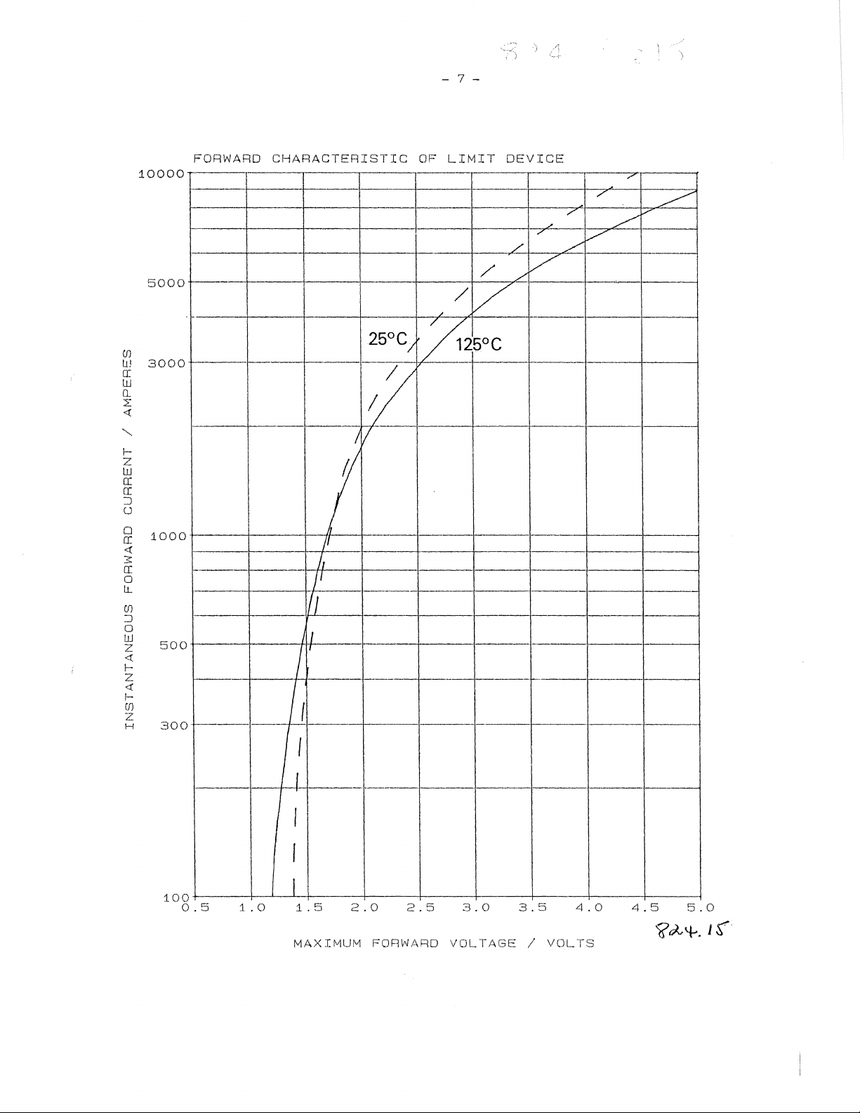
FORWARD
CHARACTERISTIC
25°C;
1
,/
!
/'
/,
/1
/J
III
/
II
I (
OF
LIMIT
/
DEVICE
..-
'"
./
./
./
/'
""
,/
/"
/
V
~25OC
'"
~
/V
100
0.5
1.0
I
I
I
I
1.5
MAXIMUM
2.0 2.5
FORWARD
3.0
VOLTAGE I VOLTS
3.5
4.0
4.5
5.0
 Loading...