

Page 1
Soft Recovery Diode
Types
The data sheet
on
M0437WC080 to M0437WC140
the subsequent pages
of
this document is a scanned copy of existing
data for this product.
(Rating Report
80NR1 Issue
3)
This data reflects the old part number for this product which is: SM02-14CXC 170.
This part number must NOT be used for ordering purposes - please use the ordering
particulars detailed below.
Limitations of this data are as follows:
This device is only available for grades
08 to 14 (800V to 1400V V
RRM
)
The following link will direct you to the appropriate outline drawing
Outline
Where any information on the product matrix page differs from that
W1
in
the following data,
the product matrix must be considered correct
in
An electronic data sheet for this product is presently
For further information
on
this product, please contact your local ASM or distributor.
preparation.
Alternatively, please contact Westcode as detailed below.
Ordering Particulars
M0437 wc
Fixed Type Code Fixed
Outline Code V
Typical Order Code: M0437WC140, 14mm clamp height, 1400V V
IXYS Semiconductor GmbH
Edisonstra~e
D-68623 Lampertheim
Tel:
+496206503-0
Fax:
E-mail: marcom@ixvs.de
IXYS Corporation
3540 Bassett Street
Santa Clara
Tel:
+1
Fax:
E-mail:
The information contained herein
permission
In the interest
Devices with a suffix code (2-letter, 3-letter or letter/digitlletter combination) added
and
limits contained
15
+496206503-627
CA 95054 USA
(408) 982 0700
+1
(408) 496 0670
sales@ixys.net
is
of
and in the manner permitted by the proprietors
of
product improvement, Westcode reserves the right to change specifications at any time without prior notice.
in
this report.
confidential and is protected by Copyright. The information may not be used
An
Westcode
E
CIXYS
www.westcode.com
Semiconductors Ltd.
Ie
Company
www.ixys.com
to
their generic code are not necessarily subject
or
••
Voltage code
RRM
08-14
E
disclosed except with the written
/100
RRM
to
the conditions
0
Fixed Code
Westcode Semiconductors
Langley Park Way. Langley Park,
Chippenham, Wiltshire, SN15 1GE.
E-mail: WSL.sales@westcode.com
E-mail: WSl.sales@westcode.com
Tel: +44 (0)1249 444524
Fax: +44 (0)1249659448
Westcode Semiconductors Inc
3270 Cherry Avenue
Long Beach CA 90807 USA
+1
(562) 595 6971
Tel:
Fax:
+1
(562) 595 8182
© Westcode Semiconductors Ltd.
Ltd
Page 2

QUALITY
EVALUATION
LABORATORY
Rating
Origin:
Written
This
diameter
ThiS
Report
Ratings
Voltage
V
RSM
VRRM
IF(AV)
IF(rms)
:
T
Operating
HS
T't;
s g
Report:
diode
silicon
Grades
:
Single
Double
Single
T
HS
T
HS
.t
=
t
=
t
=
t
'::::
t
=
Non-operating
80NR1
Diode Type
consists
supersedes
phase;
Side
Side
= 25°C )
° ) Double
= 25 C )
10ms
half
half
10ms
1
Oms;
10ms; T
3ms; T
Range
slice
Cooled
Cooled
T
J
J
J
(Issue
SM02-14:CXC170
of a diffused,
mounted
Rating
50 Hz,
THSE = 55°C,
THS
sinewave;
sinewave;
(initial
(initial)
(initial
~)
Checked:
in a cold
report
1800 half
= 100°C
side
cooled
T
(initial)
J
T
(initial)
J
'=
125°C;
= 125°C; V
=
125°C;
MN)
fast
weld
80NR1!
sinewave;
100°C
V
RM
RM
V
RM
recovery
capsule
(Issue
::::
125°C;
=
125°C;
::::
0.6V
f
10V
~
10V
Date:
Pages:
Approved:
24
housing.
2).
(Converter
V
RM
V
RM
(MAX)
RRM
18th
November, 1991
22
/l};
(rJj5;z::4:t'.
mm
Ratings)
=
O.6V
RRM
10V
,\/1
""~)",
02-14
300~1500V
200·-1400V
438A,
114A
S80A
727A
(MAX)
I 4500A
4950A
1.01
1.22
0.91
-40
-40
i'
to
to
202A
x 105
x 10
x 10
+125'
+150'
:
A
5
A:
5
A:
Page 3
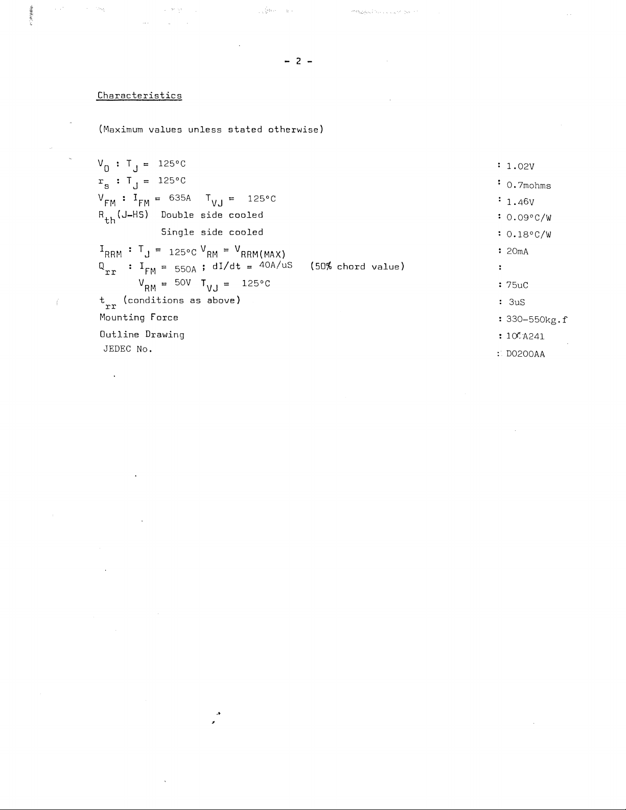
Characteristics
- 2 -
(Maximum
T
Vo
r T
V
s
FM
:
J
J
IFM
Rth(J-HS}
IRRM
Q
rr
t
(conditions
rr
Mounting
Outline
JEDEC
No.
values
125°C
125°C
:::
Double
Single
T J
'"
IFM
:=
V
:=
RM
Force
Drawing
unless
635A
TVJ
side
side
125°
C V R M
550A ; dI/dt
50V T VJ:=
as
above)
stated
'"
cooled
cooled
==
V R R M (
125°C
otherwise)
125°C
MA
X )
= 40A/uS
(50%
chord
value)
1.02V
O.7mohms
1.46V
O.OgoC/W
O.18°C/W
20mA
75uC
3uS
330-550kg.f
10l':A241
:.
D0200AA
.>
Page 4
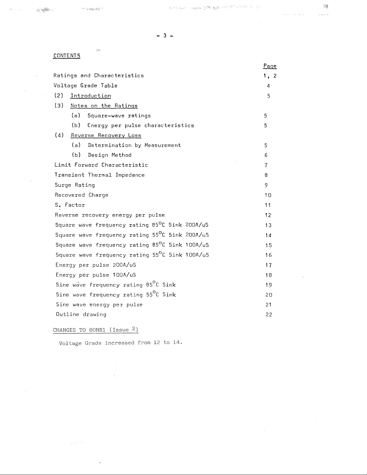
CONTENTS
Ratings
Voltage
(2)
Introduction
(3)
Notes
(a)
(b)
(4)
Reverse
(a)
(b)
Limit
Forward
Transient
Surge
Rating
Recovered
S.
Factor
Reverse
Square
Square
Square
Square
Energy
Energy
Sine
wave
Sine
wave
Sine
wave
Outline
and
Characteristics
Grade
on
Table
the
Square-wave
Energy
Recovery
Determination
Design
Characteristic
Thermal
Charge
recovery
wave
frequency
wave
frequency
wave
frequency
wave
frequency
per
pulse
per
pulse
freqwency
frequency
energy
draWing
Ratings
ratings
per
pulse
Loss
Method
Impedance
energy
rating
rating
rating
rating
200A/uS
100A/uS
rating
rating
per
pulse
- 3 -
characteristics
by
Measurement
per
pulse
8SoC
SSoC
8SoC
5SoC
85°C
55°C
Sink
Sink
Sink
Sink
Sink
Sink
200A/uS
2001l/uS
1DOA/uS
1
DOA/uS
Page
1 ,
4
5
5
5
5
6
7
8
9
10
11
12
13
14
15
16
17
18
19
20
21
22
2
CHANGES
Voltage
TO
80NR1
Grade
(Issue
increased
2)
from
12
to
14.
Page 5
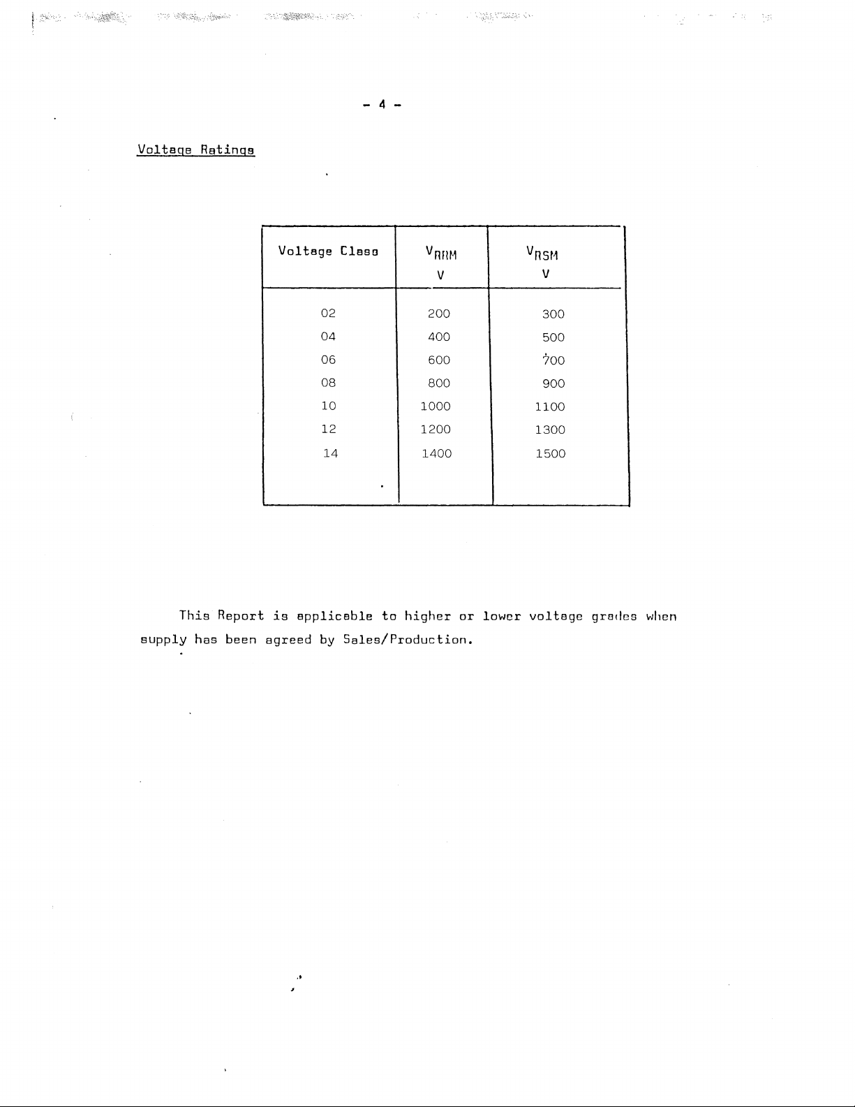
- 4 -
Voltage
Ratings
Voltage
02
04
06
08
10
12
14
Claso
V
nflM
V
200
400
600
800
1000
1200
1400 1500
Vnsr~
V
300
500
700
900
1100
1300
supply
This
has
Report
been
is
applicable
agreed
,.
to
by
Sales/Production.
higher
or
lower
voltege
grades
when
Page 6
2.0
INTRODUCTION
The
diode
all
diffused
characteristics
3.0
NOTES
(a)
Square
silicon
ON
series
with
THE
comprises
slices.
good
RATINGS
wave
ratings
"S"
- 5 -
fast
All
these
factors.
recovery
diodes
cold-weld
have
controlled
capsules
with
reverse
recovery
forward
(b)
obtained
4.0
REVERSE
On
voltage,
The
following
reverse
(a)
(see
reverse
waveform be A
evaluated
These
ratings
current
Energy
These
curves
for
Let:
Ep
width,
Then W
AV
and TSINK =
RECOVERY
account
no
of
allowance
procedure
recovery
Determination
From
waveforms
Note
1)
recovery
from:
of
per
pulse
enable
conditions
be
the
in
=
Ep x f.
TJ(MAX)
LOSS
the
number
for
loss.
and
reverse
loss
joules
are
given
200
and
for
100A/uS
characteristics
rapid
not
covered
Energy
per
joules.
- W
AV
of
circuit
reverse
is
recommended
recovery
by Measurement
of
recovery
voltage
waveform
per
pulse.
leading
estimation
by
pulse
for a given
Rth
variables
loss
for
use
current
present
must
be
A
new
edge
linear
of
device
the
frequency
affecting
has
been
where
obtained
during
constructed.
heat
sink
rates
dissipation
ratings.
current
made
it
is
necessary
from a
recovery,
Let
temperature
of
and
reverse
in
these
high
an
the
rise
of
to
be
pulse
recovery
ratings.
to
include
frequency
shunt
instantaneous
area
under
can
then
be
this
where r
t =
duration
A Area
f =
rated
The
total
W - W + Axf
(TOT)
-
=
t
of
reverse
under
reverse
frequency
dissipation
(original)
.>
at
recovery
loss
the
is
waveform
original
now
given
loss
by
per
per
heat
pulse
pulse
sink
+
Rth x f)
in
microseconds
in
joules
temperature
)
(W.S.)
Page 7

NOTE
- 6 -
1
REVERSE
This
recovery
that:
(a)
(b)
(c)
(b)
Design
In
conditions,
from
curves
Let E be
page
12)
RECOVERY
device
LOSS
hes
current.
a.c.
coupled
affected
The
measuring
100
screen
without
Measurement
out
with
series
connected
Method
circumstances
or
for
on
page
the
BY
MEASUREMENT
e low
When
reverse
measuring
devices
by
prior
passage
oscilloscope
heights -to
ov~rload.
of
reverse
an
appropriate
across
I
where
design
12.
value
it
purposes,
of
energy
the
such
cope
recovery
snubber
diode
is
not
per
recovered
charge
as
current
of
high
has
adequate
with
anode
possible
the
additional
reverse
cherge
care
transformers
amplitude
the
voltage
of
0.1uF
to
to
cycle
end
must
dynamic
initial
waveform
cathode.
measure
losses
in
peek
reverse
be
taken
are
forward
current.
range -typically
forward
should
and
10
ohms
voltage
may
joules
to
not
current
be
in
and
be
estimated
(curves
ensure
carried
current
on
Let f be
Then
Where TSINK new
original
is
the
operating
T (new) ( ) R
SINK
. = TSINK
is
the
heat
sink
frequency
original
the
required
temperature
in
Hz
- E x
maximum
given
heat
with
th
x f
sink
temperature
the
fre~uency
and
ratings.
TSINK
Page 8
- 7 -
en
Cl.
::r
«
"'-
IZ
LV
II
II
::l
tJ
0
II
«
~
II
0
u..
en
::l
0
LV
Z
«
IZ
«
I-
en
Z
H
10000
5000
3000
1000
500
300
I-
1--
FORWARD
-
25
Q
~/
II
/
/
/
II
CHARACTERISTIC
I
I
./
/
/
/
/
/
1/
/
V
/
25
Q
V
/
/'
OF
r;;
l;=
LIMIT
t/
-
DEVICE
~~
V
I
~
--
-
------.:
~
100
1.0
il
1.2
MAXIMUM
1.4
INSTANTANEOUS
..
1.6
1.8
FORWARD
2.0
VOLTAGE / VOLTS
2.2
2.4
Page 9

:'{:
·:r
l-
I-
<!
3::
U
"
O~
W
U
Z
<!
0
W
n.
;:[
H
..J
<!
;:[
cr
W
I
II-
z
W
H
en
Z
<!
cr
I-
1.0
0.1
0.01
JUNCTION
l-
f--
I-
~-
:.
--
I
I 1
.-
l-
--
I-
1
---
TO
j-
.....
l---"
HE~T
I
[.....---'
SINK
~i""
L,..o
TRANSIENT
I
-----
THERMAL IMPEDANCE
1
_____
----
L-----
-r-
-tt-
I
I
I
-I-
T
g.180
C/W
0.090
°C/W
CD
~
~
~
.......v
-
L
C
~
I
t-'"""
-
~-
I
0.001
.
0.001
I
I I I
II
II
0.01
h
J
I I I , , 1,1
I
TIME
0.1
(SECONDS)
I
I I I III"
1.0
, I I I ! , ,
I
10.0
Page 10

1
I
:;(
2S
::J
u
W
U)
a:
::J
en
w
z
I-l
en
LL
-1
<{
:c
::L
<l:
W
Q
-1
<{
}-
0
}-
)-
z
w
a:
a:
100
10
lL
~
....................
------
--
------
1
MAXIMUM
---
I
-.........,
><
K
~
I
I I
I
3 5
--
-.......
...
A--
-----
---
-----'-.....
NON
......
I
I
i
:-l--
I !
REPETITIVE
I
I
10
SURGE
CURRENT
I
I
vV
vV
/'
/
V
V
V
V
/
::::::--
I---
----
t:::r--.
--
--
I
I
1 5
AT
INITIAL
/
~
~
/
~
~
10
JUNCTION
I~
(I
It:
n
//"
.......
V
V
t::--
b-:
-I-
TEMPERATURE
.C)
'"
.
...-
V
V
~
50
1250C
6
10
/"
IT
c.
/'
/'
~u:;vr
II
SM'
VRR~
(I
SM:
60~\
L
100
hi
0
If
M
__
l
,
,
C0
U
w-
U1
0J
en
10
10
Q
::!':
~
5
.LJ
(\j
I-l
::!':
::J
::!':
H
X
<{
::!':
4
(0
I
I
DURATION
OF
SURGE
~s)
DURATION
OF
SURGE
(cycles
at
50
Hz)
Page 11

-
10
-
MAXIMUM
200
Ul
CO
L
100
0
..J
:J
0
U
0
cr
U
H
L
L
L
el
~
W
t9
cr
<1:
I
U
0
W
cr
W
>
0
U
W
cr
9
8
7
6
5
4
RECOVERED
i~
II'
V./'
,/
/
~
vV'
V
V
1/
~V
0~
vV'
VV
V
V
1/
CHARGE
./
V
V::
~
V
V
V
V
./'
)/
v
AT
V
V
V
,/
V
V
125°C
",v
./
v
:.....-
vV'
vI-
vV
V
JUNCTION
V
V
V
v
V
....
f.--
~
~
1--/
~
./
V
V
'"""'"""
V
TEMPERATURE
~OOOA
V
v
V
l-
V
I-
I---"
-
MIN.
f-
f--
CONFIDENCE)
400A
200A
~OOA
AT
(95%
400A
3
20
V
20
..
l/
/
3
COMMUTATING
4
5 6 7 8 9
di!dt
100
AMPS!~s
200
Page 12

z
o
H
I-
Li
z
f\
1\
.'\
'\
\
-
11
'\
'\
-
(
U
/)"
" ,
u
:1..
W
.D
,,-
CL
<f.
I
.-!
Cl
LLI
n-
u
W
-::;,
~
'.
Lu
c.:
l
z
rul~
-
f-
f-
H
IT:
0
f-
U
---
<i
LL
=
([J
=
-/
.-!
.-!
"
" H
0
---
"
lfl
ru
~
f-
I"
-/-
-rl
f-
l-/
G
..
.,-l
T I
0'1
0
i:::iDJ
~
GJ
0
:J
\l.=j
S
r~
\
1\
f\
f',
0
f\
.iJ
0
Page 13

MAXIMUM
REVERSE
RECOVERY
ENERGY
LOSS PER PULSE,
12S
o
~UNCTION
C
TEMPER4TURE
SNUBBER
PEAK
-:;:::::?
....-
W
Ul
....J
:::J
0..
IT
w
0..
Ul
W
....J
:::J
0
J
H
....J
....J
H
~
300
100
3
20
g
8
7
6
5
4
2
20
~
...-
....-
;.
-;::::---
~
.....-
,'"
REVERSE
b:::
--
~
V
I--
....-
--
VOLTAGE
~
p
f--
:..-
4
---::::
,.........
---
--
CONNECTED
VRM -0.b7
::.--
...-
~
-
-
---
-
..-
5
-
6
O.10~F
O~
>--
-
-
l...-
7 8
10
HIGHEST
-
-
>--
i-"
g
OHMS
GRADE
I.---
--
-
---
100
-
~
-
-
VOLTAGE
--=====
*
-
-
~
I--
-
200
10004
400l,
200A
100A
-
N t
*
NOTE:
ENERGY
PER PULSE
SHOULD
COMMUTATING
BE
AD~USTED
dl/dt
PRO
AMPS/~s
RATA
WITH
APPLIED
PEAK
RECOVERY
VOLTAGE
Page 14

T
-
13
SINK
-
85°C.
200A/~s
N
I
>u
Z
w
:J
o
W
cr
LL
100K
10K
1K
100
10
P>.--
f-
f-
f-.
10,us
'\
'\
1\
,
\
\
\
\
\
i'\
1\
'\.
1\
1\
\
,
r\
1\
\
f\
\
1\
\\
\\
1\
~
f\
~
1\
1\
\
!\
'\.,.
~
\
I~~
IV<
I~~
1<
1\
~
I\i(
~
.,(
"
'\
'"
'\
1,\
1\
"'\
1\
",\
1\
'\
'\
'\
\
"
\
1\
~
'\
\
"
~\
i\
~\
\
\
\ \
-
\
"
\
1\
\
\
100,us
PULSE
V.>
'\:
I~~
\
1\
1\
f\
I'\:
1\
1\
[\
'\
\
1\
f\
\
1\
\
\
1\
\
1\
1\
1\
WIDTH
I~
_'\
"
\
1\
[\\
f\\
1\\
1\
"\
'\
'\
\
\
\
~
1ms
1'\
1\
'\
1\
1\
'"
1,\
1\
\
1\
\
f\
1\
\
'\
1\
h
\
1\
1\
1\
\
1\
\
1\
1\
10ms
..
Page 15

T
-
14
SINK
-
55°C.
200A/ps
N
I
>-
U
Z
W
:J
CJ
W
IT
LL
lOOK
10K
lK
1'------
------
-1---
--
=-C
=_~~_~~
------\::
-----~-
-
------
--+I\-,\,---~
_____
-----1'--\--t\:--j--j\+t-N+-----
~-
~
---
-----
--
==-
1=-
f----~ --
---- --c-- - -
\
~
-\ -----------
~
\ \
1\
[\
f\
~-\---
~
--\1-\
-.
~~
~~
'\
\
c
~~~,'
--
r---l,\J~
--1-
\'
- -
~--
-\1\
-------
-----------
= = -_
~~~-_~~
- -
-
1\
1\
-
,
1\
-
__
=~
---
----
---
f----
----I------------ ---------
1-------
---,-
------------1--
-------f----
~------t-
t-----.
c--,\--t-
~~~~~=~.--t-----t---+-++-+-I
°A \ \:-
------ ---------
___
-,=-~-__ _ __
----
__
___ _ __
--------
____
__
__
__
--
f--
-
~\~;~c,:
-I~
~-.y:[\--I-C's--I~
~\l~\
-
)r\
-----
\ - \
1\
-----------
~~~~
_ ________
r-------
_ ___________________ _
- --
j--------
+----
-------
---
---
____
---
---- - ---
----~t_-
___
-=-=
__
_____
----_
,-
- - -
--
-
- -- --_
,--
f';
---1----
-------1----
-
lS.~\
--1--
--'---
r--
--
--
__
_
-
=:
--
__
_
-
100
10
y
\
r--t---+-+-+++-H+-
__
-r-r--++~+~I---~_---=~\~~r++I\~~\-T~\+-~I\~~
\ \
1\
1\
1\
\
100f1s
PULSE
WIDTH
lms
\.
\.
\1\
\ f\
\
1\
\
1\
r\
10ms
Page 16

N
I
>-
u
Z
W
:J
CI
W
(I
lL
100K
10K
1K
100
10
\
\
\
1\\
\
\
1\
\
\
r'\
1\
~
,\
\.
1\;
\
\
1\
1\
1\\
1\
\
~~
I
i
T
SINK
I
,
-
\
II
1
I
85°C.
100A/~~
}-
0
'I
1\1\
y\
,
Y\
\
:s..
'\
~
"P'.>
\
\1\
\,
\
\ I
\:
1\
I
1
\:
I
'\
t>
~,
[\
[\
\.1
,
1
1\
1\
\
\
\
1\
f\
~
\
I
;
i
"
\
;
1\
1
1\
1\
1\
WIDTH
"\
,
\
1\
i\
\.
\
\
\
1\
~\
1\
~\
\
~
1\
\
\
\
\
\
\
\
1\
\
\
1ms
\
1\
r\
'\
\
\
\
I'
\
\
\
\ I
1\
\
\
\
f\
i
\.."
I
\.
v~
\
~...,.\
1\
I\~
IY"O~
1\
I~I{O...,.
I
\'-:
~
""...,\.'
I
1\
'0\
O~
1\
I
\)J~
1 \
i \ .
I\~
i i
II
I~l\
I
,
i:
i !
i
I
i
,
I
!
I'
,
!1
I
I
I
100f-ls
PULSE
"0.
1\
10ms
.>
Page 17

100K
10K
>-
u 1K
Z
lJJ
:J
Ci
lJJ
cr
lL
100
10
10,us
,
,
\
\'
1\\
l'<
1\
~
'I.
\\
1\
\
T
SINK
\
1\['-
1\
1\
'.7
~
1\
\
[\
I~
1\
~I\
I\~
0).. '\'
~
I\.
I'
-.;,\
0d\
V-.;\
~
~
f'A
-=a
~
~
l\~
~\O~
\).
100,us
PULSE
55°C.
0
~
'\
1\\
~.>
\
1\
I\.
\
1\
1\
\ \ l'-... ,
\
\ \
f\
\
1'\
\
~
\
.V
I,) Y
t;:.\
1\
-0.
>'\
1\
\:
I~~
[\
1\
!'I
1'\
1\
1\
1\
1\
!'I
\
1\
[\
,
,
\
1\
.\
1\
\
100A/ps
1\
WIDTH
\
~
~
0
-'c
\
\
1ms
'\
\
'\
\
'I.
,
\
I'
[\\
\
1\
1,\
\
I\.
1\
\
1\
\
,
\
\
[\1
1\
1\
\
\
1\
1\
\
1\
10ms
..
Page 18

.. -17
-
w
UJ
.-l
::l
0..
II
W
0..
>-
(!)
II
W
Z
W
100
10
J
1 J
100mJ
J
/
1/
-
J
/
/
,/
/
/
V
7
V
/
V
/
/
/
/
/
/
7
/
V
/
J
V
/
V
V
/
V
1/
/
/
/
V
1/
V
1/
IJ
1I
V
II
IJ
1I
II
171
I J
17
I}
/
1I
II
rl
II
V
f
V
~
II
1/
I
~V:
V /
V
/ /
II
'i
V
/ /
/
/ /
/
I
/
II
/
/
V
/
/
/
/
--;
/
V
J
J
V
V
V
V
V
V
J
V~
/
II",
l/
/
VI4
J
VIr.
II
IV
I?
IJ
IJ
IJ
1I
/
VI
/
/
/
1/ /
/
"/
I
V;
/
/
/
/
V
V
10mJ
101-1
/
I
II
V
V
J
/
V
/
V
V
V
V
I/V
/
s
V
1I
/
/
1/
1/
100I-lS
1/
/ /
/
/
/'
/
V
PULSE
/
/
1/
V
/
WIDTH
1ms
I
10ms
..
Page 19

w
(f)
-.l
=>
n..
IT
W
n..
>-
(!)
IT
l!J
Z
l!J
100
...!
10
...!
...!
1
100m...!
10m...!
10fls
II.
rl
/1/
VI
II
IV
V
~
/
II
V 1/
/
II
/
V
V
fl
II
II
/
V
v
1I
II
I
II
V
II
VI
/ V
/ /
II
\I
/
il
1/
/
II;
/
i/
I I
1/
/ /
/
II
/
1I
II
1I
1/
100flS
PULSE
II
L I
\I
II
/
V
V
/
II
/
I
/
/
J
/
I
J
/
/
I
1/
III
;(
/
J
Ii
WIDTH
I
/,
Y
1/
/
1I
I
y
I
V I
II
II
/
/i
/
<
.'
::::'~.
',
•••
i
,
!
II
/
~;I
II \I
~'
pOOh
I,
..
, /
/
/
I/,...~I
O~/
~~
~/
1>0
1/
~
1/
''"'~/
1/
,0
.
I;
V
'i
I h
}V1
Ii
/
i)
I
,
I
I
! I
/1/
~
I
/
0
'/
~~
'"'~
~
lms
,I
V
/
II
/
V
V
/
'I
/'
VI
,
I
7
/
/
1
/
I
/
!/
I
V
/
1/
/
II
V
V
V
1I
1I
/
I
VI
I
YII
i I
i I
I I
I
i
i ,
I
I
I
/
V
/
/
V
1/
i
I
I
I
I
\I
1/
II
1/
10ms
,.
Page 20

I
'-'
>-
U
Z
W
:J
CJ
W
II
il..
..
·.1.:.:·
.
-
19
-
T
SINK
lOOK
\.
'\
\
85°C.
SINE
WAVE
,
\
'\
,
I\.
'\
1\
i\
\.
\
1\
1\
1\
1"-
t\
I
1
h
\.
\.
,
I"\,
\
f\
"\1"
'\°C
\.
1\
v~
t\
1\
~
"
,";-,'\
-("1
\.
'\.
1\
~~
\~
1\
I~~
~
~'""
-",
100,us
PULSE WIDTH
0
"-
~
::.,...>
1\ \
\:
rt'\
\
r\
1\
Ii\.
1<1,
'\
_\.
\.
IY
\
!\
~
IY
"
f\
~\
\
~
~\
1\
\
W\
\
1\
\
I~)
f\
1\
1\
"
\
I\.
[\
"
1\
1\
1\
\
i\
1\
1\
1\
I~
,
\.
\
\
I'\.
0
\
1\
\
1\
1\
1\
1ms
,
'\
\
\.
\
\
i\
'\
1\.\
\
1\
\
\
'\
I\.
1\
\.
1\
'\
1\
'\
\
\"
\
1\
1,\
\
1\
\
1\
1\
10ms
1\
10K
!\..
I"\,
"\.
1\
N
lK
1\
I\..
'"
\
1\
1\
,
-
100
10
10,us
..
Page 21

T
SINK
55°C.
)-
U
Z
W
:J
Cl
W
IT
lL
lOOK
10K
1K
100
'\
'\
\
""'-\
"\
\
1\\
i\
I""
1\
~
'\
I'\.
1'\
'\
[\
1\
r\
"\
""
r\
[\
.'"
1\
r\
r\
r\
r\
1\
1\
"\
\
\
1\
1\
SINE
\.
.>'
'\
'\
'\
""
i\\
[\\
'\
\.
\
\
r\\
\
WAVE
0
'\
()
I"
/
v.;
1\\
··O(
~
~
1'\(
~
1,\
,~
'\
°r~
P~I\
:~
i\c
~
\
\);
~
~
°0
1\
~t>
~
\
r'/\~
1\1'
,
1\
1\
\
'\
.'\.
\
1\\
\
f\
1\
\
~I\
~
1\
1\
[\
1\
1\
I\.
I\.
r\
\
1\
1\
'\
\
\
'\
\
1\
",\
\
f\
1\
f\
1\
\
\
\
'\
\
\1'
1\
1\
1,\
\.
1\
1\
10
10j-ls
lOOps
PULSE
WIDTH
r\\
1ms
\
\
1\
1\
~
\
1\
1\
10ms
Page 22

w
Ul
-1
:J
0..
0:
W
0..
>-
19
0:
W
Z
W
100
10
1 J
100m
J
1/
V
/
1/
V
V
/
I
V
VI
VI
l-
'/
!I
V
./;
V
rj
V
/
/
V
V
/
/
/1
/
V
V
V
/
/ /
/
I
7
V /
/
1/
VI
/
/
/
7
/
I
/
I-
J
/
L
/
V
17
1/
II~
I
J
/
7
/?
V
V
VI~
V
7
7
I
V
1/
V
V
I/~
I
/
/
/~
-
VI
VI
~
V
V/
1/
/
V
I
!I
/
I V
/
/
V
7
V
/
1/
V
'/
VV
/
V
/
V
J
V
V
/
/
V
/ /
/i
/
V
V
V
V
/
/
/
V
V
/
/
V
1/
V
V
V
V
/
1/
1/
V
1/
V
1/
V
IV
II
1/
1.1
V
V
it
/
1/
1/
'I
10mJ
10fls
/
/
/
V
V
7
..
I
V
1I
VI
V
1/
100flS
PULSE
/ /
I
/ /
J
II
V
/
/
/
!/
1/
/
/
/
V
1/
1/
/
V
II
/
WIDTH
1/
1ms
10ms
Page 23

-
22
ON
0.04-
-
ON
WIDE.
CXC300
-1r)(,
CXC
'\,j
.. _ ..
)
CXC3<30
CXC40C
CXC470
-----
CXC134-
CXC144CXC170
CXC174
..
-
..
----
§
INTERNATIONAL
~
G.A.
DWG
~
WEIGHT.
I-
g
FINISH.
C ,. •
~
DEVICE
52
CENTRE
~
DISTRIBUTED
l:5
SURFACES
§
CLAMPING
tr}
MOUNTING: . CLAtv1PING
LINE
OUTLINE
No.
159B100H100-H110.
70
GRAMS
NICKEL
TO
FORCE
OF
LOtA
OVER
WHICH
PLATE
T10N
AREA
DEVICE
==
330-550kgf.
No.
FORCE
HOLES
OF
CONTACT.
IS
DO-200AA
TO
AND
BE
FLAT
CLAMPED
BE
APPLIED
EVENLY
TOL
TO
BE
~~------------------------------------.-----
COMPRESSED
HEIGHT
0.3
MIN.
11519
II
¢3.6/3.5x1.8
DEPTH
IN
IN
2-HOLES,
CATHODE
A~JODE.
MIN.
AI\jD
ONE
ONE
z
(/)
:z:
0
(j)
:>
w
a:::
~
IS
~~
~~
Zz
00
o :c
'f~
Ol~
on::
100
oW~
~n::o
0
........
z
C
:c
0.3
MIN.
11519
e
f<ETP
c
(:I'~
I/OLUTION
PATH
±0.1
"---'
._-----------
.....
··
..
··r-
ffi)iUlm=r-r->!WJl::t11OTr-
TRl
EB
1..-
DWG.
CQMPUE~.Yt!.1H
I
DIMNS.
U'NG
No.
100A241
--~WESTCODESEMICONDUCTOI
BOX
P.O.
TEL
57,
CHIPPENHAM,
02+9
654-1+1.
TELEX
WILTSHIRE,
«751
Wt:SCDE
G.
SN15
TELEFAX
02
OYER
:=
12
MIN.
-E}-
BS
IN
MILLIMETRES.
308.
Page 24

Drawing Number – W1
Outline Number – 100A241
Westcode Customer Services email: wsl.sales@westcode.com Telephone: +44 (0)1249 444524 Fax: +44 (0)1249 659448
Weight 70g
 Loading...