


Westcode Semiconductors M0433WC120, M0433WC200 Data Sheet
Soft Recovery Diode
M0433WC120 to M0433WC200
The data sheet on the subsequent pages
of
this document
is
a scanned copy of existing
data for this product.
(Rating Report
This data reflects the old part number for this product which is:
80NR14 Issue 2)
SM12-20CXC174. This part
number must NOT be used for ordering purposes - please use the ordering particulars
detailed below.
The limitations of this data are as follows:
This device is available for grades 12 to
Please use the following link to view
Outline
an
up to date outline drawing for this device
20 (1200V to 2000V V
W1
Where any information on the product matrix page differs from that
in
the following data,
RRM
)
the product matrix must be considered correct
An electronic data sheet for this product is presently in preparation.
For further information on this product, please contact your local
ASM or distributor.
Alternatively, please contact Westcode as detailed below.
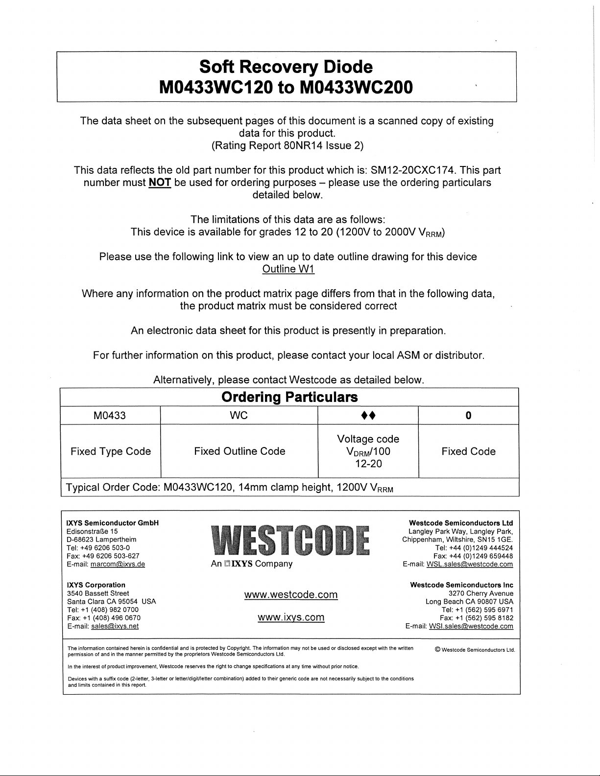
Ordering Particulars
M0433
Fixed Type Code Fixed
wc
Outline Code V
Typical Order Code: M0433WC120, 14mm clamp height,
IXYS
Semiconductor GmbH
Edisonstra~e
0-68623 Lampertheim
Tel: +49
Fax: +49 6206 503-627
E-mail: marcom@ixvs.de
IXYS
3540 Bassett Street
Santa Clara CA 95054 USA
Tel:
+1
Fax:
E-mail:
The
information contained herein is confidential and is protected by Copyright. The information may not be used
permission
In the interest
Devices with a suffix code (2-letter, 3-letter
and limits contained in this report.
15
6206 503-0
Corporation
WESTCODE
An
fHXYS Company
www.westcode.com
(408) 982 0700
+1
(408) 496 0670
sales@ixvs.net
of
and in the manner permitted
of
product improvement, Westcode reserves the right to change specifications at any time without prior notice.
by
the proprietors
or
letter/digiUletter combination) added to their generic code are
Westcode
www.ixys.com
Semiconductors Ltd.
not
••
Voltage code
/100
ORM
12-20
1200VV
or
disclosed except with
necessarily subject to the conditions
RRM
Chippenham, Wiltshire,
E-mail: WSL.sales@westcode.com
E-mail: WSl.sales@westcode.com
the
written
0
Fixed Code
Westcode Semiconductors Ltd
Langley Park Way, Langley Park,
Tel: +44 (0)1249444524
Fax: +44 (0)1249 659448
Westcode Semiconductors Inc
Long Beach
Tel:
Fax:
© Westcode Semiconductors Ltd.
SN15 1GE.
3270 Cherry Avenue
CA 90807 USA
+1
(562) 595 6971
+1
(562) 595 8182
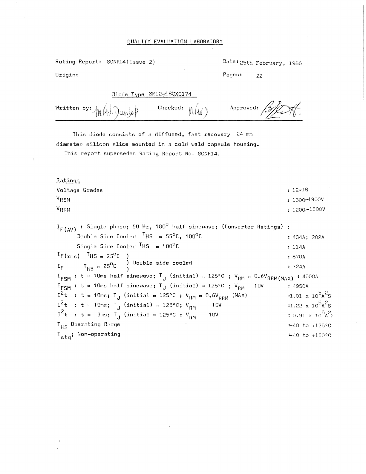
qUALITY
EVALUATION
LABORATORY
Rating
Report:
Origin:
Written
diameter
This
This
report
by:
diode
silicon
Ratings
Voltage
V
RSM
Grades
VRRM
IF{AV} : Single
Double
Single
IF(rms)
IF
I
FSM
I
FSI'4
2
1
t
2
1
t
12t
T
HS
T t ;
s 9
THS:::
T
HS
'"
:::
10ms
t
::
10ms
t
::
10ms;
t
t 1
Omt>
t 3ms;
Operating
Non-operating
80NR14(IsSllC
2)
Diode Type SM12-1.BCXC174
Checked:
consists
slice
supersedes
phase;
Side
Coaled T HS
Side
Cooled
o
2S
C
2S(JC
half
half
T
J
T
;
J
T
J
of a diffused,
mounted
Rating
50
Hz,
THS
Double
sinelrlBvc;
sine\-JQve;
(initial
(initial)
(initial
in
Report
1800 hnlf
==
= 100°C
side
T
J
T
J
:::
125°C
:::
12SoC;
:::
125°C
Ramge
a
cold
55°C,
cooled
(ini
(
initial)
fast
weld
No.
sinel<-Jave.;
wooe
Hal)
;
Vrm
V
.
m
1
.
,
VRf·,
)
/
recovery
capsule
80NR.14.
125°C
'-
125°C
'"
;:
O.6V
10V
10V
Date:
25th
Pages:
APproved:.
24
housing.
(Converter
.
V
,
nr4
.
,
Vm·
(r·1A
rlllt1
February,
22
mm
Ratings)
O.6V
=
10V :
1
X)
1986
fJi
/J".~
..
;/fr,~d
f.~-7f~"
,:;,-----
Rm
<l(r"lAX)
v
12
..
1B
1300-1900V
1200-1800V
:
434A;
114A
870A
724A
4950A
:1.01 x 10
:1.
O
:
:"'40
202A
I
4500A
22 x l05
91
•.
x . ,
to
+150"C
l0
5 0
A'S
A2S
5A2,
Characteristics
- 2 -
(Maximum
T
Vo
r
V fr.l
J
T
J
s
:
In-1
Rth(J-HS)
t
(conditions
rr
Mounting
Ou"Uins
JEDEC
NO.
values
125°C
125°C
.-
635A
Double
Single
TJ ==125°C
IFM
= 550A
VRf>l = 50V
force
Drawing
unless
TVJ
side
side
V
rm
;
TVJ
as
above)
stated
:::
dIidt
'"
125°C
cooled
cooled
V
fHH-1(r,1/\
==
125°C
otherwise)
X)
40A/uS
150~
chord
1.0V
O.74mohm
1.47V
O.09"C/W
:O.18°C!W
20mA
value)
:160uC
330-550Kg.f
lOOA241
DO-200AA
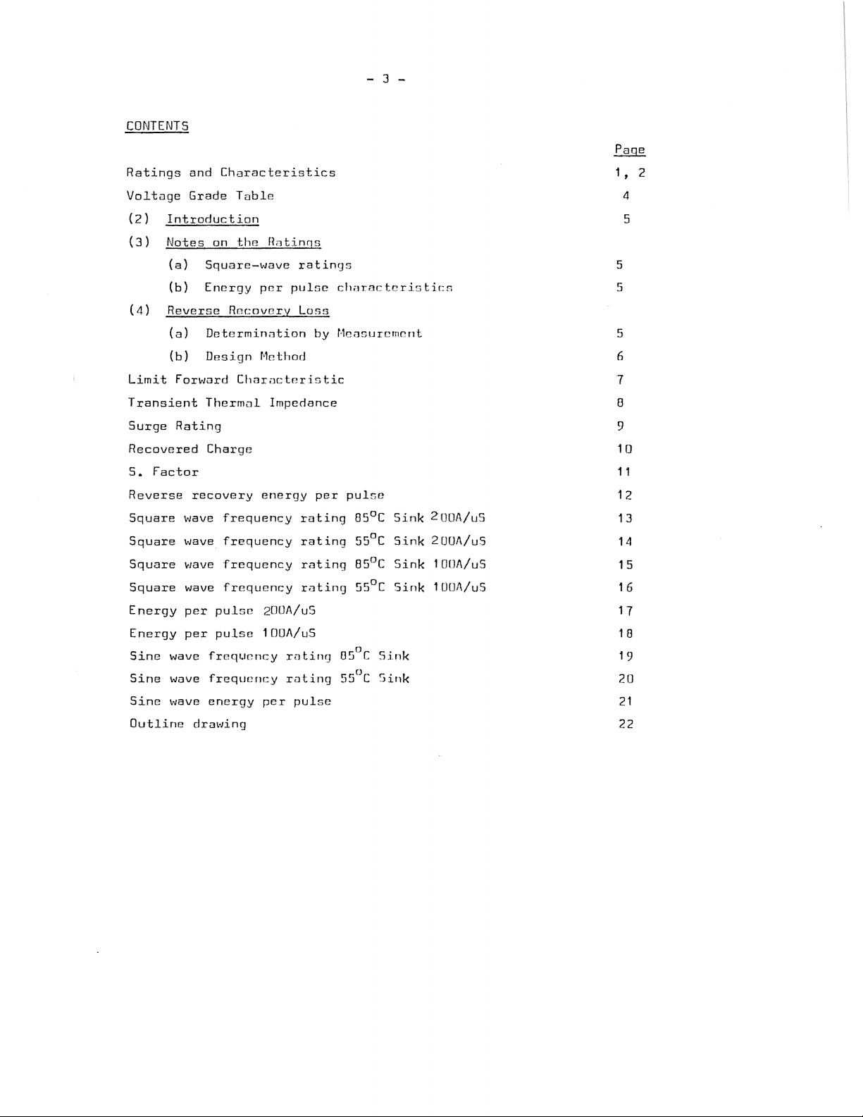
CONTENTS
Ratings
Voltage
(2)
Introduction
(3)
Notes
(a)
(b)
(4)
Reverse
(a)
(b)
Limit
Forward
Transient
Surge
Rating
Recovered
S.
Factor
Reverse
Square
Square
Square
Square
Energy
Energy
Sine
Sine
Sine
wave
wave
vJave
wave
per
per
wave
wave
wave
Outline
and
Characteristics
Grade
on
Table
the
Square-wave
Energy
Recovery
Determinotion
Design
Characteristic
Thermol
CharC]D
recovery
frequency
frequency
Frequency
frequency
pulse
pulse
frequency
frequency
energy
drill"ing
Rntings
ratings
per
pUlf.18
loss
Method
Impedance
energy
rating
rating
rating
roting
2[]
(J
1\/
uS
100A/uS
Totinq
rating
per
pulse
- 3 -
ch;lraci:eri.:3t:ir:!l
by
Measurement
pc.r
pulse
Sink
85°C
55°C
Sink
8SoC
Sink
55DC
Sink
osoe
Sink
55()C
Sink
200A/uS
2
DUA/
uS
1
[l!JI\/
uS
1 (lOA/uS
Page
1 ,
4
5
5
5
5
6
7
8
9
10
11
12
13
14
15
1 6
17
1 8
19
2fJ
21
22
2
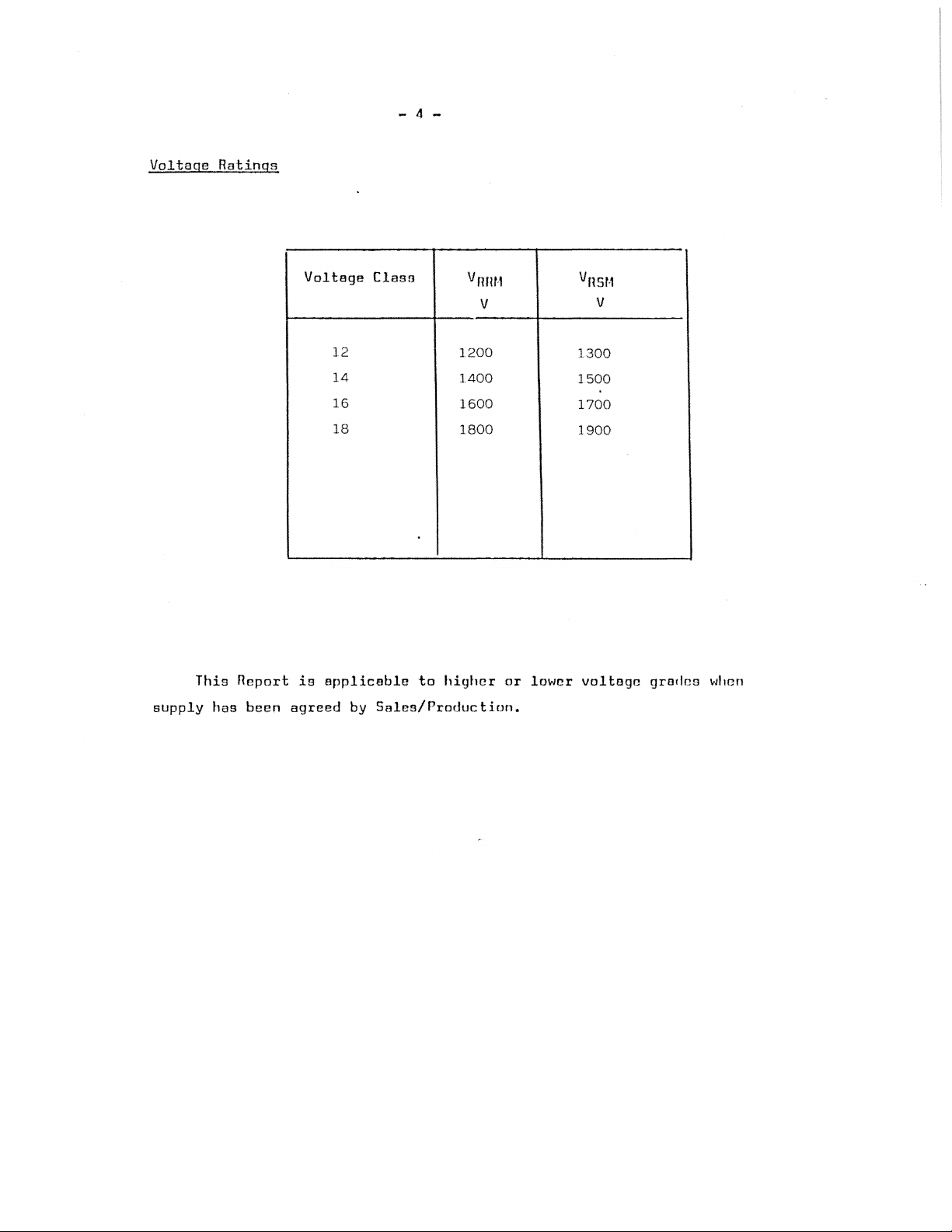
- 4 -
Voltage
Ratings
Voltaga
12
14
16
18
ClasG
Vum·,
V
1200
1400
1600
1800
"nSf-1
V
1300
1500
1700
1900
.
supply
This
has
Ileport
been
is
applicable
agreed
to
higher
by
Sales/Production.
or
lower
voltage
grades
when
2.0
INTRODUCTION
The
diode
all
diffused
characteristics
3.0
NOTES
(a)
Square
silicon
ON
series
with
THE
comprises
slices.
good
RATINGS
wave
ratings
"S"
- 5 -
fast
All
these
factors.
recovery
diodes
cold-weld
have
controlled
capsules
with
reverse
recovery
forward
(b)
obtained
4.0
On
voltage,
The
following
reverse
(a)
(see
reverse
waveform
evaluated
These
current
Energv
These
for
Let:
Then W
and T
REVERSE
RECOVERY
account
no
allo~lance
procedure
recovery
Determination
from waveforms
Note
recovery
be
ratings
ger
curves
conditions
Ep
be
width,
=
AV
=
S1NK
of
the
loss.
1)
and
A
joules
from:
ere
given
of
200
and
pulse
characteristics
enable
rapid
not
the
Energy
in
joules.
Ep x f.
TJ{MAX)
- W
LOSS
number
for
is
of
reverse
recommended
by Measurement
of
recovery
reverse
loss
waveform must be.
per
for
lOOA/uS
covered
per
AV
circuit
recovery
voltage
pulos.
leading
estimation
by
pulse
for a given
Rth
variables
loss
for
use
current
present
A
oe\<1
edge
linear
of
device
the
frequency
affecting
has
been
where
obtained
during
constructed.
heat
sink
rates
dissipation
ratings.
current
made
it
is
necessary
from a
recovery,
Let
temperature
of
and
reverse
in
these
high
frequency
an
instantaneous
the
area
can
rise
to
pUlse
recovery
to
then
of
be
ratings.
include
shunt
under
be
this
T
SINK
(new)
t =
A =
f =
The
where r
duration
Area
rated
total
=
t
of
under
reverse
frequency
dissipation
1.64
reverse
W(TDT) = W(original)
x
10-4~
at
is
+ Axf
recovery
loss
the
original
now
loss
v/aveform
given
heat
by
per
per
pulse
pulse
sink
+
in
microseconds
in
joules
temperature
(W.S.)
NOTE
- 6 -
1
REVERSE
This
recovery
that:
(a)
(bl
(c)
(bl
Desigo
In
conditions,
from
curves
Let
page
12)
RECOVERY
device
LOSS
has a low
current.
a.c.
coupled
affected
The
measuring
100
screen
Idithout
f·1easurcment
out
with
series
connected
Method
circumstances
or
for
on
page
E be
the
BY
MEASUREMENT
I:lhen
measuring
devices
by
prior
oscilloscope
heights
ave.rlood.
of
an
appropriate
where
design
value
of
reverse
pBssage
-
reverse
across
I
it
purposes,
eoergy
recovered
the
su~h
as
of
to
~opc
recovr:ry
snubber
diode
is
not
per
churge
current
high
has
with
possible
the
reverse
charge
care
transformers
amplitude
adequate
the
volt;J(Je
of
O.luF
anode
to
additional
cycle
must
dynamic
initial
Itwveform
cathode.
to
measure
losses
and
be
forward
and
in
peak
reverse
taken
BrB
to
not
ensure
current.
range -typically
forward
5 ohms
voltage
may
joules
should
be
(curves
current
be
in
ar,d
estimated
carried
current
on
Let f be
Then
Where T
original
the
operiJ-ting
T (nelr/) ( ) E R f
is
SINK
SINK
the
nelr!
heat
= TSINK
is
sink
frequency
original
the
required
temperature
in
Hz
- x
mnximulll
given
th
heat
vJith
x .
thr.
sink
frcq'ueocy
temperature
ratings.
and
T
SINK
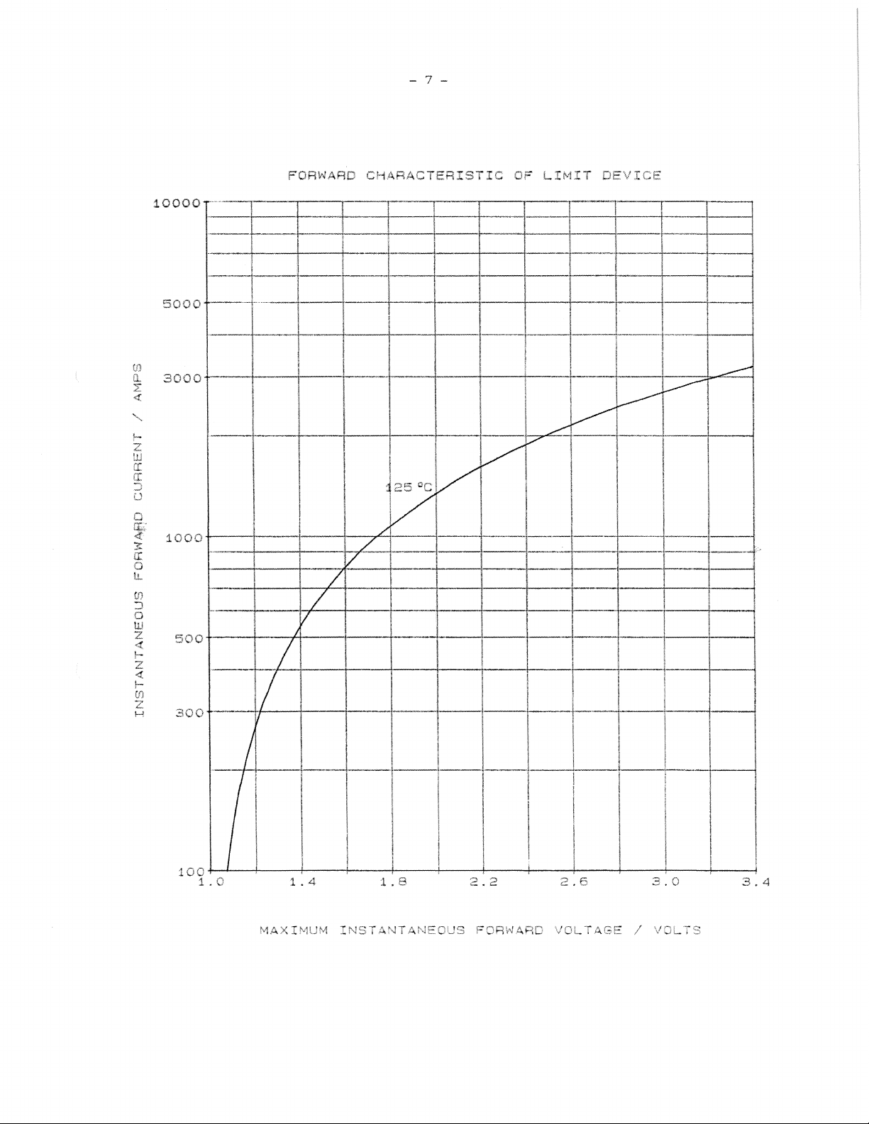
- 7 -
ID
!l
1':
«
"-
!-
Z
W
cr
a::
...,
-'
U
0
:t
5:
ir
0
IJ..
en
:J
0
ill
Z
<!.
I-
Z
<!.
I-
ID
Z
H
1.0000
5000
3000
1000
500
300
.",h."
FORWARD
/
/
I
V
/
CHARACTERISTIC
250C/
V
/
/
V
/
Lt
/
OF
I
LIMIT
~
/'
~
,
DEVICE
~
--
----
--'
100
1.0
I
1.4
MAXIMUM
1.8
INSTANTANEOUS
I
2.2 2.6
FORWARD
VOLTAGE I VOLTS
3.0
t
3.4