

Soft Recovery Diode
Types M0371YH350 to M0371YH450
The data sheet
on
the subsequent pages of this document is a scanned copy of existing
data for this product.
(Rating Report 93NR4
Issue
This data reflects the old part number for this product which
number must
NOT be used for ordering purposes - please use the ordering particulars
detailed below.
The limitations of this data are as follows:
Device no longer available for grades
Please use the following link to view
an
30
to
34
(3000V to 3400V V
up
to
date outline drawing for this device
Outline W3
Where any information
on
the product matrix page differs from that
the product matrix must be considered correct
An electronic data sheet for this product
For further information
on
this product, please contact your local ASM or distributor.
is
presently
Alternatively, please contact Westcode as detailed below.
1)
is:
SM30-45HXC164. This part
)
RRM
in
the following data,
in
preparation.
M0371
Fixed Type Code
Typical Order Code:
IXYS
Semiconductor
Edisonstra[\e
D-68623 Lampertheim
Tel:
+496206
Fax: +49 6206 503-627
E-mail: marcom@ixys.de
IXYS
Corporation
3540 Bassett Street
Santa Clara
Tel:
Fax:
E-mail: sales@ixys.net
The
permission
In
the interest
Devices with a suffix
and limits contained in this report
CA 95054 USA
+1
(408) 982 0700
+1
(408) 496 0670
information contained herein is confidential and is protected by
of
and in the
of
product improvement,
GmbH
15
503-0
manner
permitted by the proprietors West code Semiconductors Ltd,
code
(2-letter, 3-Jet!er or letter/digitl!etter combination) added to
Fixed
~Jl0371YH400,
Westcode
reserves the right to change specifications
Ordering Particulars
YH
Voltage code
Outline Code
26mm clamp height,
An
[iIXYS
Company
www.westcode.com
www.ixys.com
Copyright
The information may not be used or disclosed except
their
at
any time 'Nithout prior notice
generic code are not necessarily subject
V
RRM
••
/100
35-45
4000V
V
RRM
wHh
to
0
Fixed Code
Westcode
Langley Park Way, Langley Park,
Chippenham, Wiltshire, SN15 1GE.
E-mail: WSLsalesri1Jwestcode.com
Westcode
E-mail:
the written
the condItions
Semiconductors
Tel: +44 (0)1249444524
Fax: +44
Long Beach CA
WSI
(0) 1249 659448
Semiconductors
3270 Cherry Avenue
Tel:
+1
Fax:
+1
sales@westcodecom
© West code Semiconductors Ltd
Ltd
Inc
90807
(562) 595 6971
(562) 595 8182
USA
II
Page
Issue
QUALITY AND EVALUATION LABORATORY
1
II
Rating
Origin:
Written
30
voltage
capsule.
Ratings
Voltage
V
RSM
V
RRM
IP(rms) T
Ip
Report
Q.E.L.
by:
mm
gate
Grades
Single
Double
Single
HS
T
HS
No: 93NR4
(0\
M.J.
Silicon
turn-off
= 25°C
= 25°C
Diode
.--=r:
~.fi~~'
Perry
with
phase:
Side
Cooled
Side
Cooled
low
thyristor
50
Hz,
Double
Capsule
Checked:
recovered
180°
T
HS
THS
Type:
applications;
half
= 55°C,
= 100nC
side
cooled
Date:
Pages:
SM30-4SHXC164
M
gJ.....er
charge
sinewave;
10~C
for
16th
snubber
housed
(Converter
25
in
June,
duties
a
high
30-45
3100-4600V
3000-4500V
Ratings)
364A;
147A
678A
597A
1993
in
voltage
high
239A
IpSM : t =
t
I2t
I2t
2
r
T
HS
T
stg
t
t
t =
t
Operating
:
Non-operating
10ms
10ms
10ms;
10ms;
3ms;
Range
half
sinewave;
half
sinewave;
(initial)
TJ
TJ (initial)
(initial)
TJ
V
RM
TJ (initial)
= O. 6V
TJ (initial)
lSO°C;
lsoaC;
RRM(MAX)
lSO°C;
V
V
VRM
RM
RM
<
<
'"
150°C
IS0°C
O. 6V
10V
10V
RRM
(MAX)
4900A
5400A
x
X
to
to
103A2S
103A2S
+150°C
+150°C
120
146
110 X 103A2S
-40
-40
Characteristics
- 2 -
R.R.
R.R.
Page
No.
Issue
Issue
93NR4
1
1
(Maximum
rg
A T
B T
C
D T
A
B
C
D
V
Rth(J-HS)
IRRM
Vfr
pM
J
J
TJ 25°C
J
at
:
:
values
25°C
25°C
=
rpM
Double
Single
at
at
dI/dt
25°C
unless
63SA
=
side
side
VRRM(MAX)
lOOOA/ps
cooled
cooled
otherwise
stated)
1.0SV
1.6Smohms
0.171044306
0.203488535
7.4078071E-4
1.
50068853E-2
0.125659408
0.109853554
7.39508871E-4
3.11942547E-2
2.10V
0.10
K/W
0.20
K/W
SOmA
370V
Reverse
QRR
(total
QRA
(50%
trr
(50%
IRM
Mounting
Outline
JEDEC
NOTE:
recovery
area)
chord)
chord)
Force
Drawing
Outline
All
characteristics
unless
No.
stated
at
rpM = 1000A;
diR/dt
otherwise.
=
are
tp = sOOps:
200A/uS;
at
TVJ
V
RM
TJmax
=
SOV
operating
1s60pC
640pC
3.3ps
400A
330-550
100A317
Kgf
CONTENTS
Ratings
and
characteristics
- 3 -
R.R.
R.R.
Page
No.
Issue
Issue
93NR4
1
1
Page
1,
2
Voltage
2.
Introduction
3.
Notes
(a)
(b)
(c)
(d)
4.
Reverse
(a)
(b)
Limit
forward
Transient
Surge
rating
Forward
Recovered
Reverse
grade
on
table
the
Square
Energy
ABCD
Reverse
Recovery
Determination
Determination
characteristic
thermal
recovery
charge
recovery
Ratings
wave
per
constants
Recovery
impedance
voltage
current
ratings
pulse
Loss
characteristics
Ratings
by
Measurement
without
Measurement
10
11
12,
14
4
5
5
5
5
5
6
6
8
9
13
Reverse
Square
Square
Square
Square
Energy
Energy
Sine
Sine
Sine
Outline
wave
wave
wave
wave
per
per
wave
wave
wave
recovery
frequency
frequency
frequency
frequency
pulse
pulse
frequency
frequency
energy
drawing
energy
100A/jiS
SOOA/!1S
rating
rating
per
pulse
per
rating
rating
rating
rating
pulse
55°C
55°C
85°C
85°C
55°C
85°C
Sink
Sink
Sink
Sink
Sink
Sink
100A/jiS
SOOA/jiS
lOOA/!1
500A/!1
15
16
17
S
S
18
19
20
21
22
23
24
25
- 4 -
R.R.
No. 93NR4
R.R.
Issue
Page
Issue
1
1
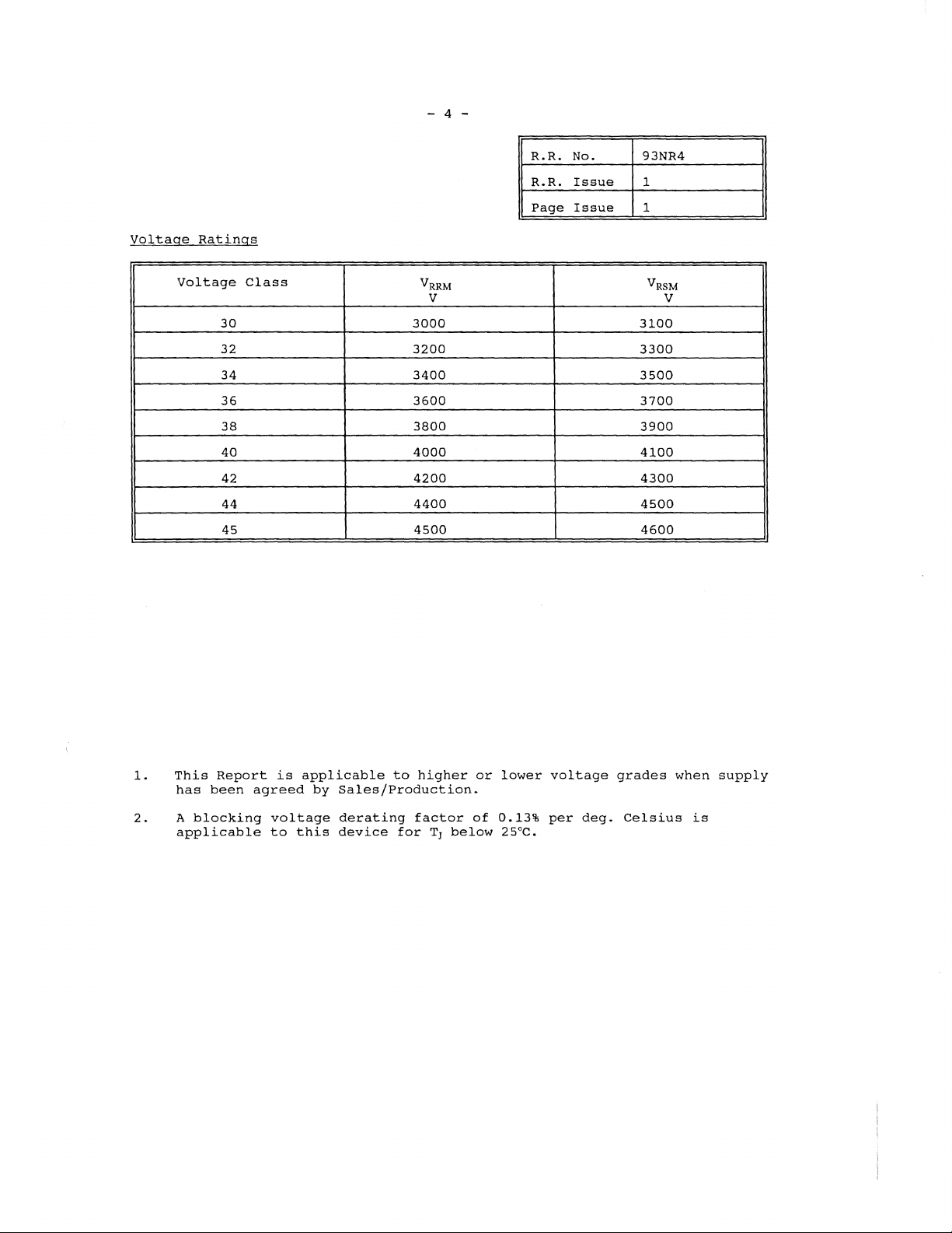
Voltage
Ratings
Voltage
30
32
34
36
38
40
42
44
45
Class
V
RRM
V
RSM
V
3000
3200
3400
3600
3800
4000
4200
4400
3100
3300
3500
3700
3900
4100
4300
4500
4500 4600
V
1.
2.
This
Report
has
been
A
blocking
applicable
is
agreed
voltage
to
applicable
by
Sales/Production.
derating
this
device
to
for
higher
factor
TJ below
or
of
lower
0.13%
25°C.
voltage
per
deg.
grades
Celsius
when
is
supply
- 5 -
R.R.
No. 93NR4
R.R.
Issue
Issue
Page
1
1
2.0
diffused
INTRODUCTION
The
diode
silicon
characteristics.
SCR
snubber
3.0
NOTES
(a)
(b)
(c)
series
slices.
These
networks.
ON
THE
RATINGS
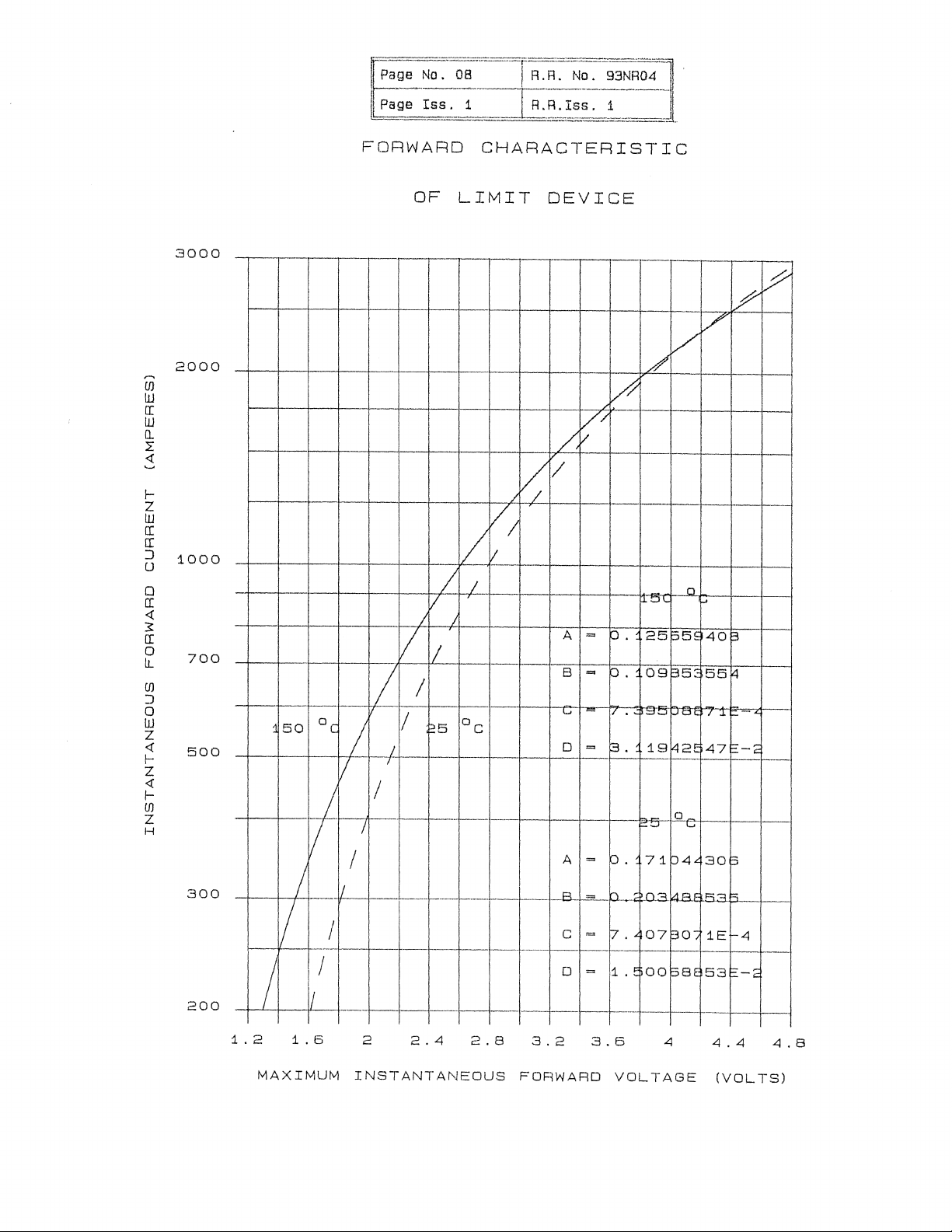
Sguare
These
forward
Energy
These
obtained
Let:
Then
TSlNK = TJ(MAX)
ABCD
These
wave
ratings
current
per
curves
for
Ep
be
in
joules,
WAY = Ep
Constants
constants
characteristic
for
the
forward
comprises
diodes
ratings
are
pulse
enable
conditions
the
Energy
x f
-
(Ep
on
All
these
are
particularly
given
of
for
100A/~S
characteristics
rapid
not
per
and f be
x f x
(applicable
fast
page
8)
characteristic
recovery
diodes
have
leading
and
500A/~S.
estimation
covered
pulse
~hJ-HS)
the
only
are
for a given
repetition
over
the
given
capsule
controlled
suitable
edge
linear
of
device
by
the
rate.
current
co-efficients
below:
devices
for
use
rates
dissipation
frequency
current
range
of
reverse
in
ratings.
and
of
the
with
recovery
G.T.O.
of
rise
to
pulse
V
F
expression
all
and
of
be
width
(d)
V
= A + B
F
current.
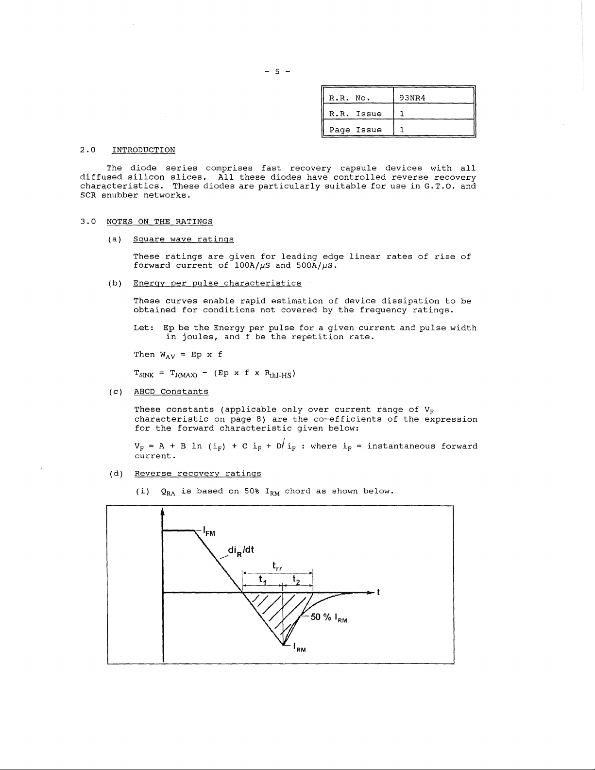
Reverse
(i)
QRA
ln
recovery
is
based
(iF)
+ C
ratings
on
50%
iF
+
IRM
DJ
iF : where
chord
as
iF = instantaneous
shown
below.
forward
- 6 -
R.R.
R.R.
Page
No.
Issue
Issue
93NR4
1
1
4.0
include
(ii)
(iii)
Reverse
The
Recovery
following
reverse
(a)
Determination
From
shunt
(see
instantaneous
the
area
temperature
TSINK
where
t
A
f
(new) = TSINK
r
t
duration
Area
Rated
is
QRR
Le.
K
factor
procedure
recovery
waveforms
Note
reverse
under
can
3.30E-6
of
under
frequency
based
QRR
Loss
by
1)
this
then
reverse
reverse
on
=
tdt2
is
loss.
measurement
of
recovery
and
reverse
recovery
waveform
be
evaluated
(or
ig
inal
x t
recovery
loss
at
the
a
1S0uS
integration
1S0uS
iRR
J
t 0
recommended
current
voltage
loss
be A joules
from:
-
A(
)
Tt
( t
(K/W)
loss
waveform
original
dt
for
obtained
present
waveform
per
6
x
10
per
per
pulse
sink
temperature.
use
+
pulse
time
where
from a high
during
must
pulse.
R
thJ-HS
in
in
it
is
recovery,
be
constructed.
A
new
X f
microseconds.
joules
(W.S.)
necessary
frequency
sink
to
an
Let
The
total
W(TOT)
(b)
current
A
Let E be
p1S)
Let f be
then
where
TSINK
==
W(oTiginal) + A x f
Determination
In
circumstances
conditions,
in
joules
.
TSINK new
TSINK new
original
the
the
ratings.
A
suitable
restrict
(VRM)
of
the
0.67
If a different
Grade,
of
the
the
maximum
dissipation
may
be
value
operating
==
is
is
the
R-C
snubber
transient
of
grade
reverse
value
without
estimated
of
TSINK
the
heat
the
loss
is
where
or
for
energy
frequency
original
required
sink
network
reverse
maximum
is
being
may
obtained
now
given
Measurement
it
is
design
from
per
- (E X
maximum
temperature
grade.
used
be
from
by
not
possible
purposes,
curves
reverse
in
Hz
Rth
X
f)
heat
is
connected
voltage
or
waveform
V
RM
approximated
the
curves
on
cycle
given
is
to
the
page
measure
additional
15.
in
sink
temperature
with
across
to a peak
lower
by a pro
provided.
joules
the
the
than
rata
voltage
losses
(curves
frequency
diode
value
0.67
adjustment
and
on
and
to
of
NOTE
- 7 -
No.
R.R.
R.R.
Page
Issue
Issue
93NR4
1
1
1
Reverse
current.
Recovery
This
(a)
(b)
(c)
anode
Loss
device
When
a.c.
by
A
input
has a low
measuring
coupled
prior
suitable,
of
internal
current
signal.
Measurement
an
appropriate
to
cathode.
by
Measurement
the
devices
passage
polarised,
the
measuring
amplifiers
of
reverse
snubber
reverse
charge
of
high
by
recovered
care
such
as
amplitude
clipping
oscilloscope
the
recovery
of
O.5~F,
must
current
circuit
relatively
waveform
2.2ohms
charge
be
taken
transformers
forward
to
avoid
high
and
peak
current.
must
amplitude
should
connected
reverse
to
ensure
are
be
connected
overloading
be
carried
across
recovery
that:
not
affected
the
forward
out
to
the
with
diode
,....,
(f}
W
0:
W
Q.
L
<t
f--
Z
W
0:
0:
:J
U
0
0:
<t
~
0:
0
lL
(f}
:J
0
W
Z
<t
f-Z
<t
!-
(f}
Z
H
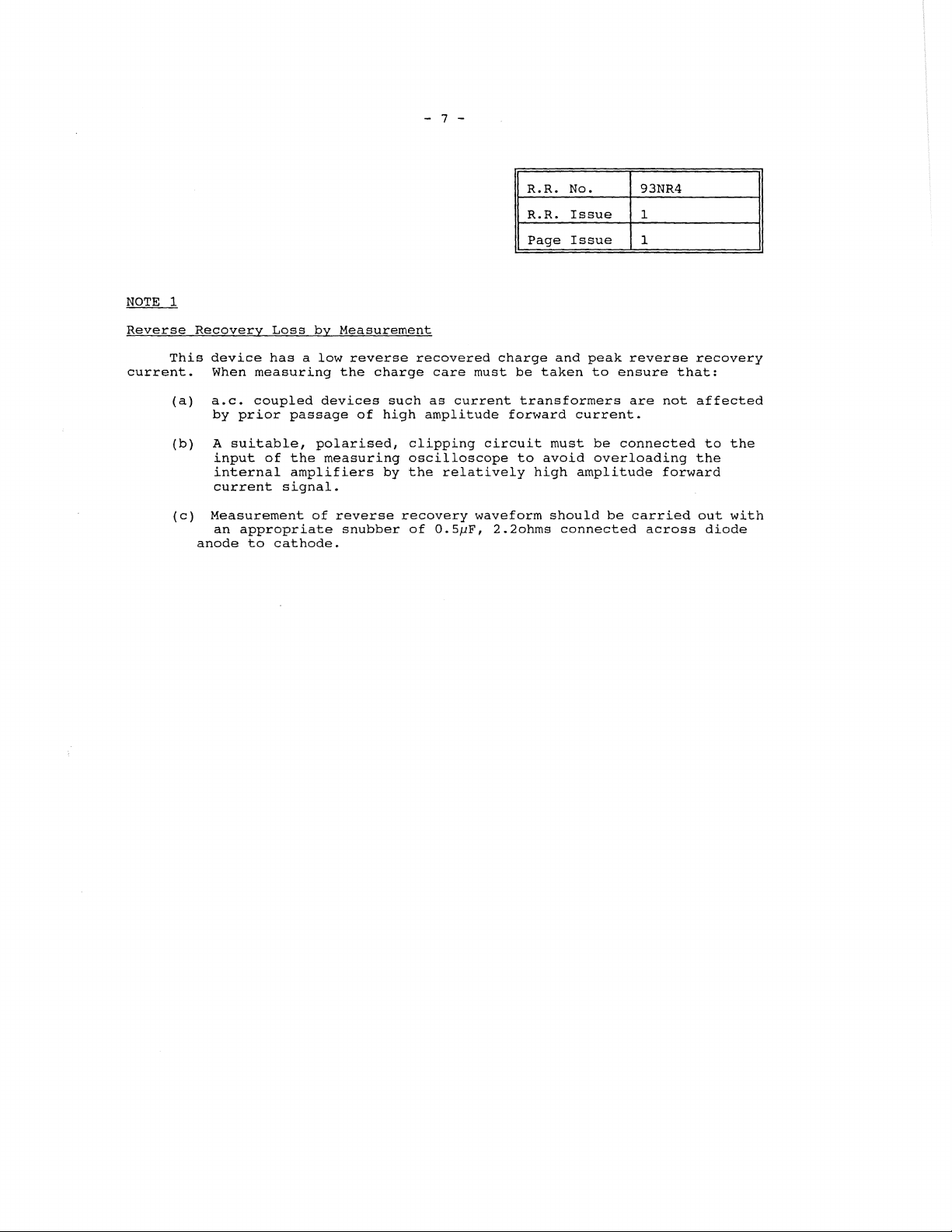
3000
2000
1000
700
500
50
DC
/
FORWARD
/
L
V
/
I
I
/
/
V
/
/
I
OF
V
L /
II
/
~5
CHARACTERISTIC
LIMIT
DEVICE
/,
/
~
L
VI
II
1/
/
L
A
8
....
°c
D
A
V/
V
=
=
=0
==
V
p.
p.
13·
p.
V
./
• , ....
1\
..
25
p5~
09
13
~:::IW
1-''-'
19
142E
F''-'
71
P4~
~
~
V
D
r-
403
5
::
55/4
,
oJ.
t-
f,':-;:
47
0
w
30
IS
300
200
/
1.2
MAXIMUM
/
1.6
/
II
II
/
/
2
INSTANTANEOUS
2.4 2.8
p.
==
c
==
D
==
3.2
FORWARD
3.6
h
17.
1 .1:
VOLTAGE
.0.3.
07
00
I.1P.F
F30"
SSE
4
F;
kFi:::l
1E
t-4
E-;:
53
4.4 4.8
(VOLTS)
 Loading...