

Westcode Semiconductors K2960T#450, K2960T#520 Data Sheet
Date:- 9 Oct, 2003
WESTCODE
An
Absolute Maximum Ratings
V
DRM
V
DSM
V
RRM
V
RSM
I
T(AV)M
I
T(AV)M
I
T(AV)M
I
T(RMS)
I
T(d.c.)
I
TSM
I
TSM2
I2tI
I2t
(di/dt)
V
RGM
P
G(AV)
P
GM
T
j op
T
stg
IXYS
Company
Provisional Data
Medium Voltage Thyristor
Types K2960T#450 to K2960T#520
Old Type No.: P1263DH45-52
VOLTAGE RATINGS
Repetitive peak off-state voltage, (note 1) 4500-5200 V
Non-repetitive peak off-state voltage, (note 1) 4500-5200 V
Repetitive peak reverse voltage, (note 1) 4500-5200 V
Non-repetitive peak reverse voltage, (note 1) 4600-5300 V
OTHER RATINGS
Maximum average on-state current, T
Maximum average on-state current. T
Maximum average on-state current. T
Nominal RMS on-state current, T
D.C. on-state current, T
Peak non-repetitive surge tp=10ms, Vrm=0.6V
Peak non-repetitive surge tp=10ms, V
2
t capacity for fusing tp=10ms, Vrm=0.6V
2
t capacity for fusing tp=10ms, V
I
Critical rate of rise of on-state current (continuous, 50Hz), (Note 6) 150 A/µs
Critical rate of rise of on-state current (repetitive, 50Hz, 60s), (Note 6) 300 A/µs
cr
Critical rate of rise of on-state current (non-repetitive), (Note 6) 600 A/µs
Peak reverse gate voltage 5 V
Mean forward gate power 5 W
Peak forward gate power 50 W
Operating temperature range -40 to +125 °C
Storage temperature range -40 to +150 °C
=25°C, (note 4) 5095 A
sink
rm
=55°C, (note 2) 2960 A
sink
=85°C, (note 2) 2044 A
sink
=85°C, (note 3) 1248 A
sink
=25°C, (note 2) 5825 A
sink
, (note 5) 32.5 kA
RRM
≤
10V, (note 5)
rm
, (note 5)
RRM
≤
10V, (note 5) 6.48×10
Data Sheet Issue:- 2
MAXIMUM
LIMITS
MAXIMUM
LIMITS
36 kA
5.28×10
6
6
UNITS
UNITS
A2s
A2s
Notes:-
1)
De-rating factor of 0.13% per °C is applicable for Tj below 25°C.
2)
Double side cooled, single phase; 50Hz, 180° half-sinewave.
3)
Single side cooled, single phase; 50Hz, 180° half-sinewave.
4)
Double side cooled.
5)
Half-sinewave, 125°C Tj initial.
6)
VD=67% V
Provisional Data Sheet. Types K2960T#450 to K2960T#520 Issue 2 Page 1 of 11 October, 2003
, IFG=2A, t
DRM
≤
0.5µs, T
r
case
=125°C.
WESTCODE
WESTCODE
WESTCODEWESTCODE
An IXYS Company
Characteristics
Medium Voltage Thyristor Types K2960T#450 to K2960T#520
PARAMETER MIN. TYP. MAX. TEST CONDITIONS
V
TM
V
TM
V
T0
r
T
(dv/dt)crCritical rate of rise of off-state voltage 1000 - - VD=80% V
I
DRM
I
RRM
V
tr
V
GT
I
GT
V
GD
I
H
t
gd
t
gt
Q
rr
Q
ra
I
rm
t
rr
t
q
R
thJK
Maximum peak on-state voltage - - 2.1 ITM=4000A V
Maximum peak on-state voltage - - 3.15 ITM=8880A V
Threshold voltage - - 1.229 V
Slope resistance - - 0.212
Peak off-state current - - 150 Rated V
Peak reverse current - - 150 Rated V
On-state recovery voltage - 18 - IT=2×I
Gate trigger voltage - - 3.0 V
T
Gate trigger current - - 600
Gate non-trigger voltage - - 0.25 Rated V
DRM
RRM
T(AV)M
=25°C VD=10V, IT=3A
j
DRM
Holding current - - 1000 Tj=25°C mA
Gate-controlled turn-on delay time 1.0 2.0 µs
Turn-on time - 3.5 5.0
=60% V
V
D
I
=2A, tr=0.5µs, Tj=25°C
FG
Recovered charge - 17000 - µC
Recovered charge, 50% Chord - 11000 12000 µC
Reverse recovery current - 340 - A
I
=4000A, tp=2000µs, di/dt=10A/µs,
TM
V
=100V
r
Reverse recovery time - 65 -
ITM=4000A, tp=2000µs, di/dt=10A/µs,
V
=100V, Vdr=80%V
r
ITM=4000A, tp=2000µs, di/dt=10A/µs,
V
=100V, Vdr=80%V
r
Turn-off time
Thermal resistance, junction to heatsink
- 800 -
- 1600 -
- - 0.0085 Double side cooled K/W
- - 0.017 Single side cooled K/W
(Note 1)
, linear ramp, gate o/c
DRM
, tp=10ms, T
, IT=2000A, di/dt=10A/µs,
DRM
=25°C V
case
, dVdr/dt=20V/µs
DRM
, dVdr/dt=200V/µs
DRM
UNITS
m
V/µs
mA
mA
mA
V
µs
µs
µs
F Mounting force 63 - 77 kN
- 1.23 - Outlines TC & TT
W
Weight
t
kg
- 1.70 - Outlines TD & TV
Ω
Notes:-
Unless otherwise indicated Tj=125°C.
1)
For other clamp forces consult factory.
2)
Notes on rupture rated packages.
This product is available with a non-rupture rated package.
For additional details on these products, please consult factory.
Provisional Data Sheet. Types K2960T#450 to K2960T#520 Issue 2 Page 2 of 11 October, 2003
WESTCODE
WESTCODE
WESTCODEWESTCODE
An IXYS Company
Notes on Ratings and Characteristics
1.0 Voltage Grade Table
Medium Voltage Thyristor Types K2960T#450 to K2960T#520
Voltage Grade
V
DRM VDSM VRRM
V
V
RSM
V
V
V
D
DC V
R
45 4500 4600 2100
46 4600 4700 2120
48 4800 4900 2160
50 5000 5100 2200
52 5200 5300 2240
2.0 Extension of Voltage Grades This report is applicable to other voltage grades when supply has been agreed by Sales/Production.
3.0 De-rating Factor
A blocking voltage de-rating factor of 0.13%/°C is applicable to this device for Tj below 25°C.
4.0 Repetitive dv/dt
Standard dv/dt is 1000V/µs.
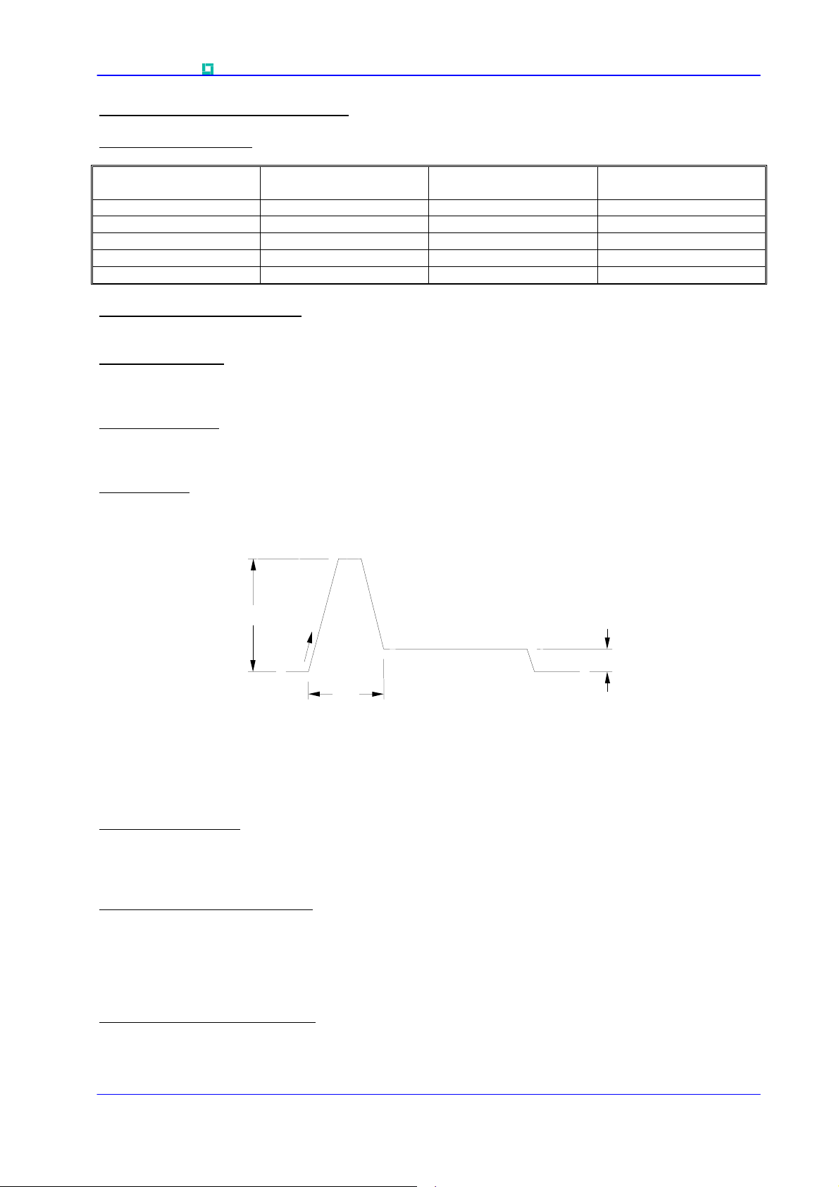
5.0 Gate Drive
The nominal requirement for a typical gate drive is illustrated below. An open circuit voltage of at least 30V
is assumed. This gate drive must be applied when using the full di/dt capability of the device.
I
GM
4A/µs
I
G
t
p1
The magnitude of IGM should be between five and ten times IGT, which is shown on page 2. Its duration
) should be 20µs or sufficient to allow the anode current to reach ten times IL, whichever is greater.
(t
p1
Otherwise, an increase in pulse current could be needed to supply the necessary charge to trigger. The
‘back-porch’ current I
magnitude in the order of 1.5 times I
should remain flowing for the same duration as the anode current and have a
G
.
GT
6.0 Frequency Ratings
The curves illustrated in figures 17 & 18 are for guidance only and are superseded by the maximum
ratings shown on page 1. For operation above line frequency, please consult the factory for assistance.
7.0 Rate of rise of on-state current
The maximum un-primed rate of rise of on-state current must not exceed 1000A/µs at any time during
turn-on on a non-repetitive basis. For repetitive performance, the on-state rate of rise of current must not
exceed 500A/µs at any time during turn-on. Note that these values of rate of rise of current apply to the
total device current including that from any local snubber network.
8.0 Square wave frequency ratings
These ratings are given for load component rate of rise of on-state current of 50A/µs.
Provisional Data Sheet. Types K2960T#450 to K2960T#520 Issue 2 Page 3 of 11 October, 2003
WESTCODE
p
p
WESTCODE
WESTCODEWESTCODE
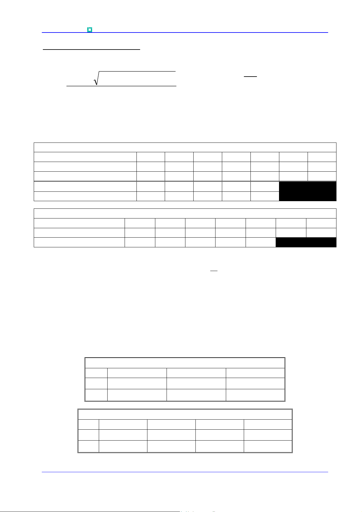
9.0 Computer Modelling Parameters
9.1 Device Dissipation Calculations
I
AV
Where VT0=1.229V, rT=0.212mΩ,
R
= Supplementary thermal impedance, see table below and
th
ff
= Form factor, see table below.
Square wave Double Side Cooled 0.00923 0.00915 0.00907 0.00899 0.00884 0.00864 0.0085
Square wave Single Side Cooled 0.01801 0.01792 0.01783 0.01775 0.01760 0.01739 0.0170
Sine wave Double Side Cooled 0.00917 0.00906 0.00898 0.00890 0.00867
Sine wave Single Side Cooled 0.01794 0.01782 0.01773 0.01765 0.01742
An IXYS Company
2
4
=
00
2
Conduction Angle 30° 60° 90° 120° 180° 270° d.c.
2
⋅⋅⋅++−
WrffVV
AVTTT
2
⋅⋅
rff
T
Supplementary Thermal Impedance
Medium Voltage Thyristor Types K2960T#450 to K2960T#520
∆
T
=
W
AV
and:
R
th
max
−=∆
TTT
Hsj
Form Factors
Conduction Angle 30° 60° 90° 120° 180° 270° d.c.
Square wave 3.464 2.449 2 1.732 1.414 1.149 1
Sine wave 3.98 2.778 2.22 1.879 1.57
9.2 D.C. Thermal Impedance Calculation
−
=
np
∑
=
p
1
Where
The coefficients for this device are shown in the tables below:
p = 1
t = Duration of heating pulse in seconds.
r
= Thermal resistance at time t.
t
= Amplitude of pth term.
r
τ
= Time Constant of rth term.
to
n, n
is the number of terms in the series and:
D.C. Double Side Cooled
Term
r
p
τ
p
123
4.934536×10
0.8203239 0.1170407 0.0170874
-3
1
pt
2.693673×10
t
τ
p
−⋅=
err
-3
8.295909×10
-4
D.C. Single Side Cooled
Term
r
p
τ
p
Provisional Data Sheet. Types K2960T#450 to K2960T#520 Issue 2 Page 4 of 11 October, 2003
1234
0.01011545 3.424005×10
5.990464 1.10841 0.140561 0.02103968
-3
2.491583×10
-3
1.174174×10
-3
 Loading...