

E C E
ICON UCTORS
Technical
Publication
DF
76
iSSUE 2
L. May, 1989
Fast
Recovery
Stud-Base
75 amperes average: up
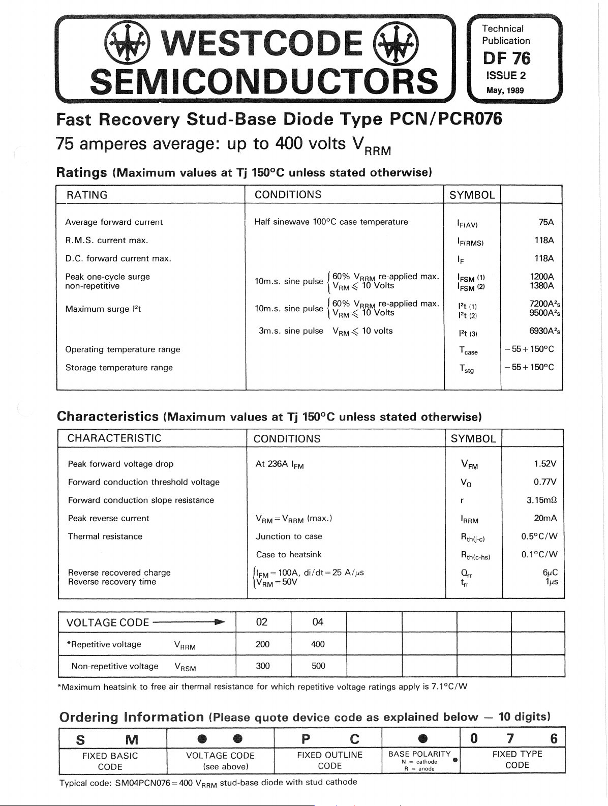
Ratings
RATING
Average
R.M.S.
D.C.
Peak one-cycle surge
non-repetitive
Maximum
Operating temperature range
Storage temperature range
(Maximum
forward
current max.
forward
surge 1
current
current max.
2
t
values
at
Tj
I
Diode
to
400 volts V
150°C
CONDITIONS
Half sinewave
10
10
unless
lOD
. I
m.s.
sme pu
m.s. sine pu
3m.s. sine pulse V
se
. I { 60% V
se
Type
PCN/PCR076
RRM
stated
D
e case temperature
{60%
V
RM
V
RM
RM
otherwise)
V
re-applied max.
RRM
<;
10
Volts
re-applied max.
RRM
<;
10
Volts
<;
10
volts
SYMBOL
IF(AV)
'F(RMS)
IF
i
(1)
FSM
I
(2)
FSM
J2t
(1)
2
1
t
(2)
2
1
t (3)
Tease
T
stg
-55+
-55+
75A
118A
118A
1200A
1380A
7200Ns
9500Ns
6930Ns
0
150
e
0
150
e
Characteristics
CHARACTERISTIC
Peak
forward
Forward
Forward
Peak reverse current
Thermal resistance
Reverse
Reverse recovery
VOL
TAGE
"Repetitive voltage
Non-repetitive voltage
*Maximum
voltage
conduction
conduction
recovered charge
time
CODE
heatsink
to
(Maximum
drop
threshold voltage
slope resistance
V
RRM
V
RSM
free air thermal resistance
values
!lIP
at
Tj
150°C
CONDITIONS
At
236A
IFM
= V
V
RM
Junction
Case
{IFM=
VRM=50V
RRM
to
heatsink
l00A,
(max.)
to
case
di!dt=25
02 04
200 400
300
for
which
500
repetitive voltage ratings apply is
unless
A/I-'s
stated
otherwise)
SYMBOL
V
FM
Va
r
IRRM
Rth(j-c)
Rth(e-hs)
(},.,
tre
7.1°C/W
1.52V
O.77V
3.15mQ
20mA
0.5°C/W
O.l°C/W
61-'C
lf1s
Ordering
S
FIXED
Typical code: SM04PCN076 = 400 V
Information
M
BASIC
CODE
VOL T AGE CODE
(Please
•
(see above)
stud-base diode
RRM
•
quote
device
p
FIXED OUTLINE
CODE
with
stud cathode
code
C
as
explained
BASE POLARITY
N
R =
~:
cathode
•
anode
below
0 1
iii
- 10
digits)
FIXED TYPE
CODE
6
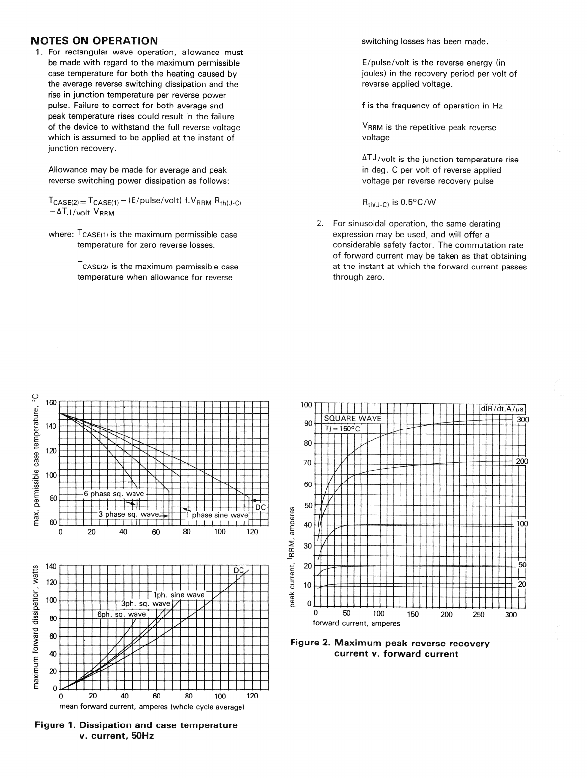
NOTES
1.
ON
OPERATION
For rectangular wave operation, allowance
be
made
with
regard
to
the
maximum
case temperature
the average reverse
rise in
junction
pulse. Failure
peak temperature rises could result in the failure
of
the device
which
is
assumed
junction recovery.
Allowance
switching
reverse
for
both
the
switching
temperature per reverse
to
to
may
correct
withstand
be
for
both
the
to
be applied at the instant
made
for
average and peak
power
dissipation
heating caused
dissipation and the
average and
full reverse voltage
as
must
permissible
by
power
of
follows:
switching losses has been made.
E/pulse/volt
joules) in the recovery period per
reverse applied voltage.
f is the frequency
V
RRM
voltage
il
T J
Ivolt
in deg. C per
voltage per reverse recovery pulse
is
the
reverse energy (in
of
operation in Hz
is
the repetitive peak reverse
is
the
junction
volt
temperature rise
of
reverse applied
volt
of
T CASEI2) = T
-ilTJ/volt
where: T CASEI1) is the maximum permissible case
u
0
160
ai
Z
ro
140
Q;
0.
E
B
120
Q)
rn
ro
u
Q)
100
:0
'ii;
<Il
'E
1--
80
Q;
0.
X
co
60
E
o
~
140
ro
~
120
c
o
ii;
100
0.
.~
80
13
E
co
60
~
E
40
E
:0
E
20
'x
co
E
o
o
mean
CASEll)
-
(E/pulse/volt)
V
RRM
temperature
T CASEI2) is the maximum permissible case
temperature when allowance
~
~~
f"..
for
zero reverse losses.
.......
I"
"
f.
V
RRM
for
"
"
I-
6 phase sq. wave
20
v::~
~~
i"
20
forward
......
1
I
40
1 I I
60
I-r-l
phase sine wave
II
80
3 phase sq. wave_
'rrr
I I I I
I I I I
.II
I. I I I I
3ph. sq. wave
6ph. sq. wave
V
/
Vv
V
/tf/
40 60 80
current, amperes {whole cycle average)
1 ph. sine wave
v:
/:
I/;
/'
~
V
/'
V
RthIJ-C)
reverse
""
I I I J I
100
/'
100
DC,.,-
V
8?=
120
120
RthIJ.C)
is
O.5°C/W
2. For sinusoidal operation, the same derating
expression may be
considerable safety factor. The
of
forward
at the instant at
through
current may
zero.
used, and will
be
which
the
100
ill
Q;
E 40
co
::i
a:
a:
90
80
70
60
50
30
20
SQUARE
Tj ~ 150°C
/
I
II
WAVE
V
/
/
_.
10
o
o
50
forward current, amperes
Figure
2.
Maximum
current
100
peak
v.
forward
150
reverse
current
offer
commutation
taken
as
that
forward
200 250
current passes
recovery
a
rate
obtaining
dlR/dt,A/l's
300
200
100
·r1
."
300
Figure
1.
Dissipation
v.
current.
and
50Hz
case
temperature
100
~SQUARE
50
30
10
5
....
~
0.5
III
-3
0.3
Co
......
>-
~
III
16
0.1
1
rate
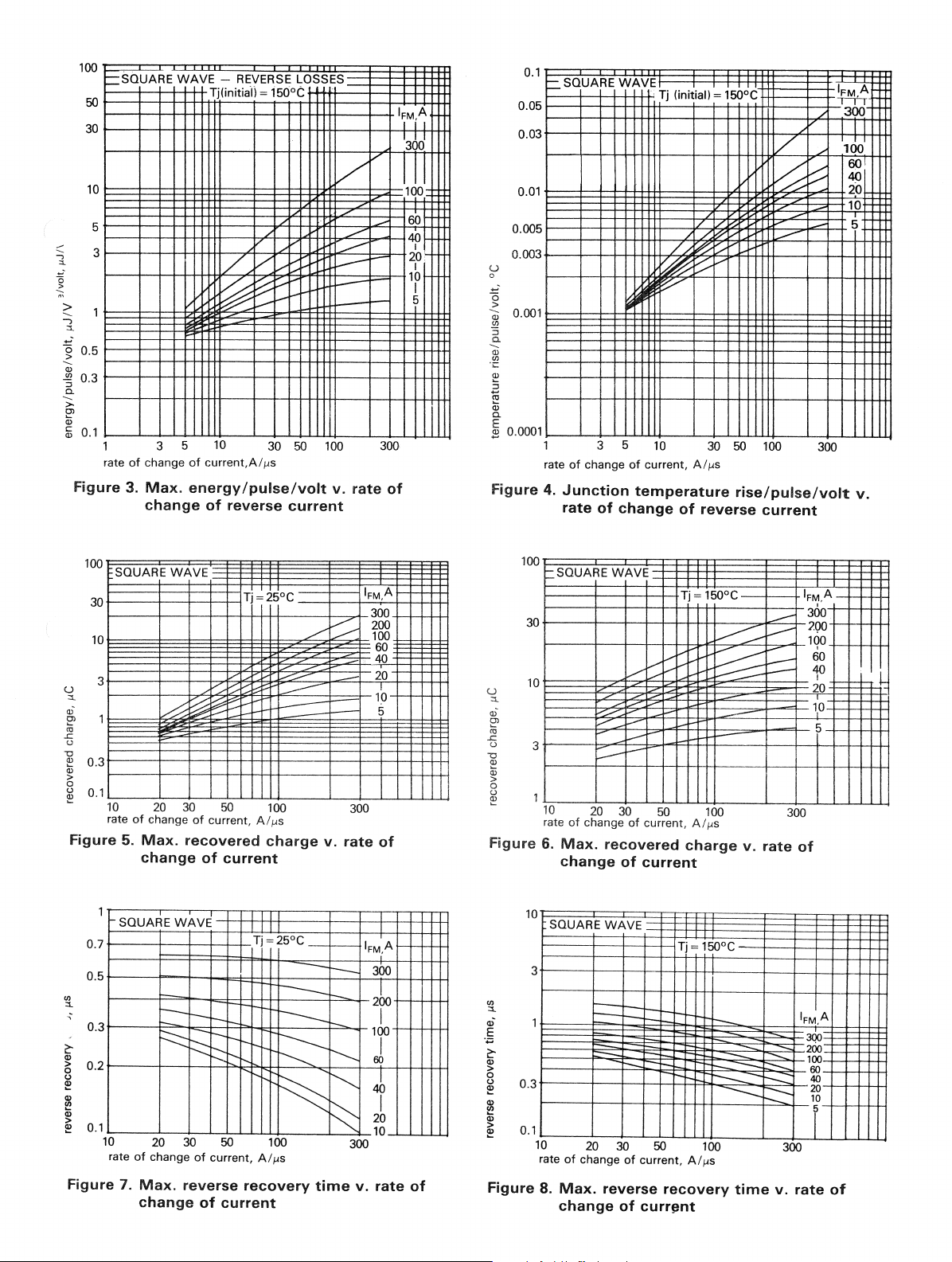
Figure
of
change
3.
Max.
change
WAVE
REVERSE
Tj(initial) 150°C
/
~
3 5
10
of
current,A/l-'s
energy/pulse/volt
of
reverse
V
V-
I-"'"
~
I-
V
30
LOSSES
50
100
current
V~
~
.........-
f--
r
r--
v.
rate
300
of
I A
)M'I
13bd
11LI
60
40
I
20
I
10
I
5
0.1
0.05
0.03
0.01
0.005
0.003
u
°
....
(5
.2:
0.00
3l
::;
Co
......
3l
.;::
III
Z
~
Co
'"
E
$ 0.000
Figure
r- SQUARE WAVE
r-,
1
1
rate
4.
3 5
of
change
Junction
rate
of
change
Tj (initial)
/-
;.e;.
/.
:::::-
~
10
of
current, A/I-'5
temperature
of
reverse
150°C
~c:..
;.,-
,/
30
50
100
rise/pulse/volt
current
k:::
~
~
-
....-
300
IFMA
"TI'T
300
I
II
100
601
40
20
10
5
v.
100
30
10
3
U
:::t..
cO
~
to
.s::
u
-0
~
0,3
~
~
0.1
Figure
0.7
0.5
0.3
0.1
Figure
SQUARE WAVE
d
10
20
rate
of
change
5.
Max.
change
SQUARE
I-
t::::
WAVE
p::::
10
rate
7.
20 30
of
change
Max.
change
v
V
r:
~
~
30
50
of
current, A/I-'s
recovered
of
current
l-
f-.
--
t-
--
:::::
::::
t-b
50
of
current, A/I-'s
reverse
of
current
Tj
25°C
L
......-~
~
------
100
charge
Tj-25°C
-
--t-
---
;:-
~
100
recovery
~
~
300
v.
rate
t::--
r---.
'"
~
300
time
v.
IFM,A
300
200
100
60
40
20
10
5
of
IFM,A
300
2bo
I
100
I
60
-tb
I
20
10
rate
of
Figure
:::t..
'"
cO
,,§
~
~
~
0.3
~
~
Figure
100
I=SQUARE WAVE
30
10
3
1
10
20
rate
of
change
6.
Max.
change
10
SQUARE WAVE
3
0,1
10
rate
of
8.
Max.
change
20
change
.,./
V
~
v-
I-"""
V
r-
I--
30
of
current, A/I-'5
recovered
of
current
r-
-
""-
::-
r--
30
of
current, A/I-'s
reverse
of
currpnt
Tj=
I-"'"
V
50
charge
Tj
-
::-
50
recovery
150°C
:::::::::::
~
r--:::::
t::::::::::
---
::-
r-
=
r-
100
v.
rate
150°C
~
-
........
.::--
c::::::",
r-
r---
~
---
100
time
-
~
v.
300
300
IFM,A
300
7.90
lqO
60
40
I
20
10
5
of
IFM,A
3QO
200
100
60
40
20
01f
rate
r-
of
0.5
~
U
0.1
°
Q)
t.l
C
.gj
0.05
c.
'"
/'
.S
C5
E
Q;
.;:;
0.01
0.001 0.01
time,
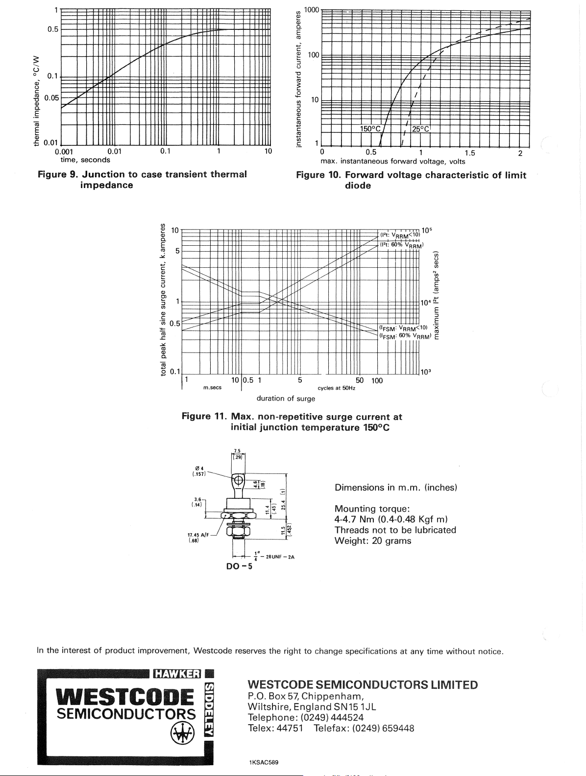
figure
9.
V
V
seconds
Junction
impedance
V
to
case
~
0.1
transient
thermal
10
U)
1000
Q;
'"
c.
E
'"
Ul
::J
o
c
'"
~
c
~
Ul
1
.r:.
o
max. instantaneous forward voltage, volts
Figure
10.
150°C I
Forward
diode
1/
I
0.5
voltage
k-'
/.
I
25°C
characteristic
~i--
1.5
of
-
2
limit
'"
~
10
c.
'"
E
~
5
-'"
c
~
~
::J
t.l
Ol
'"
:;
CIl
c
'"
'iii 0.5
....
C5
.r:
-'"
ro
C.
'"
C5
B
l---
l"-
)---
~
0.1
1
m.secs
Figure
11. Max.
04
(.157)
17.45A/f~
1.68)
-
-
:;><
10
0.5 1 5
duration
non-repetitive
initial
junction
vV'
/
V
--
cycles
of
surge
temperature
(l't:
1I't: 60% VRRM
./
at
50Hz
V
IIFSM:
t----.
--
IIFSM: 60%
50
100
current
V'
surge
150°C
Dimensions
Mounting torque:
4-4.7 Nm
Threads
Weight:
(0.4-0.48 Kgf m)
not
20
grams
5
VRRM<l
VR
10
4
10
01
RMI E
3
10
VRRM<101
at
in
m.m. (inches)
to
be
lubricated
Ul
t.l
Ul
'"
N
CIl
c.
E
ro
~
E
::J
E
'x
co
In the interest
•
_____
of
product
improvement,
1:(W133:;;1
Westcode
ESTCO E
SEMICONDUCT~
reserves the right
II
~
~
to
change specifications at any time
without
WESTCODE SEMICONDUCTORS LIMITED
P.O. Box
Wiltshire,
Telephone: (0249) 444524
Telex: 44751 Telefax: (0249) 659448
1
KSAC589
57,
Chippenham,
England
SN151JL
notice .
 Loading...