

Technical
Publication
@WESTCODE@
DF
ISSUE 2
SEMICONDUCTORS
Fast Recovery Stud-Base Diode Type PCN/PCR026
May, 1989
26
25 amperes average:
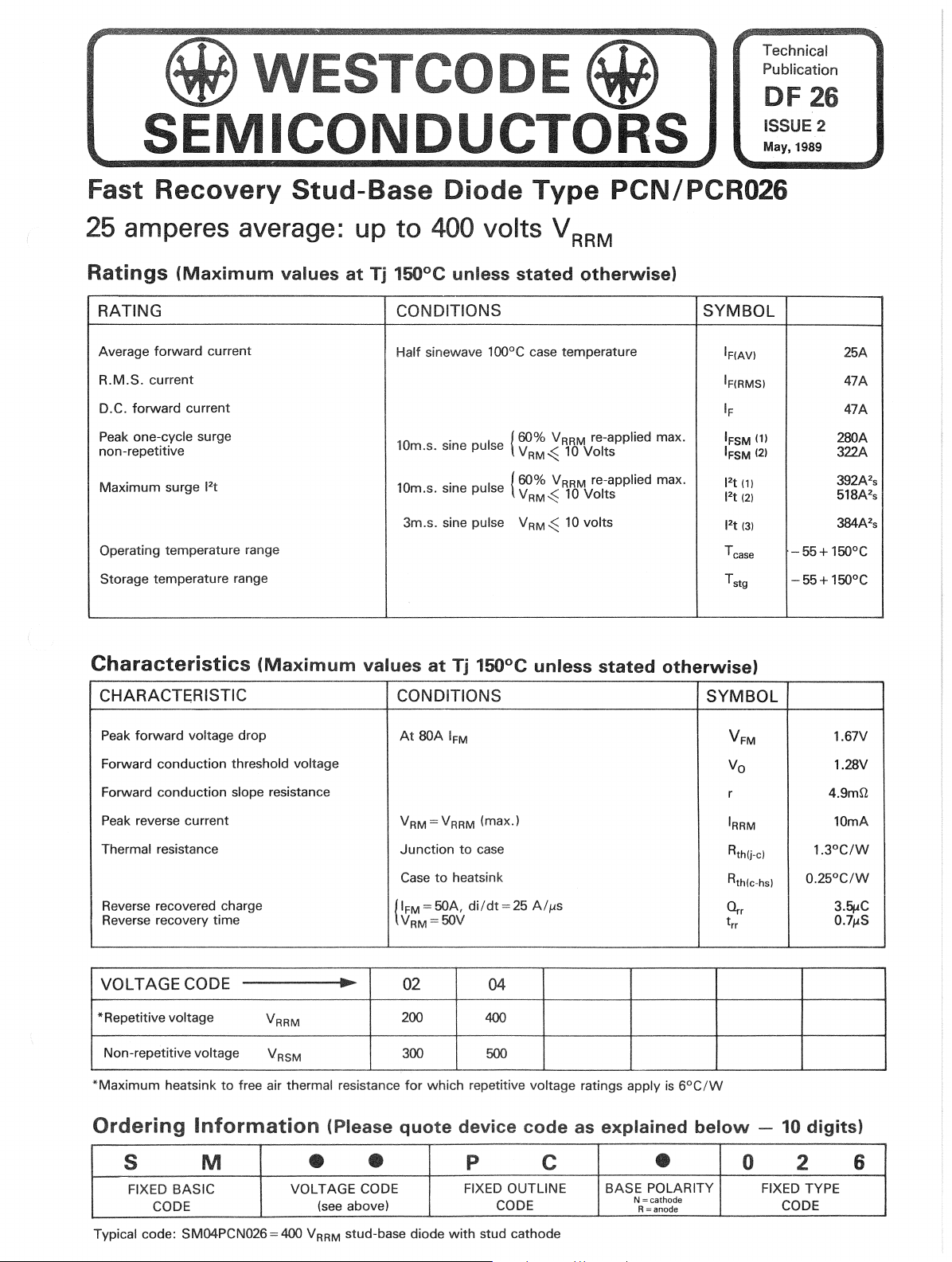
Ratings
RATING
Average forward current
R.M.S. current
D.C. forward current
Peak
non-repetitive
Maximum surge 12t
Operating temperature range
Storage temperature range
Characteristics
(Maximum
one-cycle surge
values
(Maximum
up
to 400 volts V
at
Tj 150°C unless stated otherwise)
CONDITIONS
Half sinewave 100°C case temperature
10
10
values
. I { 60% V
sme pu
m.s.
m.s.
sme
3m.s. sine pulse
at
se
. I
pu
se
Tj 150°C unless stated otherwise)
V
{60%
VRM~
VRM~
~
RM""",
V
RRM
re-applied max.
RRM
10
Volts
re-applied max.
RRM
10
Volts
10
volts
SYMBOL
IF(AV)
IF(RMS)
IF
I
(1)
FSM
(2)
I
FSM
12t (1)
Ilt
(2)
12t
(3)
Tcase
T
stg
25A
47A
47A
2BOA
322A
392A
518A2
384A2s
-55+150oC
-55+
150°C
2
s
S
CHARACTERISTIC
Peak
forward voltage drop
V
RRM
V
voltage
...
RSM
Forward conduction threshold
CODE
to
slope resistance
free air thermal resistance
Forward conduction
Peak
reverse current
Thermal
Reverse recovered charge
Reverse recovery time VRM=50V
VOL
* Repetitive voltage
Non-repetitive voltage
*Maximum heatsink
resistance
TAGE
Ordering Information (Please
CONDITIONS
At
BOA
VRM=VRRM (max.)
Junction
Case
to
{IFM=50A,
02
200
300
for
which repetitive voltage ratings apply
quote
IFM
to
case
heatsink
di/dt=25
A/jJ.s
04
400
500
device code as explained
is
6°C/W
SYMBOL
V
FM
Vo
r
IRRM
R
thO
Rth(c-hs)
Orr
trr
below
1.67V
1.28V
4.9mQ
10mA
-c)
1.3°C/W
0.25°C/W
3.fil.iC
O.7Il
- 10 digits)
S
S
FIXED BASIC
CODE
Typical code: SM04PCN026 = 400 V
M
VOLTAGE CODE
•
(see above)
stud-base diode
RRM
•
p
FIXED OUTLINE
CODE
with
stud cathode
C
BASE POLARITY FIXED
•
N=cathode
R=anode
0
CODE
2
TYPE
6
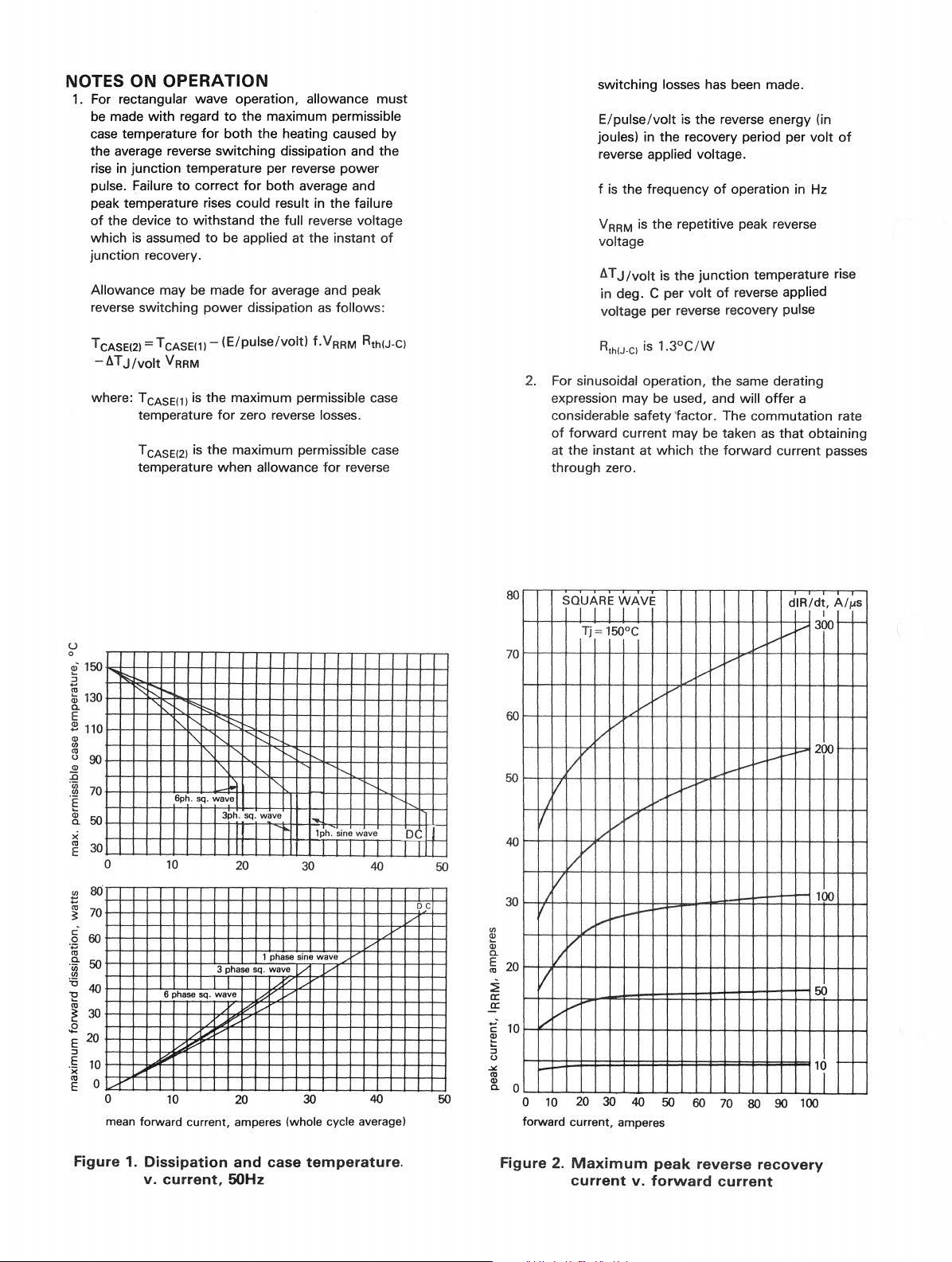
NOTES ON OPERATION
1. For rectangular
be made
case temperature
the
average reverse
rise in
junction
pulse. Failure
peak temperature rises
of
the device
which
is assumed
junction
Allowance may be made
reverse
recovery.
switching
wave
operation, allowance
with
regard
to
the
for
both
switching
temperature per reverse
to
correct
to
withstand
could
to
be applied
power
for
for
dissipation
the
the
maximum
heating caused
dissipation and
both
result in
full reverse voltage
average and peak
permissible
power
average and
the
at
the
instant
as
follows:
failure
must
by
the
of
switching
E/pulse/volt
joules) in
reverse applied voltage.
f
is
V
RRM
voltage
AT
in deg. C per
voitage
losses has been made.
is
the
reverse energy (in
the
recovery period per
the
frequency
is
the
J/vo!t
is
per reverse recovery pulse
of
operation in Hz
repetitive peak reverse
the
junction
volt
of
reverse applied
volt
of
temperature rise
T CASE(2) = T CASE(1) -
-ATJ/volt
where: T CASE(1) is
temperature
T CASE(2) is
temperature
u
o
(Xi
150
:;
~
a.
E
~
lJ)
co
'"
u
(I)
1i
'~
'E
Iii
a. 50
x
130
110
90
70
~
f::C'
E 30
o
t!
80
~
70
c·
o
60
''''
~
:~
50
~
40
~
30
£
E20
:::
,~
10
t,..
V
,....
1'1"'-
10
6 phase
k:;
~
IE/pulse/volt)
RRM
the
maximum
for
the
maximum
when
r"'~
R;
I"
i"-
1"-
1"-
1"-
sq.
wave
/~V'
~
I..)
3ph. sq. wave
3 phase sq, wave
6ph. sq. wave I
zero reverse losses.
allowance
t--..
f'.
~
I
I
20
1 phase sine wave
k:::
It:>"
V
E 0
o
mean forward current, amperes (whole cycle
10
20
f,VRRM
permissible case
permissible case
for
",f"
"-.
l"-
....
1ph. sine wave
i
30
V-
V
V
V
30
RthIJ-C)
reverse
i'-
,I--
40
V
V
40
average~
1-1-.
t--,
D-9
DC
2. For sinusoidal operation,
expression
considerable safety 'factor. The
of
forward
at
the
through
80
70
SQIU~RIIIVE
instant
Tj,='
may
be used, and will
current
at
zero,
150°C
which
,
V
vV'
I
//
i-I-
V
V-
/.v
/
' ,
r-
--
~I
60
I
i
V
1/
V
I
V
V
VV
I-
o
10
forward
1I
V
V
I
1,/
V
V
20 30 40 50 60 70 80 90 100
current, amperes
50
-
I--
50
50
<I'J
a;
'"
a.
~
~
rx:
rx:
C
~
:;
u
.:.<
~
C.
40
30
20
10
0
may
v
the
V
I
..--
the
same derating
be taken
forward
V
V
v
l-
r
offer
a
commutation
as
that
obtaining
current passes
dIR/dt,
300
1--)
.......
V
j.--'
200
I-
~
v
i-
100
50
11
I '
rate
AlIAs
I-- I--
l-
I--
l-
1
I--
Figure
1.
Dissipation
v.
current.
and
50Hz
case
temperature.
Figure
2.
Maximum
current
peak
v.
forward
reverse
current
recovery

c
.,
::t
...
o
>
Q;
'"
"S
a.
--...
>-
Ol
Q;
a5
10
0.5
0.3
a.
5
3
1
I---
SQUARE
I---
Tj(initial) = 150°C
rate
of
change
3
WAVE
I
5
of
current,AI
d
10
- REVERSE
1
~v
vV'
I
I
30
50
f'S
LOSSES-
/'"
../
---
100
i--"
I--
-
I
IFM,A;-
300
1
09
1
Isd
I'j
25
1
16
II
5
~
1_
I
I
U
a
...
~
--...
5l
"S
a.
'ID
.~
~
:;
ro
~
~
....
0.1
0.05
0.03
0,01
0.005
0.003
0.001
L
1
f-.--SQUARE
3 5
rate
of
change
WAVE
~
of
current,
Tj (initial)
#.-
';/
~
10
/
AI
vV'
k:!:;:
30
f'S
150°C
50
'/
[7
~
t:::::
100
V
V
i.--
I--
./
300
IFMA
"
100
I I
r<l
20
I I
,1Q
5
:....!..
Figure
100
50
30
10
5.
u 3
::t
0;
Ol
m
..c
~
0.5
OJ
0.3
~
o
u
0.1
~
Figure
IFM \
IRM-
1--.
I----
1-.
10
rate
3.
a
of
5.
Max.
change
\
:..c,<-
Qrr~
~0.9
..---:::.
__
t==-
--t-.
20
30
change
Max.
change
energy/pulse/volt
of
SQUARE
I
I
.rVr
0.5
~
8
reverse
,/
...-l-
WAVE
Tj
=25°C
f..----
. "
~
current
~
--
~·~t-·--t'-'
100
50
of
current, AI/As
recovered
of
charge
current
v.
.
'F=t
v.
--
300
rate
rate
IFM,A
-
f-.
of
,
1_,
I
100
50
l-
I
25,
~o+-
5 .
of
-
~
I
Figure
100
50
30
Figure
4.
Junction
rate
r===
>--.
f..-.
>---
f-.,
I--/
~
~-""
t:::=----
rate
of
change
6.
of
change
f--
!
'-
-",'
......
V_
V
~.
V-
:.--::"
30
of
Max.
change
temperature
of
f-
SQTJARE
Ti
I
....
---
l-
J.-!-
--
50 100
current, AI/As
recovered
of
current
rise/pulse/volt
reverse
WAVE
150°C
V
l-
--
current
iFM,A,
~
--
f-l0
--
.J
300
v.
rate
100
I
50
25'
I
I
v"
,
l-
I
of
rate
Figure
of
change
7.
Max.
change
of
current,
reverse
of
AI
f'S
recovery
CUffeot
time
II.
rate
of
en
'1.
a.i
,g
C
QJ
0.5
>
0
Q
0,3
:!?
QJ
2:!
QJ
>
~
0.1
figure
I---
rate
i-
3 5 10
of
change
8.
Max.
change
of
current,
reverse
of
30
AI
IlS
recovery
current
50
t-.
t--
~'
100
time
v.
IFM.A
100-
---
-::::
"
300
rate
~
2S
10
•
r
of

10
~
U
a
(.)
<1'
c:
rn
"l6
0.1
Q.
.S
""iii
E
Q;
-:5
0.01
Figure
'/
0.0001
time,
I
I
0.001 0.01
seconds
9.
Junction
impedance
/'"
-
I
/'
I
0.1
to
case
transient
-
,
thermal
10
1000
w
'"
OJ
n.
E
CO
...
100
c
E':
:;
(.)
-0
m
~
.E
If)
::l
0
Q)
c:
~
c
rn
ti
.!:
Figure
-I-
,
10
150°C
1
/n
0.5 0.7 0.9
max. instantaneous forward
10.
Forward
-
-'
I
VV
25°C
/
voltage
r
I I
,
tt
I
)'"
1.1
1.3 1.5 1.7 1.9 2.1
voltage, volts
characteristic
>
~ii.':
~
..
=
i
~j..;p..
i-"r-
of
limit
diode
(j)
~
Q)
Q.
E
~
.:L
C
~
=s
(.)
Q)
OJ
:;
III
Q)
c:
'iii
~
'"
J::
.:L
]i
'"
0.
'"
2
0.5
0.1
0.05
0.01
f...-.----
----
i
v
f--
---
::::::::::::
-~
1
,
I
m.secs
-'
10
-
---...
L
--
0.51
duration
of
r---::--
V
5
surge
(i'11:
JR~~~\b\
.~'"1
V
V
r><
/r--
.
'~tl~'~r
IIFSM:
i--.
VflRM<101
(lFSM: 60% VRR
I
10
cycles
60Hz
50
100
at
,-
-r-rTrn
1
10'
103
10
(j)
<J
Q)
W
N
'"
0.
E
E
E
::l
E
'x
2
'"
:2
Figure
11.
Max.
initial
02.3
(.99)---'.
","_~
(.43)
00-
In
the
interest
______
SEMICONDUCT~
of
product
improvement,
I:,;:'1'.'J33;]
EST DE
Westcode
non-repetitive
junction
0.35
surge
temperature
IT.ffi1
I
·-"-1
-
U-iO,3:UNf.2A
"
reserves the
•
~
~
WESTCODE SEMiCONDUCTORS
P.O,
Wiltshire,
Telephone: (0249) 444524
Telex: 44751 Telefax: (0249) 659448
Box
right
57,
England
current
at
1SOoc
Dimensions in
Mounting
2-2.37
Threads
torque:
Nm
(0.207-0.242
not
to
Weight: 5 grams
to
change specifications at
Chippenham,
SN151JL
m.m.
(inches)
be lubricated
any
Kgf m)
time
without
UMITED
notice.
1
KSAC589
 Loading...