

~WESTCODE~
SEMICONDUCTORS
... May, 1989
Technical
Publication
OF
13
ISSUE 2
Fast
12
Ratings
RATING
Average forward current
R.M.S. current
D.C. forward current
Peak
non-repetitive
Maximum surge
Operating temperature range
Storage temperature range
Recovery
Stud-Base
amperes average: up
(Maximum
one-cycle surge
2
1
t
values
at
Tj 150°C
Diode
to
400 volts V
unless
CONDITIONS
Half sinewave 120°C
10
10
. I
sme
pu
. I
sme
pu
se
se
m.s.
m.s.
3m.s. sine pulse
{60%
{60%
Type
stated
case
temperature
V
RRM
VRM~
V
RRM
V
~
RM"
V
<
RM
PCN/PCR013
RRM
otherwise)
re-applied max.
10
Volts
re-applied max.
10
Volts
10
volts
SYMBOL
'FIAV)
i
)
FIRMS
IF
i
(1)
FSM
'FSM
(2)
2
1
t (1l
12t
(2)
J2t
{31
Tease
T
stg
-55+
-55+
12A
47A
47A
210A
240A
221A2s
288A~
2
213A
s
150°C
150°C
Characteristics
CHARACTERISTIC
Peak
forward voltage drop
Forward conduction threshold
Forward conduction slope resistance
Peak
reverse current
Thermal resistance Junction to
Reverse recovered charge
Reverse recovery time
VOL
T AGE CODE
Repetitive voltage
Non-repetitive voltage
Ordering
Information
(Maximum
voltage
...
VRRM
V
RSM
(Please
values
CONDITIONS
At
40A
V
RM
Case
{IFM
=50A,
V
RM
02
200
300
quote
at
==
V
to
=50V
Tj
150°C
IFM
(max.)
ARM
case
heatsink
di/dt=25
500
device
04
400
unless
A/fiS
code
stated
as
explained
otherwise)
SYMBOL
V
FM
Vo
r
IRRM
Rth(j-c)
Rthfc-hsl
Orr
trr
below
- 10
1.32V
0.95V
9.2mQ
10mA
2°C/W
0.25°C/W
3j.tC
O.6,.IS
digits)
CODE
M
I
I
S
FIXED BASIC
Typical code: SM04PCN013 =
•
VOLTAGE
(see
400
Vr:lRM
•
CODE
abovel
stud-base diode with stud cathode
FIXED OUTLINE BASE POLARITY
CODE
p
C
•
N=cathooo
R=.node
0
FIXED
CODE
1
TYPE
3
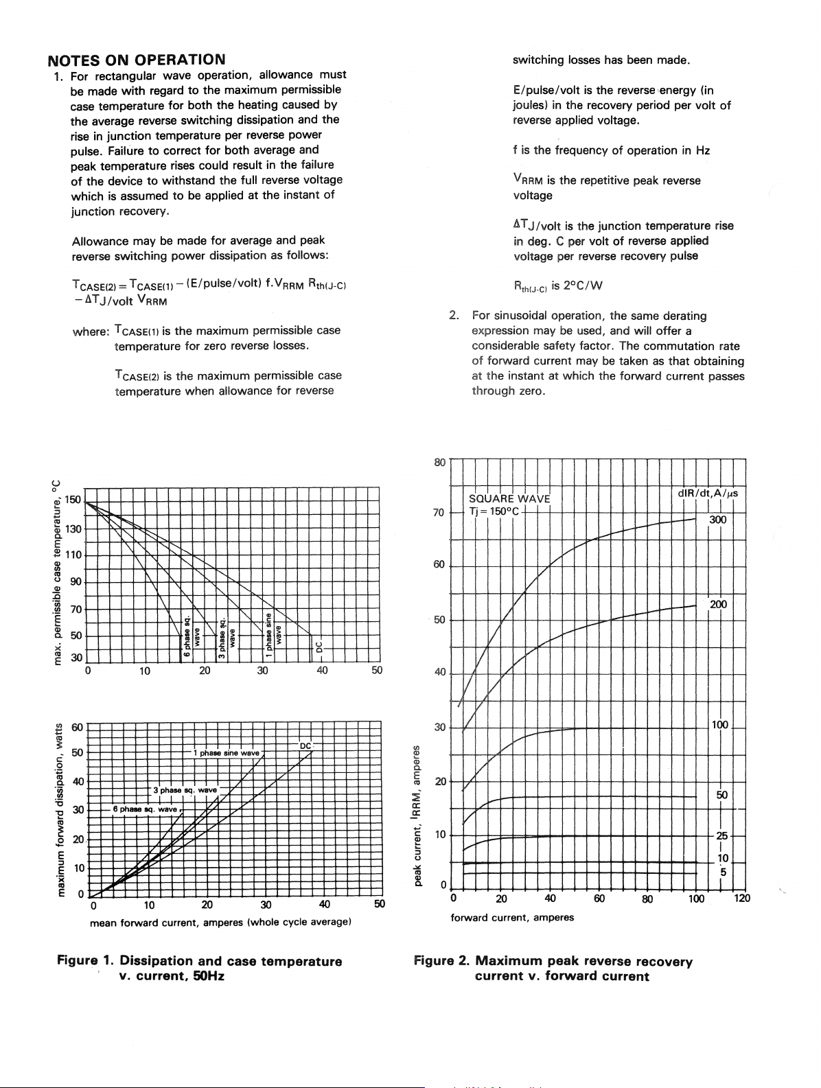
NOTES
1.
ON
OPERATION
For rectangular wave operation, allowance
be made
case temperature
the
rise
pulse. Failure
peak temperature rises could result in the failure
of
which
junction recovery.
Allowance may
reverse
with
regard
to
the maximum permissible
for
both the heating caused
average reverse switching dissipation and
in
junction
the device
is
temperature per reverse
to
correct
to
withstand the full reverse voltage
assumed
switching
to
be applied at the instant
be
made
power
for
both
average and
for
average and peak
dissipation
as
must
power
follows:
by
the
of
switching losses has been made.
E/pulse/volt
joules) in the recovery period per
reverse applied voltage.
f is the frequency
VF\RM
voltage
AT
J
/volt
in
deg. C per
voltage
is
the reverse energy (in
of
operation in Hz
is
the repetitive peak reverse
is
the junction temperature rise
volt
of
reverse applied
per reverse recovery pulse
volt
of
T CASE(2) = T CASE(1) -
-ATJ/volt
where: T
(J
o
~
150
E
..
Q;
130
c.
E
~
110
:g
..
'-'
90
v
2l
:~
70
E
"'I;;::..
V
RRM
eASE
temperature for zero reverse
T CASE(2)
temperature when
0. ...
,"-.,
f'::
\
1\
I'c
~50
><
E 30
o
~
60
~
c'
50
.£1
~40
" I
30
r-r-
"
~
.E
20
E
E 10
')(
E 0
o
mean
6
phase
forward
10
sq. wave
10
IE/pulse/volt)
!l)
is the maximum permissible case
is
the maximum permissible case
allowance for reverse
"
",,"-
"
1\
\
g:-
r;-,\
\;
_L
current, amperes (whole cycle average)
i
ii;-'
~
i
c.
.,
~-
'"
20
1 phase sine wove
.
i'
~
""
~
r-
~
I-
"-
~
f-!
f--B.
30
30
f,VRRM RthIJ-C)
losses.
.&
i
""
u
-
--
0
DC
40
----
50
50
2. For sinusoidal operation, the same derating
expression may be used, and will offer a
considerable safety factor. The commutation rate
of
forward
at
the
through
sIQ0AIR~
~
Tj
70
00
= 150°C
I I
I
V
V
II
/
V
II
30
I
current may
instant at which the forward current passes
zero.
I
i
I
be
taken
as
I
JvA~~
,-
i-
--
....-i-
I--""
V-
./
/
V
I
V
/
y
/
V
i-
/1--'
-
~
.---
I--
-..-
l-
V
,......
V
V
--
o
o
forward current, amperes
60
80
that
obtaining
l
dlR/dj'j/l-'S
f-
l-
I-
-
100
300
200
100
!jO
1 -
10
-
I
-
5
1
120
Figure
1.
Dissipation
v.
current,
and
50Hz
case
temperature
Figure
2.
Maximum
current
peak
v.
forward
reverse
current
recovery

10
5
3
~-
o
2::
0.5
'"
'"
g,
0.3
;,.
---
0>
:n
:r;
0.1
Figure
~
SQUARE WAVE -
;-
Tj(initiai) = 150°C
3 5
rate
of
change
3.
Max.
energy/pulse/volt
change
REVERSE
~
10
of
current,A/l's
of
reverse
V
./
~
V
---
30
current
LOSSES-
V
--
I
50
100
v.
L
rate
1-".
./
k--:
of
.IFM
300
A
100
~I
215
I
lp
5
0.05
0.03
u
°
,.;
g
~
0.01
g,
---
ffi
0.005
.;::
~
0.003
E
~
<lJ
C.
E
~
0.001
Figure 4.
0.1
!-
SQUARE
~
Ti
(initiali='150bC
- •
'1
rate
of
change
WAVE
I'
5
3
of
Junction
rate
of
,
~
~
10
current,
AI
temperature
change
of
~
f/"
50
30
flS
reverse
IFM,A
1~E
/'
V-
V
I?
____
,----
100
rise/pulse/volt
current
i~~
10
I
5-
---
f-
!
300
v.
100
50
30
10
rlgure
~SQUARE
f-
Tj
--150°C
5.
of
change
Max.
3 5
rate
change
WAVE
~
f:::-
~
10
of
current,
recovered
of
current
V
I--
~
I-
-
30
AI
fls
charge
50
100
v.
L
--
rate
./
!---"
I--
300
of
IFM.A
100
II
50
25
',d
5
10
5
3
:::'l
'"
III
.§
C'
0.5
~
~
i
...
0.1
rate
Figure
SQUARE WAVE
Tj
150°C
1 3 5
of
change
6.
Max.
reverse
change
~
of
current,
of
~
I:"-
10
AI
recovery
current
_"'S
r-
r.,.,
3050
flS
~
100
t,me
----
::----.
I'---
..........
r:::
300
v.
rate
IFM.A
100
I I
50
25
11~
of

10
~
.....
(,)
°
~
c:
CD
~
0.1
~
.s
10
E
CD
.s
0.01
0.0001
time, seconds
Figure 7.
0.001
Junction
to
impedance
0.01
case
III
I!!
CD
Co
E
CII
~
C
I!!
:s
<.>
CD
III
·iii
!!::
.t:.
""'
!
g
transient
0.5
~
:::I
0.1
CD
c:
0.05
CD
l
0.01
~
0.1
...........
~
V
1
thermal
........
---
m.S8CS
10
I--
0.5 1
duration
gJ1000
~
E
CII
""
150°C I
Y
10
FigureS.
:::::::
/'
5
10
of
surge
0.5 0.7 0.9
max. instantaneous forward
Forward
diode
../
::::-
cycles
at 50Hz
V
50
I
voltage
11'1:
VRRM<101
IIi:
ii
IIFSM: VRRM<
IIFSM: 80%
100
25°C
II
1.1
voltage, volts
characteristic
iilt1·
103
VR
2
10
1.3
~
III
E
:::I
E
·x
CII
::!:
1.5 1.7 1.9
of
limit
Figure 9.
In the interest
of
product improvement, Westcode reserves the right to change specifications at any time without notice .
••••••••
WESTCODE
SEMICONDUCTORS
Max.
initial
DO-
4
:r;M33il.
~
~
non-repetitive
junction
surge
temperature
current
150°C
at
Dimensions in m.m. (inches)
lYIounting torque:
2-2.37
Threads not
Nm
(0.207-0.242
to
be
Kgf
lubricated
Weight: 5 grams
WESTCODE SEMICONDUCTORS LIMITED
P.O.
Box
57,
Chippenham,
Wiltshire, England SN151JL
Telephone:
Telex: 44751 Telefax:
(0249) 444524
(0249) 659448
m)
~.
 Loading...