WeatherFlow WXFLW001 User Manual

User Manual
WF-RF915
,))/* '+7(=>,2=
/) =>,2=
1 Description
The WF-RF915 SOC RF module contains a 32-but ARM® Cortex®-M4 core with 32 kB ram and
256 kB flash running at 38.4 Mhz. The built in 915Mhz @ 7.4dBm radio has the capability to
transmit over long distances using little power.
2 Application
Smart Weatherstation Control and Communications.
3 Features
● 32-bit ARM® Cortex®-M4 core
● Autonomous Hardware Crypto Accelerator and Random Number Generator
● Integrated balun for 7.4 dBm transmit power
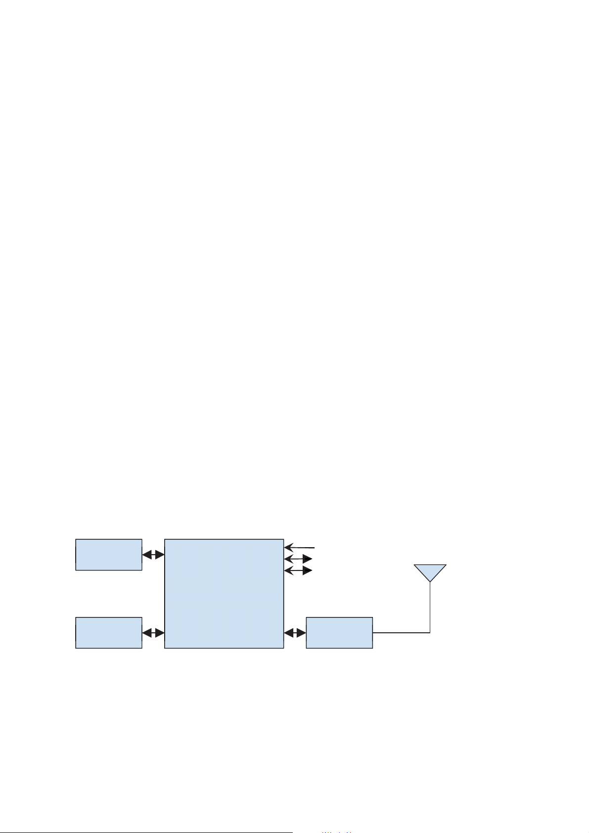
4 Block Diagram
8 MiB Flash
(optional)
EFR32FG
OSC
38.4 Mhz
VCC
I2C (x1)
GPIO (x10)
RF Front End
External Antenna

5 Pin Description
Pin
No.
Signal Name
Type
Pin Name
Description
1
Ground
SIG
-
Ground
2
NC - -
3
I2C_SDA
IO
PD15
I2C #0 SDA
4
I2C_SCL
IO
PD14
I2C #0 SDC
5
Port A0
IO
PA0
GPIO 1
6
Port A1
IO
PA1
GPIO 2
7
Port B11
IO
PB11
GPIO 3
8
Port B12
IO
PB12
GPIO 4
9
Port B13
IO
PB13
GPIO 5
10
Ground
SIG
-
Ground
11
Ground
SIG
-
Ground
12
VCC 3.3
SIG
-
Power Supply 3.3v
13
Port C11
IO
PC11
GPIO 6
14
Port F0
IO
PF0
GPIO 7
15
Port F1
IO
PF1
GPIO 8
16
Port F2
IO
PF2
GPIO 9
17
Port F3
IO
PF3
GPIO 10
18
RESET
IO
NRST
RESET_N
19
NC - -
20
Ground
SIG
-
Ground
5.1 Pin Map

6 Electrical Specification
Parameter
Min Typ
Max
Storage Temperature Range
-
50 - 150
External main supply voltage
0 - 3.8
External main supply voltage ramp rate
- - 1
Voltage on any 5V tolerant GPIO pin
1
-
0.3
-
Min of 5.25 and
IOVDD + 2
Voltage on non-5V tolerant GPIO pins
-
0.3 - IOVDD + 0.3
V
Voltage on HFXO pins
-
0.3 - 1.4
V
Voltage differential between RF pins (2G4RF_IOP -
2G4RF_ION)
-50 - 50
mV
Absolute Voltage on RF pins 2G4RF_IOP and
2G4RF_ION
-0.3 - 3.3
V
Voltage differential between RF pins (SUBGRF_IP -
SUBGRF_IN)
-
50 - 50
mV
Absolute Voltage on RF pins SUBGRF_IP, SUBGRF_IN,
SUBGRF_OP, and SUBGRF_ON
-
0.3 - 3.3
V
Total current into VDD power lines (source)
- - 200
mA
Total current into VSS ground lines (sink)
- - 200
mA
Current per I/O pin (sink)
- -
50
mA
Current per I/O pin (source)
- - 50
Current for all I/O pins (sink)
- - 200
mA
6.1 Absolute Maximum Ratings
Stresses above those listed below may cause permanent damage to the device. This is a stress
rating only and functional operation of the devices at those or any other conditions above those
indicated in the operation listings of this specification is not implied. Exposure to maximum
rating conditions for extended periods may affect device reliability.
Table 6.0
Unit
°C
V
V / μs
V
mA
 Loading...