

Wavecom Q2501 Customer Design Manuallines

WISMO Quik Q25 series
WISMO Quik Q2501
Customer Design Guidelines
Reference : WM_PRJ_Q2501_PTS_002
Revision : 001
Date : March 2004
confidential ©
This document is the sole and exclusive property of WAVECOM. Not to be distributed or divulged
without prior written agreement.
Ce document est la propriété exclusive de WAVECOM. Il ne peut être communiqué ou divulgué à
des tiers sans son autorisation préalable.
Page :
1 / 79

WM_PRJ_Q2501_PTS_002 - 001
March 2004
Document Information
Revision Date History of the evolution
001 March 04 Preliminary version
confidential ©
This document is the sole and exclusive property of WAVECOM. Not to be distributed or divulged
without prior written agreement.
Ce document est la propriété exclusive de WAVECOM. Il ne peut être communiqué ou divulgué à
des tiers sans son autorisation préalable.
Page: 2 / 79

WM_PRJ_Q2501_PTS_002 - 001
March 2004
Overview
The WISMO Quik Q2501 module is an E-GSM/DCS - GPRS 900/1800 MHz dual
band module with 16 channels GPS receiver. It is dedicated to automotive
applications, driven by AT commands.
The WISMO Quik Q2501 memory configuration is:
GSM/GPRS part: 32 Mbits of Flash memory and 4 Mbits of SRAM,
GPS part: 8 Mbits of Flash memory.
This document gives recommendations and general guidelines to design an
application using the WISMO Quik Q2501 module.
It gives some recommendations for:
Base Band design rules and typical implementation examples,
RF design rules and typical implementation examples,
Mechanical constraints for module fitting,
PCB routing recommendations,
Test and download recommendations.
It also recommends some manufacturers and suppliers for the peripheral
devices which can be used with the WISMO Quik Q2501 modules.
For further information about the WISMO Quik Q2501 module, refer to the
Product Technical Specification (document [2]).
confidential ©
This document is the sole and exclusive property of WAVECOM. Not to be distributed or divulged
without prior written agreement.
Ce document est la propriété exclusive de WAVECOM. Il ne peut être communiqué ou divulgué à
des tiers sans son autorisation préalable.
Page: 3 / 79

WM_PRJ_Q2501_PTS_002 - 001
March 2004
Contents
Document Information......................................................................... 2
Overview ............................................................................................. 3
Contents.............................................................................................. 4
Table of figures ................................................................................... 6
Cautions .............................................................................................. 8
Trademarks ......................................................................................... 8
1 References.................................................................................... 9
1.1 Reference Documents .............................................................................9
1.2 Glossary ..................................................................................................9
1.3 Abbreviations ........................................................................................10
2 General Information .................................................................... 14
2.1 Features ................................................................................................14
2.2 Functional architecture..........................................................................16
3 Functional Design ....................................................................... 17
3.1 Power supply part .................................................................................17
3.1.1
3.1.2
3.2 Common GSM/GPS part........................................................................22
3.2.1
3.2.2
3.2.3
3.2.4
3.3 GSM/GPRS Base Band part ...................................................................25
3.3.1
3.3.2
3.3.3
3.3.4
3.3.5
3.3.6
3.3.7
3.3.8
3.3.9
3.3.10 GSM Base Band Activation indicator .............................................45
3.3.11 External Interrupt...........................................................................45
3.3.12 Auxiliary Analog Signals ................................................................46
3.4 GPS Base Band part ..............................................................................47
3.4.1
This document is the sole and exclusive property of WAVECOM. Not to be distributed or divulged
without prior written agreement.
Ce document est la propriété exclusive de WAVECOM. Il ne peut être communiqué ou divulgué à
des tiers sans son autorisation préalable.
Main power supply and ground plane ...........................................17
RTC Back-up supply ......................................................................20
Module activation function (ON/~OFF)...........................................22
Alternative download control function (BOOT)...............................22
Reset function (~RST)....................................................................23
Activity status indication function (FLASH_LED & GPS_TIMEPULSE)24
GSM serial links.............................................................................25
General purpose I/O .......................................................................28
Peripheral buses ............................................................................29
SIM interface .................................................................................31
Keyboard interface.........................................................................35
Audio interface ..............................................................................37
Buzzer interface.............................................................................43
Digital Power Supply for External Devices (VCC)............................44
GSM transmission activity status ..................................................44
GPS activation function .................................................................47
confidential ©
Page: 4 / 79

WM_PRJ_Q2501_PTS_002 - 001
March 2004
3.4.2
3.4.3
3.4.4
3.4.5
3.4.6
3.5 RF part ..................................................................................................53
3.5.1
3.5.2
3.5.3
3.5.4
4 PCB Design ................................................................................. 60
4.1 General Rules and Constraints ..............................................................60
4.2 Specific Routing Constraints .................................................................60
4.2.1
4.2.2
4.2.3
4.2.4
4.2.5
4.3 Pads design...........................................................................................67
5 Mechanical Specifications .......................................................... 68
GPS serial links..............................................................................48
Dead reckoning interface ...............................................................50
1.8 V Digital Power Supply for External Devices ............................52
GPS External Interruption ..............................................................52
GPS Antenna Power Supply ..........................................................52
Antenna connection possibilities ...................................................53
GSM/GPRS antenna connection.....................................................54
GPS antenna connection ...............................................................55
Single coax connection..................................................................59
System Connector .........................................................................60
Power Supply ................................................................................60
SIM interface routing constraints...................................................62
Audio circuit routing constraints....................................................62
RF circuit routing constraints.........................................................63
6 EMC and ESD recommendations................................................. 70
7 Firmware upgrade requirements ................................................. 71
8 Embedded Testability.................................................................. 72
8.1 Access to the serial link.........................................................................72
8.2 RF output accessibility for diagnostic ....................................................74
9 Manufacturers and suppliers ...................................................... 75
9.1 System connector .................................................................................75
9.2 SIM Card Reader ...................................................................................75
9.3 Microphone...........................................................................................75
9.4 Speaker .................................................................................................76
9.5 RF cable ................................................................................................76
9.6 GSM antenna ........................................................................................76
9.7 GPS antenna .........................................................................................77
9.8 Buzzer...................................................................................................77
10 Appendix .................................................................................. 78
10.1 80-pin PCB receptacle ...........................................................................79
confidential ©
This document is the sole and exclusive property of WAVECOM. Not to be distributed or divulged
without prior written agreement.
Ce document est la propriété exclusive de WAVECOM. Il ne peut être communiqué ou divulgué à
des tiers sans son autorisation préalable.
Page: 5 / 79

WM_PRJ_Q2501_PTS_002 - 001
March 2004
Table of figures
Figure 1: Functional architecture .................................................................... 16
Figure 2: Typical Power supply voltage in GSM/GPRS mode .......................... 18
Figure 3: RTC supplied by a super capacitor................................................... 20
Figure 4: RTC supplied by a non rechargeable battery.................................... 21
Figure 5: RTC supplied by a rechargeable battery cell .................................... 21
Figure 6: Example of ON/~OFF pin connection ...............................................22
Figure 7: Example of BOOT pin connection ....................................................22
Figure 8: Example of ~RST pin connection..................................................... 23
Figure 9: Example N°1 of GSM and GPS activity status implementation......... 24
Figure 10: Example N°2 of GSM activity status implementation .....................24
Figure 11: Example of RS232 level shifter implementation for GSM UART1 ... 25
Figure 12: Example of V24/CMOS serial link implementation for UART1 ........26
Figure 13: Example of RS232 level shifter implementation for GSM UART2 ... 27
Figure 14: Example of SPI bus application...................................................... 29
Figure 15: example of 2 wire bus application ................................................. 30
Figure 16: Example of 3V SIM Socket implementation.................................... 31
Figure 17: Example of 1.8 V / 3 V SIM interface implementation ....................33
Figure 18: Example of 3 V / 5 V SIM interface implementation .......................34
Figure 19: Example of keyboard implementation ............................................ 36
Figure 20: Example of main microphone (MIC2) implementation.................... 38
Figure 21: MIC1 input differential connection................................................. 39
Figure 22: MIC1 input single ended connection ............................................. 40
Figure 23: Speaker differential connection ...................................................... 41
Figure 24: Speaker single-ended connection .................................................. 42
confidential ©
This document is the sole and exclusive property of WAVECOM. Not to be distributed or divulged
without prior written agreement.
Ce document est la propriété exclusive de WAVECOM. Il ne peut être communiqué ou divulgué à
des tiers sans son autorisation préalable.
Page: 6 / 79

WM_PRJ_Q2501_PTS_002 - 001
March 2004
Figure 25: Example of buzzer implementation ................................................ 43
Figure 26: LED driven by the BUZ output ....................................................... 43
Figure 27: ~INTR driving example .................................................................. 45
Figure 28: Example of ADC application........................................................... 46
Figure 29: GPS activation function implementation ........................................ 47
Figure 30: Example of RS232 level shifter implementation for GPS UART2 .... 48
Figure 31: Example of RS232 level shifter implementation for GPS UART0 .... 49
Figure 32: SPI interface implementation for the dead reckoning function .......50
Figure 33: Block diagram of the GPS antenna connection ..............................55
Figure 34: GPS reception jammed by GSM/GPRS transmission...................... 57
Figure 35: Example of Q2501 module and GPS antenna integrated application
...................................................................................................................... 58
Figure 36 :Example of power supply routing .................................................. 60
Figure 37: Burst simulation circuit.................................................................. 61
Figure 38: AppCad Screenshot for MicroStrip design ..................................... 63
Figure 39: Example of PCB routing for pigtail connection ............................... 66
Figure 40: Pads design................................................................................... 67
Figure 41: GSM UART1 serial link debug access ............................................ 72
Figure 42: Module connection for RF measurements...................................... 74
confidential ©
This document is the sole and exclusive property of WAVECOM. Not to be distributed or divulged
without prior written agreement.
Ce document est la propriété exclusive de WAVECOM. Il ne peut être communiqué ou divulgué à
des tiers sans son autorisation préalable.
Page: 7 / 79

WM_PRJ_Q2501_PTS_002 - 001
March 2004
Cautions
Information furnished herein by Wavecom are accurate and reliable. However
no responsibility is assumed for its use. Please read carefully the safety
precautions for an application based on a WISMO Quik Q2501 module.
In addition, Wavecom reserves the right to modify this information with an aim
of improving the accuracy of information provided herein.
General information about Wavecom and its range of products is available at
the following internet address: http://www.wavecom.com
Trademarks
WAVECOM and WISMO are trademarks or registered trademarks of Wavecom
S.A. All other company and/or product names mentioned may be trademarks or
registered trademarks of their respective owners.
confidential ©
This document is the sole and exclusive property of WAVECOM. Not to be distributed or divulged
without prior written agreement.
Ce document est la propriété exclusive de WAVECOM. Il ne peut être communiqué ou divulgué à
des tiers sans son autorisation préalable.
Page: 8 / 79

WM_PRJ_Q2501_PTS_002 - 001
March 2004
1 References
1.1 Reference Documents
[1] Automotive Environmental Control Plan for WISMO Quik Q2501
WM_PRJ_Q2501_DCP_001
[2] WISMO Quik Q2501 Product Technical Specification
WM_PRJ_Q2501_PTS_001
[3] WISMO Quik Q2501 Process Customer Guidelines
WM_PRJ_Q2501_PTS_003
1.2 Glossary
Term Definition
Performing a FIX Means the GPS receiver is able to compute a
position
Dead reckoning GPS Feature that allows navigation with poor/no
satellites view by the aid of external sensors that
provide course (odometer) and heading
(gyroscope).
Single Coax WAVECOM concept that allows the user to use
only one single coaxial cable for both GSM and
GPS RF signal to connect the WISMO Quik Q2501
module to the antennas.
The antennas are most of the time physically
distinct but connected to the WISMO Quik Q2501
module by a single coaxial cable through an
antenna switch system, saving a second coaxial
cable.
Cold Start
Powering up a unit after it has been turned off for
an extended period of time and no longer contains
current ephemeris data. In Cold Start Scenario, the
receiver has no knowledge on last position,
approximate time or satellite constellation. The
receiver starts to search for signals blindly. This is
normal behavior, if no backup battery is connected.
Cold Start time is the longest startup time for GPS
receivers and can be several minutes.
confidential ©
This document is the sole and exclusive property of WAVECOM. Not to be distributed or divulged
without prior written agreement.
Ce document est la propriété exclusive de WAVECOM. Il ne peut être communiqué ou divulgué à
des tiers sans son autorisation préalable.
Page: 9 / 79

WM_PRJ_Q2501_PTS_002 - 001
March 2004
Term Definition
Hot Start
Warm Start
Coarse Acquisition
Code (C/A Code)
Start mode of the GPS receiver when current
position, clock offset, approximate GPS time and
current ephemeris data are all available. In Hot
Start Scenario, the receiver was off for less than
2 hours. It uses its last Ephemeris data to calculate
a position fix.
Start mode of a GPS receiver when current
position, clock offset and approximate GPS time are
known. Almanac data is retained, but the
ephemeris data is cleared. In Warm Start Scenario,
the receiver knows - due to a backup battery or by
other techniques – his last position,
approximate time and almanac. Thanks to this, it
can quickly acquire satellites and get a
position fix faster than in cold start mode.
The standard positioning signal the GPS satellite
transmits to the civilian user. It contains the
information the GPS receiver uses to fix its position
and time. Accurate to 24 meter. This code is a
sequence of 1023 pseudorandom binary biphase
modulations on the GPS carrier (L1) at a chipping
rate of 1.023 MHz, thus having a code repetition
period of 1 millisecond. The code was selected to
provide good acquisition properties. Also known as
the "civilian code.".
1.3 Abbreviations
Abbreviation Definition
AC Alternative Current
ADC Analogue to Digital Converter
A/D Analogue to Digital conversion
AF Audio-Frequency
AT ATtention (prefix for modem commands)
AUX AUXiliary
CAN Controller Area Network
CB Cell Broadcast
CEP Circular Error Probable
CLK CLocK
confidential ©
This document is the sole and exclusive property of WAVECOM. Not to be distributed or divulged
without prior written agreement.
Ce document est la propriété exclusive de WAVECOM. Il ne peut être communiqué ou divulgué à
des tiers sans son autorisation préalable.
Page: 10 / 79

WM_PRJ_Q2501_PTS_002 - 001
March 2004
Abbreviation Definition
CMOS Complementary Metal Oxide Semiconductor
CS Coding Scheme
CTS Clear To Send
DAC Digital to Analogue Converter
dB Decibel
DC Direct Current
DCD Data Carrier Detect
DCE Data Communication Equipment
DCS Digital Cellular System
DR Dynamic Range
DSR Data Set Ready
DTE Data Terminal Equipment
DTR Data Terminal Ready
EFR Enhanced Full Rate
E-GSM Extended GSM
EMC ElectroMagnetic Compatibility
EMI ElectroMagnetic Interference
EMS Enhanced Message Service
EN ENable
ESD ElectroStatic Discharges
FIFO First In First Out
FR Full Rate
FTA Full Type Approval
GND GrouND
GPI General Purpose Input
GPIO General Purpose Input Output
GPO General Purpose Output
GPRS General Packet Radio Service
GPS Global Positioning System
GSM Global System for Mobile communications
HR Half Rate
I/O Input / Output
LED Light Emitting Diode
LNA Low Noise Amplifier
confidential ©
This document is the sole and exclusive property of WAVECOM. Not to be distributed or divulged
without prior written agreement.
Ce document est la propriété exclusive de WAVECOM. Il ne peut être communiqué ou divulgué à
des tiers sans son autorisation préalable.
Page: 11 / 79

WM_PRJ_Q2501_PTS_002 - 001
March 2004
Abbreviation Definition
MAX MAXimum
MIC MICrophone
MIN MINimum
MMS Multimedia Message Service
MO Mobile Originated
MT Mobile Terminated
NF Noise Factor
NMEA National Marine Electronics Association
NOM NOMinal
PA Power Amplifier
Pa Pascal (for speaker sound pressure measurements)
PBCCH Packet Broadcast Control CHannel
PC Personal Computer
PCB Printed Circuit Board
PDA Personal Digital Assistant
PFM Power Frequency Modulation
PSM Phase Shift Modulation
PWM Pulse Width Modulation
RAM Random Access Memory
RF Radio Frequency
RFI Radio Frequency Interference
RHCP Right Hand Circular Polarization
RI Ring Indicator
RST ReSeT
RTC Real Time Clock
RTCM Radio Technical Commission for Maritime services
RTS Request To Send
RX Receive
SIM Subscriber Identification Module
SMS Short Message Service
SPI Serial Peripheral Interface
SPL Sound Pressure Level
SPK SPeaKer
SRAM Static RAM
confidential ©
This document is the sole and exclusive property of WAVECOM. Not to be distributed or divulged
without prior written agreement.
Ce document est la propriété exclusive de WAVECOM. Il ne peut être communiqué ou divulgué à
des tiers sans son autorisation préalable.
Page: 12 / 79

WM_PRJ_Q2501_PTS_002 - 001
March 2004
Abbreviation Definition
TBC To Be Confirmed
TDMA Time Division Multiple Access
TP Test Point
TVS Transient Voltage Suppressor
TX Transmit
TYP TYPical
UART Universal Asynchronous Receiver-Transmitter
USB Universal Serial Bus
USSD Unstructured Supplementary Services Data
VSWR Voltage Stationary Wave Ratio
confidential ©
This document is the sole and exclusive property of WAVECOM. Not to be distributed or divulged
without prior written agreement.
Ce document est la propriété exclusive de WAVECOM. Il ne peut être communiqué ou divulgué à
des tiers sans son autorisation préalable.
Page: 13 / 79

WM_PRJ_Q2501_PTS_002 - 001
March 2004
2 General Information
2.1 Features
WISMO Quik Q2501 is self-contained E-GSM/DCS-GPRS 900/1800 dual-band
module with 16 bits GPS receiver.
Following table reminds the WISMO Quik Q2501 features:
Feature Information
Physical
characteristics
Size: 58.4 x 32.2 x 6.3 mm.
Weight: 11 g.
Complete shielding.
Module control Full set of AT commands for GSM/GPRS including
GSM 07.07 and 07.05 AT command sets.
Specific AT commands for GPS management on same
link as GSM/GPRS AT commands.
Direct reception of GPS data through serial link.
Status indication for GSM and for GPS functions.
GSM/DCS Frequency bands:
• Rx (E-GSM 900): 925 to 960 MHz.
• Rx (DCS 1800): 1805 to 1880 MHz.
• Tx (E-GSM 900): 880 to 915 MHz.
• Tx (DCS 1800): 1710 to 1785 MHz.
Transmit power:
• Class 4 (2 W) at E-GSM
• Class 1 (1 W) at DCS
GPRS GPRS multislot class 10.
Multislot class 2 supported.
PBCCH support.
Coding schemes: CS1 to CS4.
Voice Features GSM Voice Features with Emergency calls 112.
Full Rate (FR)/ Enhanced Full Rate (EFR) / Half Rate
(HR).
Echo cancellation and noise reduction.
Full duplex Hands free.
SMS SMS MT, MO and SMS CB
SMS storage into SIM card
confidential ©
This document is the sole and exclusive property of WAVECOM. Not to be distributed or divulged
without prior written agreement.
Ce document est la propriété exclusive de WAVECOM. Il ne peut être communiqué ou divulgué à
des tiers sans son autorisation préalable.
Page: 14 / 79

WM_PRJ_Q2501_PTS_002 - 001
March 2004
Feature Information
GSM Supplementary
Services
Call Forwarding, Call Barring.
Multiparty.
Call Waiting, Call Hold.
USSD.
Data / Fax Data circuit asynchronous, transparent, and non-
transparent up to 14400 bits/s.
Fax Group 3 compatible.
SIM interface 3 V only SIM interface.
1.8 & 5 V SIM interfaces are available with external
adaptation.
SIM Tool Kit Release 99.
GPS GPS L1 civil frequency 1575.42 MHz.
16 channels GPS receiver.
Accuracy:
• 2.5 m CEP.
• GPS 2 m CEP (depending on accuracy of
correction data); SBAS/WAAS supported.
Start-up times :
• Hot start: < 3.5 sec.
• Warm start: 33 sec.
• Cold start: 34 sec.
Signal reacquisition < 1 s.
Protocols:
• NMEA-0183 input/output.
• UBX binary input/output.
• RTCM in.
Interface available for Dead Reckoning.
Real Time Clock Real Time Clock with calendar and alarm.
RTC update with GPS information.
Temperature sensor Internal sensor for module temperature monitoring via
AT commands or embedded OpenAT application.
Advanced antennas
management
Single Coax connectivity.
GPS active antenna management (3 V / 5 V
compatible) with internal protection circuit.
Possible use of an auto-powered GPS active antenna.
confidential ©
This document is the sole and exclusive property of WAVECOM. Not to be distributed or divulged
without prior written agreement.
Ce document est la propriété exclusive de WAVECOM. Il ne peut être communiqué ou divulgué à
des tiers sans son autorisation préalable.
Page: 15 / 79
WM_PRJ_Q2501_PTS_002 - 001
March 2004
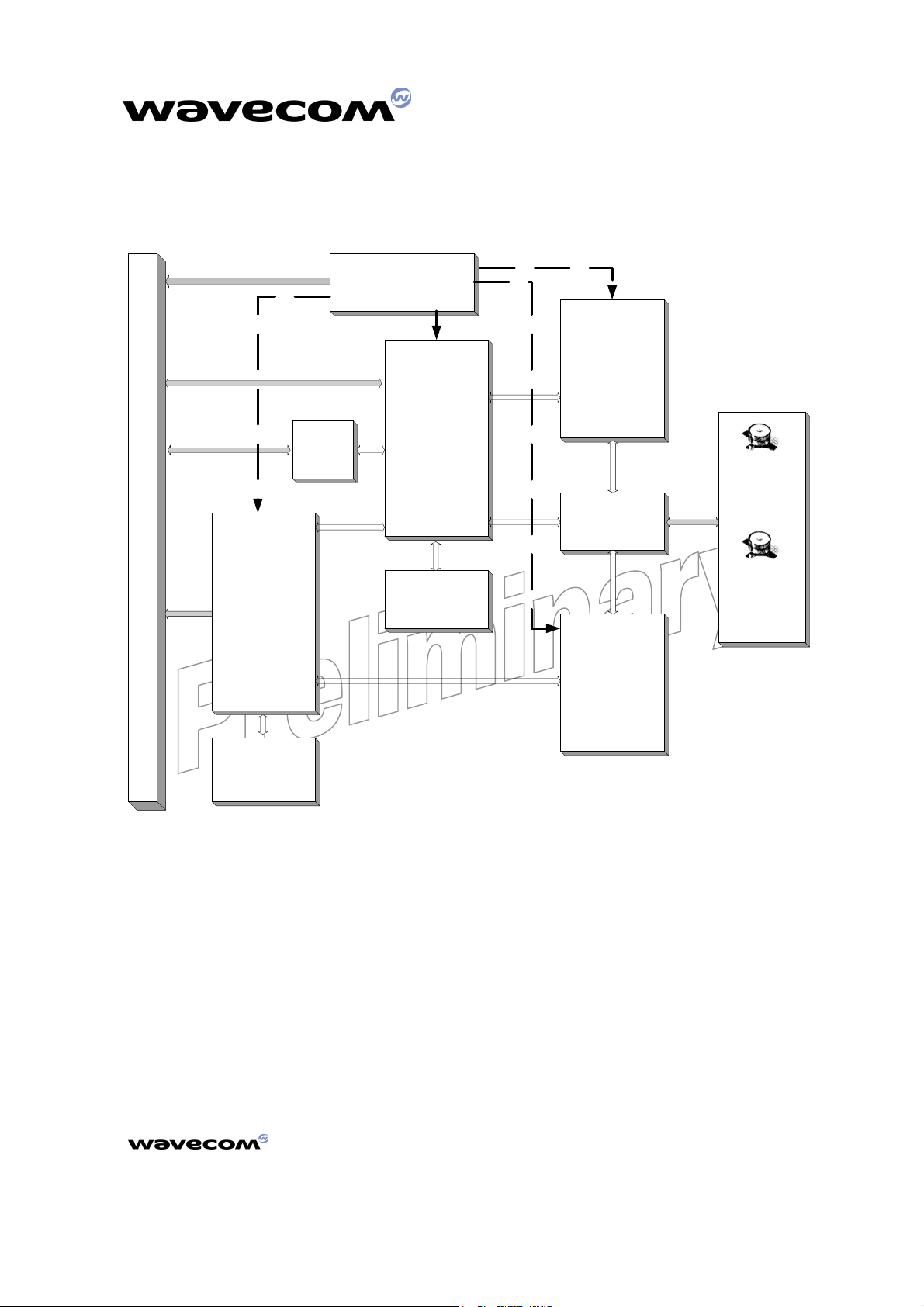
2.2 Functional architecture
POWER SUPPLY INTERFACE
W
I
S
M
O
Q
2
5
0
1
S
Y
S
T
E
M
C
N
N
E
C
T
O
R
BASEBAND
Audio filter
GPS
GSM / GPRS
BASEBAND
GSM Flash memory
RF GSM
FRONT END
ANTENNAS
CONTROL
RF GPS
FRONT END
GSM / GPS
ANTENNA
GPS
ANTENNA
RF PORTS
GPS Flash memory
Figure 1: Functional architecture
confidential ©
This document is the sole and exclusive property of WAVECOM. Not to be distributed or divulged
without prior written agreement.
Ce document est la propriété exclusive de WAVECOM. Il ne peut être communiqué ou divulgué à
des tiers sans son autorisation préalable.
Page: 16 / 79

WM_PRJ_Q2501_PTS_002 - 001
March 2004
3 Functional Design
Some of the WISMO interface signals are multiplexed in order to limit the
number of pins but this architecture implies some restrictions.
All external signals must be inactive when the WISMO module is OFF to avoid
any damage when starting the module.
3.1 Power supply part
3.1.1 Main power supply and ground plane
3.1.1.1 Electrical constraints
The main power supply (VBATT) is the only external power supply source used
to supply both the GSM/GPRS and GPS RF parts and Base Band parts.
The power supply is one of the key issues in the design of a GSM terminal.
Due to the bursted emission in GSM / GPRS, the power supply must be able to
deliver high current peaks in a short time (rising time is around 10 µs).
In communication mode, the GSM RF Power Amplifier current flows with a
ratio of (Figure 2):
• Max current 1/8 of the time (around 577 µs every 4.615 ms for
GSM/GPRS class 2 – 2RX / 1TX),
• Max current 2/8 of the time (around 1154 µs every 4.615 ms for
GSM/GPRS class 10 – 3RX / 2TX).
confidential ©
This document is the sole and exclusive property of WAVECOM. Not to be distributed or divulged
without prior written agreement.
Ce document est la propriété exclusive de WAVECOM. Il ne peut être communiqué ou divulgué à
des tiers sans son autorisation préalable.
Page: 17 / 79
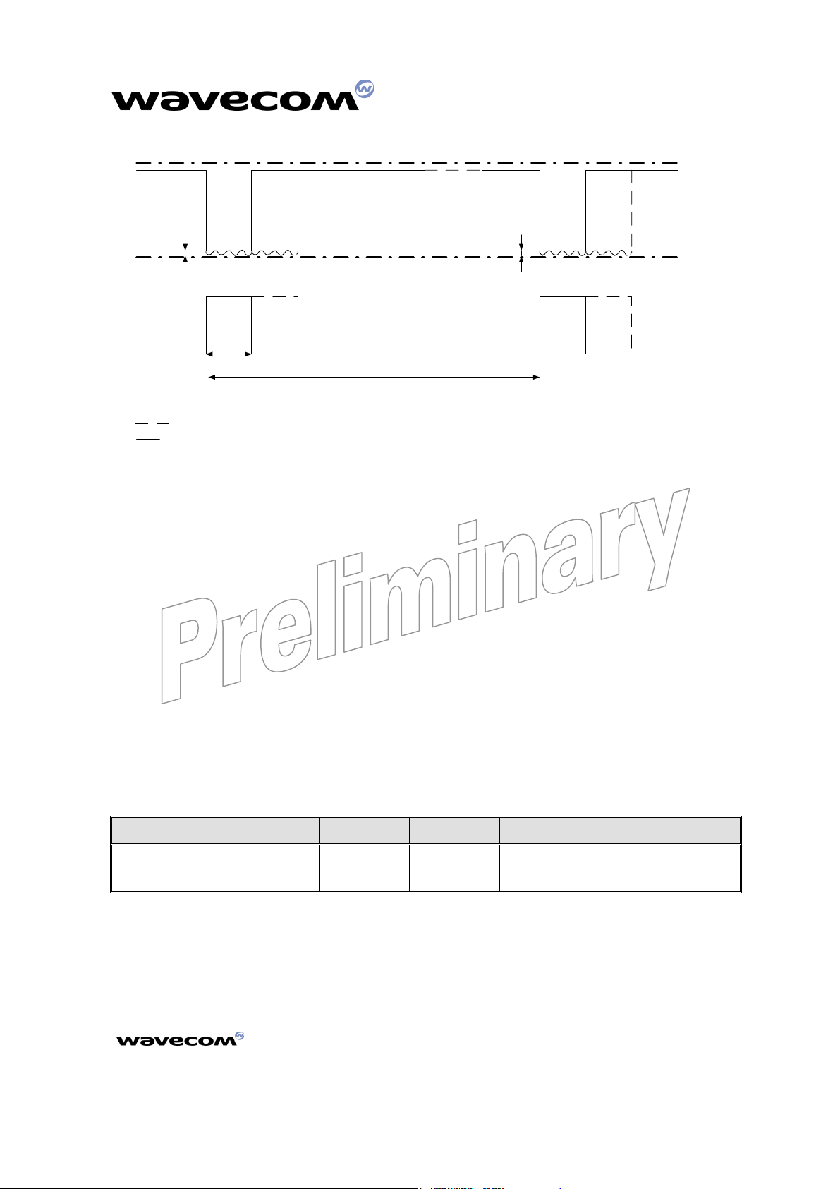
VBATT
WM_PRJ_Q2501_PTS_002 - 001
March 2004
Vmax
Uripp Uripp
IBATT
T=577µs
T = 4.615ms
Legend:
In GSM or GPRS class 2 modes
In GPRS class 10 mode
Vmin
Figure 2: Typical Power supply voltage in GSM/GPRS mode
During these peaks the ripple (U
) on the supply voltage must not exceed a
ripp
certain limit (refer to document [2]).
Because VBATT supplies directly the GSM RF power amplifier component, it is
essential to keep a minimum voltage ripple at this connection in order to avoid
any phase error or spectrum modulation degradation.
On the other hand, insufficient power supply voltage could dramatically affect
some RF performances: TX power, modulation spectrum, EMC (ElectroMagnetic Compatibility) performances, spurious emission and frequency error.
The power supply voltage features given in the table hereunder will guarantee
nominal functioning of the module.
Power Supply Voltage
V
VBATT
3.4 V (*) 3.6 V 4.5 V (**) 50 mVpp for freq<200 kHz
V
MIN
V
NOM
U
MAX
5 mVpp for freq>200 kHz
ripp
max
(*): This value has to be guaranteed during the burst (with 2.0 A Peak in GSM
or GPRS mode).
(**): max operating Voltage Stationary Wave Ratio (VSWR) 2:1.
confidential ©
This document is the sole and exclusive property of WAVECOM. Not to be distributed or divulged
without prior written agreement.
Ce document est la propriété exclusive de WAVECOM. Il ne peut être communiqué ou divulgué à
des tiers sans son autorisation préalable.
Page: 18 / 79

WM_PRJ_Q2501_PTS_002 - 001
March 2004
3.1.1.2 Design requirements
A Careful attention should be paid to:
Quality of the power supply:
o linear regulation (recommended) or PWM (Pulse Width
Modulation) converter (usable) are preferred for low noise.
o PFM (Power Frequency modulation) or PSM (Phase Shift
Modulation) systems must be avoided.
Capacity to deliver high current peaks in a short time (bursted radio
emission).
The VBATT line must support peak currents with an acceptable voltage
drop which guarantees a VBATT minimal value of 3.4 V (lower limit of
VBATT).
For PCB design constraints related to power supply tracks, ground planes and
shielding, refer to paragraph 4.2.2.
3.1.1.3 Decoupling of power supply signals
Decoupling capacitors on VBATT lines are imbedded in the module. So it
should not be necessary to add decoupling capacitors close to the module.
However, in case of EMI/RFI problem, VBATT signal may require some EMI/RFI
decoupling: parallel 33 pF capacitor close to the module or a serial ferrite bead
(or both to get better results).
In case a ferrite bead is used, the recommendation given for the power supply
connection must be carefully followed (high current capacity and low
impedance).
confidential ©
This document is the sole and exclusive property of WAVECOM. Not to be distributed or divulged
without prior written agreement.
Ce document est la propriété exclusive de WAVECOM. Il ne peut être communiqué ou divulgué à
des tiers sans son autorisation préalable.
Page: 19 / 79
WM_PRJ_Q2501_PTS_002 - 001
March 2004
3.1.2 RTC Back-up supply
3.1.2.1 Design requirements
VCC_RTC pin is used to provide a back-up power supply for the internal Real
Time Clock (RTC).
The RTC is supported by the WISMO Quik Q2501 module when powered on,
but a back-up power supply is needed to save date and time information
when the module is switched off.
If the RTC is not used this pin can be left open.
Back-up Power Supply can be provided by:
A super capacitor,
A non rechargeable battery,
A rechargeable battery cell.
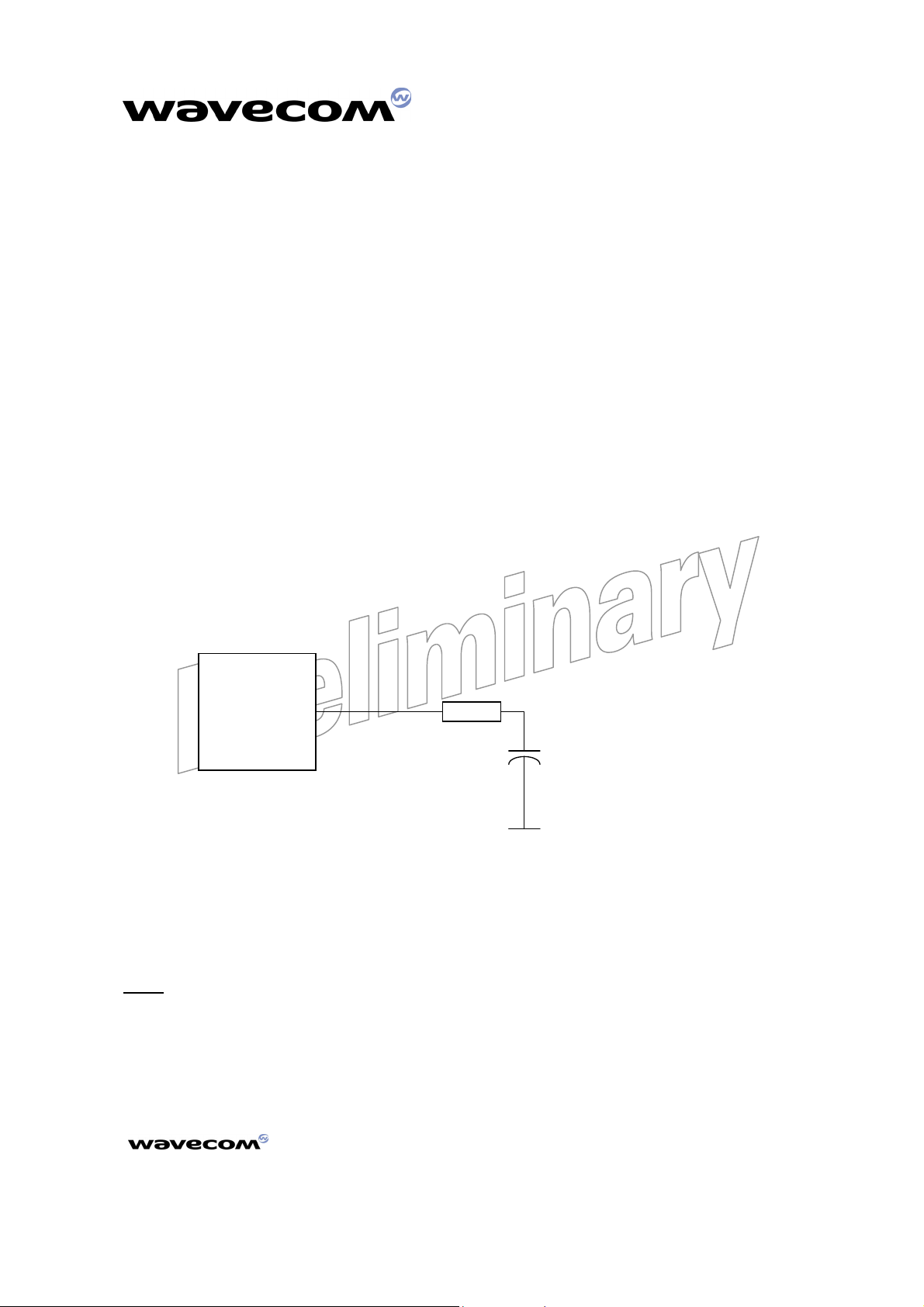
3.1.2.2 Typical application electrical diagram
3.1.2.2.1 Super Capacitor
470
WISMO
VCC_RTC
Ω
Q2501
+
Ex: EECEOEL474S
(Panasonic)
GND
Figure 3: RTC supplied by a super capacitor
Estimated range with 0.47 Farad Gold Cap: 25 minutes min.
: the Gold Capacitor maximum voltage is 2.5 V.
Note
confidential ©
This document is the sole and exclusive property of WAVECOM. Not to be distributed or divulged
without prior written agreement.
Ce document est la propriété exclusive de WAVECOM. Il ne peut être communiqué ou divulgué à
des tiers sans son autorisation préalable.
Page: 20 / 79
WM_PRJ_Q2501_PTS_002 - 001
March 2004
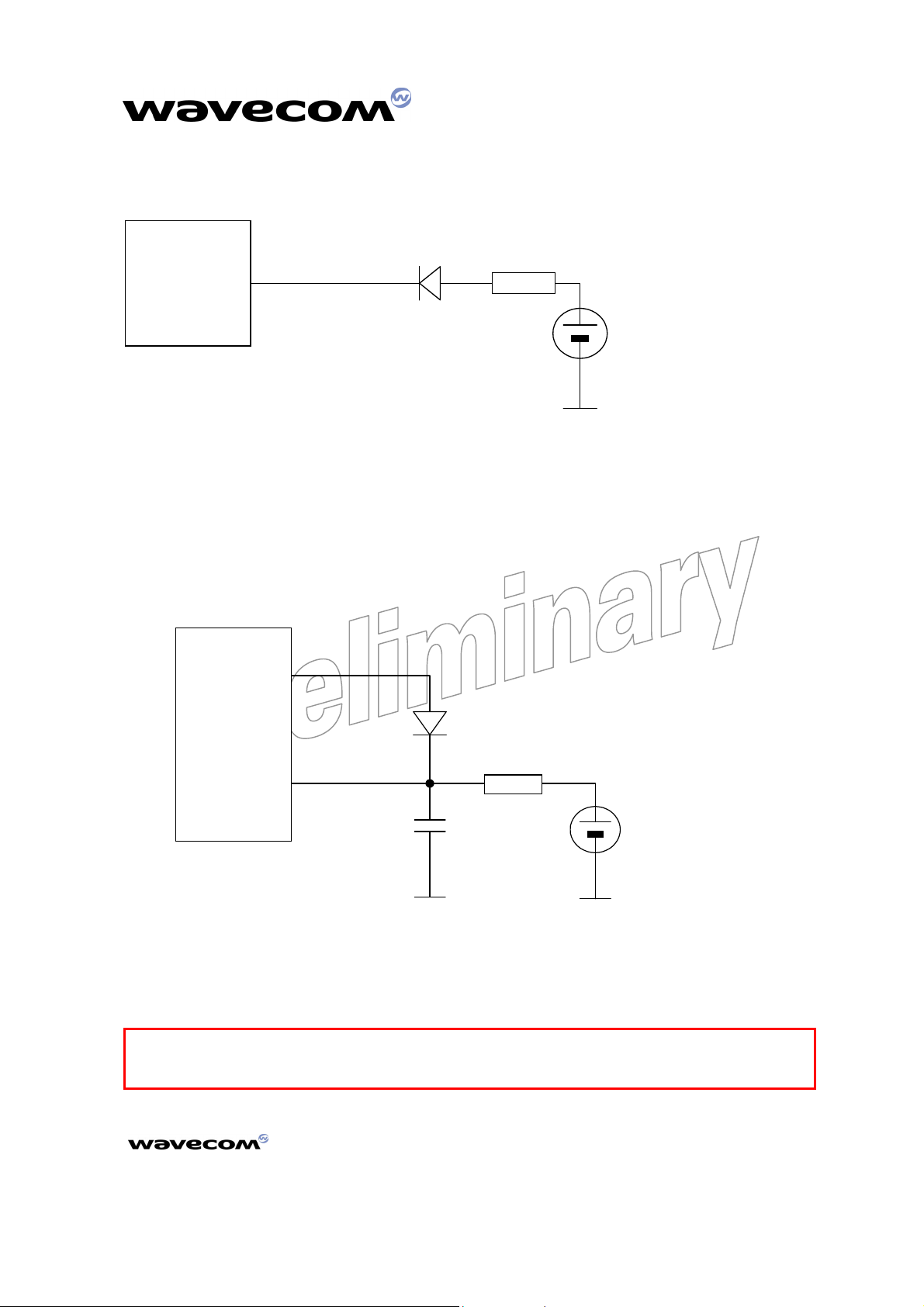
3.1.2.2.2 Non Rechargeable battery
10
WISMO
VCC_RTC
1
3
Ω
Q2501
BAS16
Figure 4: RTC supplied by a non rechargeable battery
Estimated range with 85 mAh battery: 800 h min.
Ex: Varta CR2016
GND
3.1.2.2.3 Rechargeable battery cell
VCC
1
WISMO
Q2501
VCC_RTC
2.2 µF
GND
BAS40
3
2.2 k
Ω
Ex: ML621
GND
Figure 5: RTC supplied by a rechargeable battery cell
Estimated range with 2 mAh rechargeable battery: ~15 hours.
Warning:
Before battery cell assembly insure that cell voltage is lower than 2.75 V to
avoid any damage to the WISMO module.
confidential ©
This document is the sole and exclusive property of WAVECOM. Not to be distributed or divulged
without prior written agreement.
Ce document est la propriété exclusive de WAVECOM. Il ne peut être communiqué ou divulgué à
des tiers sans son autorisation préalable.
Page: 21 / 79
WM_PRJ_Q2501_PTS_002 - 001
March 2004
3.2 Common GSM/GPS part
3.2.1 Module activation function (ON/~OFF)
The ON/~OFF input (pin 26) is used to switch ON (ON/~OFF=1) or OFF
(ON/~OFF=0) the WISMO Quik Q2501 module.
A high level signal has to be provided on the pin ON/~OFF to swith ON the
module.
The level of the voltage of this signal has to be maintained between 2.4 V and
VBATT during a minimum of 500 ms.
This signal can be left at high level until switch OFF.
SW500
1
VBATT
3
Figure 6: Example of ON/~OFF pin connection
2
ON/~OFF
3.2.2 Alternative download control function (BOOT)
If the standard X-modem download procedure does not work correctly, an
alternative download procedure can be selected with the BOOT input (pin 32).
This alternative download procedure requires a specific downloading software
tool.
The alternative download procedure is started when the BOOT pin is low
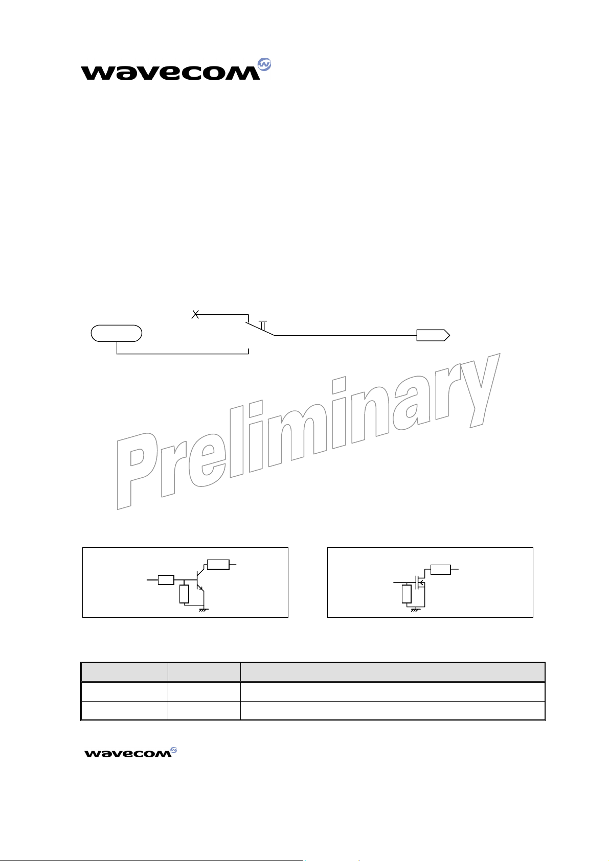
during the reset of the module. A low level of BOOT input has to be set
through a 1 kΩ resistor.
If used, this input has to be driven by an open collector or an open drain output
as shown in the diagram hereunder:
1 k
Ω
Switch BOOT
BOOT pin
OR
Switch BOOT
1 k
Ω
BOOT pin
Figure 7: Example of BOOT pin connection
Switch BOOT BOOT pin Operating mode
1 0 Alternative download mode (use of BOOT input)
0 1 Normal download mode (use of X-modem protocol)
confidential ©
This document is the sole and exclusive property of WAVECOM. Not to be distributed or divulged
without prior written agreement.
Ce document est la propriété exclusive de WAVECOM. Il ne peut être communiqué ou divulgué à
des tiers sans son autorisation préalable.
Page: 22 / 79

WM_PRJ_Q2501_PTS_002 - 001
March 2004
3.2.3 Reset function (~RST)
The ~RST input (pin 34) is used to force a reset procedure by providing low
level during at least 500 µs.
This signal has to be considered as an emergency reset only: a reset procedure
is automatically driven by an internal hardware during the power-up sequence.
This signal can also be used to provide a reset to an external device (it then
behaves as an output).
If no external reset is necessary this input can be left open.
If used (emergency reset), it has to be driven by an open collector or an open
drain output (due to the 4.7 kΩ internal pull-up resistor embedded into the
module) as shown in the diagram hereunder.
~RST: Pin 34
Switch RESET
Figure 8: Example of ~RST pin connection
Switch RESET ~RST pin Operating mode
1 0 Reset activated
0 1 Reset inactive
confidential ©
This document is the sole and exclusive property of WAVECOM. Not to be distributed or divulged
without prior written agreement.
Ce document est la propriété exclusive de WAVECOM. Il ne peut être communiqué ou divulgué à
des tiers sans son autorisation préalable.
Page: 23 / 79

WM_PRJ_Q2501_PTS_002 - 001
March 2004
3.2.4 Activity status indication function (FLASH_LED & GPS_TIMEPULSE)
The GSM and GPS activity status indication signals (FLASH_LED pin 72 and
GPS_TIMEPULSE pin 17) can be used to drive two LEDs through an opencollector digital transistor according to the module activity status.
« GSM »
1
2
Ω
Ω
D700
« GPS »
2
D702
1
VBATT
VBATT
FLASH_LED
GPS_TIMEPULSE
GND
GND
U700
1
2
U700
4
5
6
3
R700
470
R702
470
Figure 9: Example N°1 of GSM and GPS activity status implementation
In addition, given the electrical characteristics of the FLASH_LED output signal
(CMOS 2.8 V), it is possible to directly connect a LED and a resistor between
this output and VBATT to avoid adding a digital transistor inverter.
470
12
Ω
FLASH_LED
GND
Figure 10: Example N°2 of GSM activity status implementation
confidential ©
This document is the sole and exclusive property of WAVECOM. Not to be distributed or divulged
without prior written agreement.
Ce document est la propriété exclusive de WAVECOM. Il ne peut être communiqué ou divulgué à
des tiers sans son autorisation préalable.
Page: 24 / 79
 Loading...