

Page 1

WISMO Quik Q2400 series
Q2406 and Q2426
Customer Design Guidelines
Revision: 007
Date: January 2006
Page 2

WISMO Quik Q2400 series
Q2406 and Q2426
Customer Design Guidelines
Reference: WM_PRJ_Q2400_PTS_005
Revision: 007
Date: 18
th
January 2006
Confidential©
This document is the sole and exclusive property of WAVECOM. Not to be distributed or divulged
without prior written agreement.
All rights reserved
Page: 1 / 51
Page 3

WM_PRJ_Q2400_PTS_005 -007
18th January 2006
Document Information
Revision Date History of the evolution
001 14 Apr 03 Creation from PTS WM_PRJ_Q2400_PTS_002-002
002 13 Dec 04 Update document legal mentions.
003 26 Feb 05 Add SIM 1.8/3V management
004 26 Feb 05 No content modification; document goes from version 3 to
005 4 March 05 No content modification; document goes from version 4 to
006 25th July
2005
007 18th January
2006
Remove Q2406D and Q2426D of available products list.
Update Power Supply section
Modification of RF connection mode
Modification of figures and mechanical information due to
change of module design
Update of 3V SIM Socket implementation diagram
version 4
version 5
Update §2.1.3.2, §3.2.2, §4 for Lead free introduction(
Update §1.1.1.3 for power supply voltage
Update §1.1.1.4 for module capability
Update §2.2.2.2 for two-wire interface
Update §2.2.1 for serial resistors on digital I/O
Update §2.2.5 for Uart Input level in OFF state and serial
resistors
Update §2.2.6.1 for SIM_VCC capacitor
Update §2.4 for battery type charging and software version
Confidential©
All rights reserved
Page: 2 / 51
This document is the sole and exclusive property of WAVECOM. Not to be
distributed or divulged without prior written agreement.
Page 4

WM_PRJ_Q2400_PTS_005 -007
AAA
18th January 2006
Overview
This document gives recommendations for WISMO Quik Q24x6 sub-series
integration in an application and particularly:
• The baseband design rules and typical implementation examples,
• The RF design rules and typical implementation examples
• The mechanical constraints for module fitting,
• The PCB routing recommendations,
• The Test and download recommendations.
It also gives some part references and suppliers.
8 versions of the WISMO Quik Q24x6 sub-series are available:
• Q2406A: E-GSM/GPRS 900/1800 MHz version with 16 Mbits of Flash
memory and 2 Mbits of SRAM (16/2).
• Q2406B: E-GSM/GPRS 900/1800 MHz version with 32 Mbits of Flash
memory and 4 Mbits of SRAM (32/4).
• Q2426A: GSM/GPRS 850/1900 MHz version with 16 Mbits of Flash
memory and 2 Mbits of SRAM (16/2).
• Q2426B: GSM/GPRS 850/1900 MHz version with 32 Mbits of Flash
memory and 4 Mbits of SRAM (32/4).
Please be aware that some of the interfaces provided by the Q24x6 sub-series
can not be handled when using the module driven by AT commands.
TTT
These functions have then to be managed externally i.e using the main
processor of the application.
This symbol is used to indicate the interfaces not available with AT
commands.
Confidential©
All rights reserved
Page: 3 / 51
This document is the sole and exclusive property of WAVECOM. Not to be
distributed or divulged without prior written agreement.
Page 5

WM_PRJ_Q2400_PTS_005 -007
18th January 2006
Contents
Document Information........................................................................... 2
Overview................................................................................................ 3
Contents................................................................................................ 4
List of Figures........................................................................................ 6
Caution.................................................................................................. 7
Trademarks ........................................................................................... 7
Reference documents ............................................................................ 8
1 General description......................................................................... 9
1.1 General information .................................................................................. 9
1.1.1 Module Features ............................................................................... 9
1.1.2 Module external connection .............................................................. 9
1.1.3 Additional customizing functions .................................................... 10
1.1.4 RoHS compliance............................................................................ 10
2 Baseband Design........................................................................... 11
2.1 Power supply and ground design rules................................................... 11
2.1.1 Electrical constraints ....................................................................... 11
2.1.2 Design Requirements...................................................................... 13
2.1.3 PCB routing constraints .................................................................. 15
2.2 Digital I/O and peripheral implementation ............................................... 16
2.2.1 Electrical information for digital I/O ................................................. 16
2.2.2 LCD interface .................................................................................. 16
2.2.3 SPI Auxiliary bus............................................................................. 17
2.2.4 Keyboard interface .......................................................................... 17
2.2.5 Main serial link (UART1).................................................................. 18
2.2.6 SIM interface .................................................................................. 20
2.3 Analog I/O implementation ..................................................................... 24
2.3.1 Analog to Digital Converter (ADC) inputs ........................................ 24
2.3.2 Audio interface................................................................................ 25
2.4 Battery charging interface....................................................................... 31
2.5 ON / ~OFF .............................................................................................. 32
2.6 BOOT signal (optional) ............................................................................ 33
Confidential©
All rights reserved
Page: 4 / 51
This document is the sole and exclusive property of WAVECOM. Not to be
distributed or divulged without prior written agreement.
Page 6

WM_PRJ_Q2400_PTS_005 -007
18th January 2006
Reset signal (~RST) ................................................................................ 34
2.7
2.8 External Interrupt (~INTR)....................................................................... 34
2.9 VCC output ............................................................................................. 35
2.10 VCC_RTC (Real Time Clock Supply) ......................................................... 35
2.10.1 General ........................................................................................... 35
2.10.2 Typical implementation................................................................... 36
3 Radio design ................................................................................. 38
3.1 Antenna characteristics .......................................................................... 38
3.2 Antenna implementation ........................................................................ 38
3.2.1 Recommendations .......................................................................... 38
3.2.2 RF connection ................................................................................. 39
4 Mechanical specifications............................................................. 41
5 PCB design.................................................................................... 42
5.1 General design rules ............................................................................... 42
5.2 Design rules for application manufacturing............................................. 42
5.3 Recommendation for lead free soldering........................................... 42
5.4 Power supply.......................................................................................... 42
5.5 Pads design ............................................................................................ 43
6 EMC recommendations ................................................................. 44
7 Firmware upgrade ......................................................................... 45
7.1 Recommendations .................................................................................. 45
7.2 Nominal upgrade procedure.................................................................... 45
7.3 Backup procedure ................................................................................... 46
8 Embedded testability .................................................................... 47
9 Part references and suppliers........................................................ 50
9.1 General Purpose Connector .................................................................... 50
9.2 SIM Card Reader .................................................................................... 50
9.3 Microphone ............................................................................................ 50
9.4 Speaker .................................................................................................. 51
9.5 Antenna Cable ........................................................................................ 51
9.6 GSM antenna ......................................................................................... 51
Confidential©
All rights reserved
Page: 5 / 51
This document is the sole and exclusive property of WAVECOM. Not to be
distributed or divulged without prior written agreement.
Page 7

WM_PRJ_Q2400_PTS_005 -007
18th January 2006
List of Figures
Figure 1: Typical power supply voltage in GSM mode ...................................... 11
Figure 2: Maximal voltage ripple (Uripp) vs Frequency in GSM & DCS ............. 13
Figure 3: Burst simulation circuit ...................................................................... 14
Figure 4: Example of SPI Bus typical implementation ....................................... 17
Figure 5: Example of keyboard implementation................................................. 18
Figure 6: Example of RS232 level shifter implementation.................................. 19
Figure 7: Example of Serial Link interface implementation ................................ 19
Figure 8 Example of 3V SIM Socket implementation ......................................... 21
Figure 9: Example of 1.8 V / 3 V SIM interface implementation......................... 22
Figure 10: Example of 3 V / 5 V SIM interface implementation.......................... 23
Figure 11: Example of ADC input implementation............................................. 24
Figure 12: Microphone decoupling capacitor .................................................... 25
Figure 13: Example of main microphone MIC2 implementation (differential
connection) ................................................................................................. 26
Figure 14: MIC1 inputs (differential connection) ............................................... 27
Figure 15: MIC1 inputs (single-ended connection)............................................ 28
Figure 16: Speaker outputs (differential mode).................................................. 29
Figure 17: Speaker outputs (single-ended connection)...................................... 29
Figure 18: Example of Buzzer implementation .................................................. 30
Figure 19: Example of battery implementation.................................................. 31
Figure 20: BOOT pin connection....................................................................... 33
Figure 21: ∼RST pin connection ........................................................................ 34
Figure 22: RTC Supplied by a capacitor ............................................................ 36
Figure 23: RTC supplied by a super capacitor ................................................... 36
Figure 24: RTC supplied by a battery cell with regulator................................... 37
Figure 25: RTC supplied by a non rechargeable battery .................................... 37
Figure 26: Antenna connection......................................................................... 39
Figure 27: Antenna cable preparation (drawing not to scale) ............................ 40
Figure 28: Maximum bulk occupied on the application board ........................... 41
Figure 29: Pads design ..................................................................................... 43
Figure 30: Example of serial link routing for downloading................................. 47
Figure 31: Download cable schematics (1/2)..................................................... 48
Figure 32: Download cable schematics (2/2)..................................................... 49
Confidential©
All rights reserved
Page: 6 / 51
This document is the sole and exclusive property of WAVECOM. Not to be
distributed or divulged without prior written agreement.
Page 8

WM_PRJ_Q2400_PTS_005 -007
18th January 2006
Caution
Information furnished herein by Wavecom are accurate and reliable. However no
responsibility is assumed for its use. Please read carefully the safety precautions
for a terminal based on WISMO Quik Q24x6 Series.
General information about Wavecom and its range of products is available at the
following internet address: http://www.wavecom.com
Trademarks
®, WAVECOM®, WISMO®, , Open AT® and certain other trademarks and logos
appearing on this document, are filed or registered trademarks of Wavecom S.A.
in France or in other countries. All other company and/or product names
mentioned may be filed or registered trademarks of their respective owners.
Confidential©
This document is the sole and exclusive property of WAVECOM. Not to be
distributed or divulged without prior written agreement.
All rights reserved
Page: 7 / 51
Page 9

WM_PRJ_Q2400_PTS_005 -007
18th January 2006
Reference documents
[1] WISMO Quik Q2406 and q2426 Product Specification
WM_PRJ_Q2400_PTS_002
[2] WISMO Quik Q2400 Series Process Customer Guidelines
WM_PRJ_Q2400_PTS_006
[3] AT Commands Interface Guide
WM_ASW_OAT_UGD_00016
Confidential©
All rights reserved
Page: 8 / 51
This document is the sole and exclusive property of WAVECOM. Not to be
distributed or divulged without prior written agreement.
Page 10

WM_PRJ_Q2400_PTS_005 -007
18th January 2006
1 General description
1.1 General information
1.1.1 Module Features
WISMO Quik Q24x6 sub-series is a range of self-contained E-GSM
900/1800 or 850/1900 dual-band modules including the following features:
1.1.1.1 Overall dimensions
• 58.4 x 32.2 x 3.9 mm.
1.1.1.2 Power consumption
• 2 Watts E-GSM 900/GSM 850 radio section running under 3.6 Volts.
• 1 Watt GSM1800/1900 radio section running under 3.6 Volts.
1.1.1.3 Power supply voltage
• Digital section running under 2.8 Volts.
• 3V only SIM interface (for both 1.8 V and 5 V SIM interface with
external adaptation, refer to § 0 and 2.2.6.3 ).
1.1.1.4 Module capability
• Real Time Clock with calendar.
• Battery charge management.
• Echo Cancellation + noise reduction.
• Full GSM or GSM/GPRS software stack.
• Complete shielding.
• Complete interfacing through a 60-pin connector:
o Power supply,
o Serial link,
o Audio,
o SIM card interface,
o Keyboard,
o LCD.
1.1.2 Module external connection
WISMO Quik Q24x6 sub-series has two external connections:
• RF connection pads (to the antenna),
• 60-pin General Purpose Connector (GPC) to Digital, Keyboard, Audio
and Supply.
Confidential©
All rights reserved
Page: 9 / 51
This document is the sole and exclusive property of WAVECOM. Not to be
distributed or divulged without prior written agreement.
Page 11

WM_PRJ_Q2400_PTS_005 -007
18th January 2006
1.1.3 Additional customizing functions
WISMO Quik Q24x6 sub-series is designed to fit in very small terminals
and only some custom functions have to be added to make a complete
dual-band solution:
• Keypad and LCD module,
• Earpiece and Microphone,
• Base connector,
• Battery,
• Antenna,
• SIM connector.
1.1.4 RoHS compliance
The WISMO Quik Q24x6 sub-series is now compliant with RoHS
(Restriction of Hazardous Substances in Electrical and Electronic
Equipment) Directive 2002/95/EC which sets limits for the use of certain
restricted hazardous substances. This directive states that “from 1st July
2006, new electrical and electronic equipment put on the market does not
contain lead, mercury, cadmium, hexavalent chromium, polybrominated
biphenyls (PBB) or polybrominated diphenyl ethers (PBDE)”.
Modules which are compliant with this directive are
identified by the RoHS logo on their label.
Confidential©
All rights reserved
Page: 10 / 51
This document is the sole and exclusive property of WAVECOM. Not to be
distributed or divulged without prior written agreement.
Page 12
WM_PRJ_Q2400_PTS_005 -007
18th January 2006
2 Baseband Design
Note:
Some of the WISMO interface signals are multiplexed in order to limit number of
pins but this architecture implies some limitation.
For example in case of using SPI bus, 2-wire bus can not be used.
Warning:
All external signals must be inactive when the WISMO module is OFF to avoid
any damage when starting and allow WISMO module to start correctly.
2.1 Power supply and ground design rules
2.1.1 Electrical constraints
The power supply is one of the key issues in the design of a GSM terminal. Due
to the bursted emission in GSM / GPRS, the power supply must be able to
deliver high current peaks in a short time and assured that the voltage delivered
to the module remains always under the limits specified in the table “Maximum
voltage ripple (Uripp) vs Frequency in GSM & DCS” hereafter, specially during
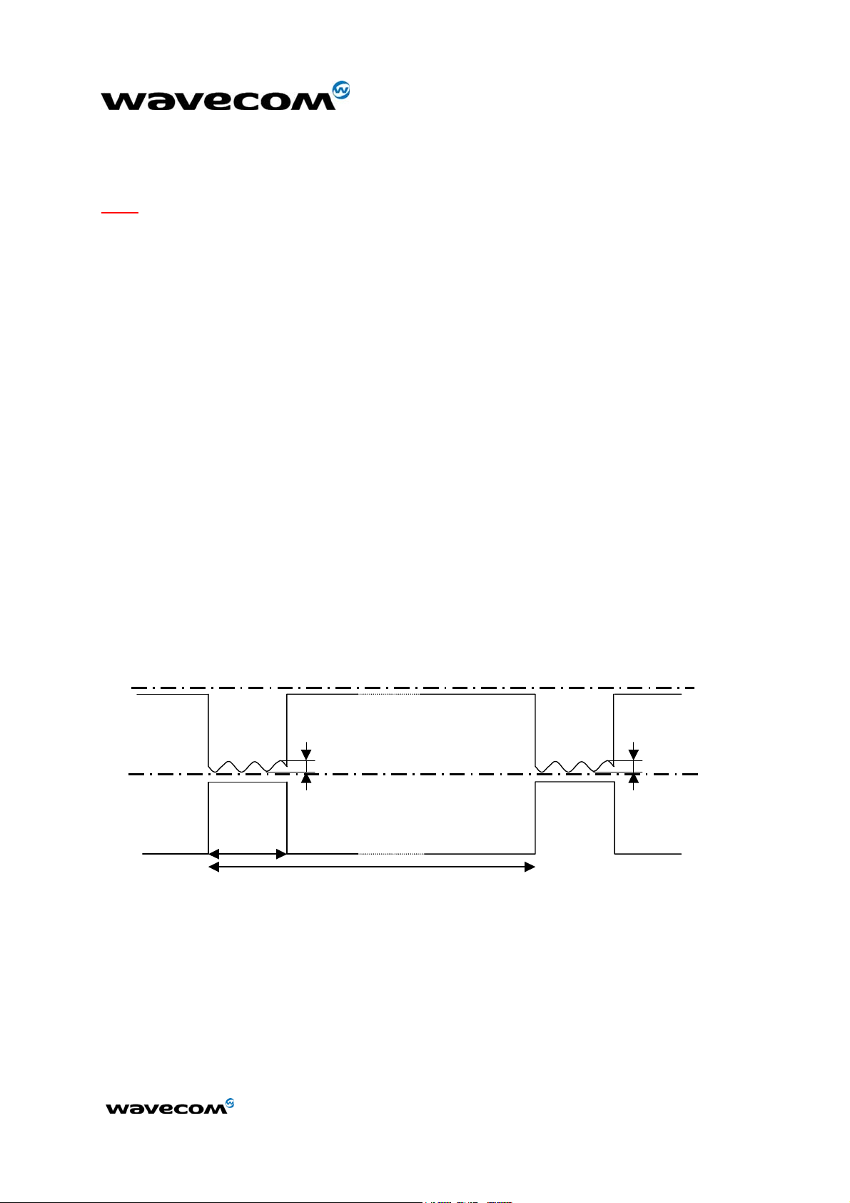
burst while there is a drop of voltage (see Figure 1).
In communication mode, a GSM/GPRS class 2 terminal emits 577 µs radio bursts
every 4.615 ms.
In communication mode, a GPRS class 10 terminal emits 1154 µs radio bursts
every 4.615 ms.
VBATT
IBATT
(1)
or VDD if connected to VBATT
(1)
t = 577 µs
Uripp
T = 4.615 ms
Uripp
Vmax
Vmin
Figure 1: Typical power supply voltage in GSM mode
Two different inputs are provided for the power supply:
• the first one, VBATT is used to supply the RF part,
• the second one, VDD is used to supply the baseband part.
The power supply voltage features given in the table hereafter will guarantee
nominal functioning of the module.
Confidential©
All rights reserved
Page: 11 / 51
This document is the sole and exclusive property of WAVECOM. Not to be
distributed or divulged without prior written agreement.
Page 13
WM_PRJ_Q2400_PTS_005 -007
18th January 2006
Power Supply Voltage
V
V
MIN
V
NOM
MAX
VBATT 3.3 V (*) 3.6 V 4.5 V (**)
VDD 3.1 V 4.5 V
Table 1: Power supply voltage
(*): This value has to be guaranteed during the burst (with 2.0 A Peak in GSM or
GPRS mode).
(**): max operating Voltage Stationary Wave Ratio (VSWR) 2:1.
When the module is supplied with a battery, the total impedance
(battery+contacts+protections+PCB) should be < 150 mΩ to limit voltage dropout within emission burst.
As the radio power amplifier is directly connected to VBATT, the module is
sensitive to any Alternative Current on lines. When a DC/DC converter is used,
Wavecom recommends to set the converter frequency in such a way that the
resulting voltage does not exceed the values in following table and Figure 2.
Freq.
(kHz)
U
Max
ripp
(mVpp)
Freq.
(kHz)
U
Max
ripp
(mVpp)
Freq.
(kHz)
U
Max
ripp
(mVpp)
<100 50 800 4 1500 34
200 15.5 900 15.2 1600 33
300 6.8 1000 9.5 1700 37
400 3.9 1100 32 1800 40
500 4 1200 22 >1900 40
600 2 1300 29
700 8.2 1400 30
Table 2: Maximum voltage ripple (Uripp) vs Frequency in GSM & DCS
Confidential©
All rights reserved
Page: 12 / 51
This document is the sole and exclusive property of WAVECOM. Not to be
distributed or divulged without prior written agreement.
Page 14

WM_PRJ_Q2400_PTS_005 -007
18th January 2006
50
45
40
35
30
25
20
Uripp (mVpp)
15
10
5
0
200 400 600 800 1000 1200 1400 1600 1800
Input Frequency (kHz)
for f<100kHz U
for f> 1800kHz U
Max = 50mVpp
ripp
Max = 40 mVpp
ripp
Figure 2: Maximal voltage ripple (Uripp) vs Frequency in GSM & DCS
2.1.2 Design Requirements
2.1.2.1 Risk
VBATT supplies directly the RF components with 3.6 V. It is essential to keep a
minimum voltage ripple at this connection in order to avoid any phase error.
Insufficient power supply voltage could dramatically affect some RF
performances:
• TX power of course and modulation spectrum,
• EMC performances (spurious emission),
• Emissions spectrum,
• Phase error and frequency error.
2.1.2.2 General design rules
A careful attention should be paid to:
• Quality of the power supply: capacity to deliver high peak current in a
short time (bursted radio emission), low ripple and low impedance.
• The battery charger line must support 800 mA to comply with the voltage
level required for the product.
• The VBATT lines on the PCB must support peak currents with a voltage
drop below the specified limit.
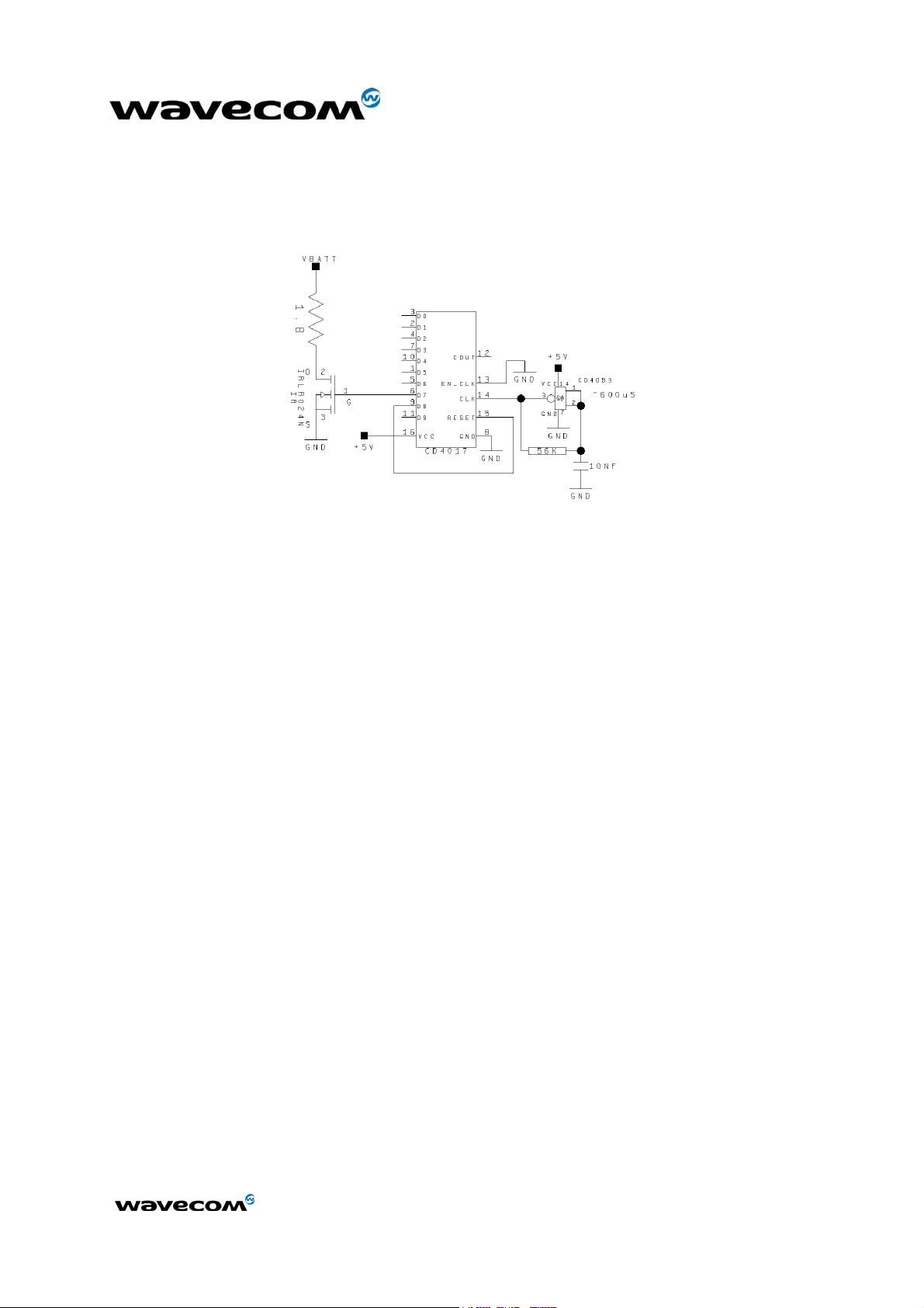
In order to test the supply tracks, a burst simulation circuit is shown hereafter.
This circuit simulates burst emissions, equivalent to bursts generated when
transmitting at full power.
Confidential©
All rights reserved
Page: 13 / 51
This document is the sole and exclusive property of WAVECOM. Not to be
distributed or divulged without prior written agreement.
Page 15
WM_PRJ_Q2400_PTS_005 -007
18th January 2006
Warning:
Attention must be paid to the power supply capacity when replacing a
WISMO Quik Q2403 module, on an existing application, by a Q24x6 module as
this last one is more demanding due to GPRS class 10.
Figure 3: Burst simulation circuit
2.1.2.3 Battery for handset integration
In a handset application, the WISMO Quik Q24x6 sub-series may be directly
connected to a Li-Ion battery (3.7 V typical voltage, with internal PCM –
Protection Circuit Module). The internal impedance of the battery must be lower
than 150 mΩ to limit voltage drop-out within emission burst (max. drop 0.3 V @
2W).
Battery internal impedance must take into account:
the internal impedance of the battery cell,
the protection circuit impedance,
the “packaging” impedance (contacts),
the PCB track impedance up to the WISMO module pin.
2.1.2.4 External DC power supply for vertical application
In a vertical application, the WISMO Quik Q24x6 sub-series may be connected to
DC power supply directly or via a DC/DC converter on the mother board. The
internal impedance of the power supply must be lower than 150 mΩ to limit
voltage drop-out within emission burst (max. drop 0.3 V @ 2W).
This impedance must take into account:
the internal impedance of the power supply,
the protection circuit impedance,
the “packaging” impedance (contacts),
the PCB track impedance up to the WISMO module pin.
Confidential©
All rights reserved
Page: 14 / 51
This document is the sole and exclusive property of WAVECOM. Not to be
distributed or divulged without prior written agreement.
Page 16

WM_PRJ_Q2400_PTS_005 -007
18th January 2006
Linear regulation (recommended) or PWM (Pulse Width Modulation) converter
(usable) are preferred for low noise.
PFM (Power Frequency Modulation) or PSM (Phase Shift Modulation) systems
must be avoided.
2.1.3 PCB routing constraints
2.1.3.1 Power supply routing Constraints
• A ground plane must be provided on the PCB. This plane must not be
parcelled out.
• Attention shall be paid to the power supply tracks and to the ground plane
which supply the module. The tracks and the plane used must support
current peaks.
• Since the maximum peak current can reach 2 A, Wavecom strongly
recommends a large width for the layout of the power supply signal (to
avoid voltage loss between the external power supply and the module
supply. Filtering capacitors, near the module power supply, could also be
added (refer to section 2.1.3.3).
• The routing must be done in such a way that the total impedance line
must be ≤ 10 mΩ @ 217 Hz. This impedance must include the via
impedances.
• Same care shall be taken when routing the ground supply.
• If these design rules are not followed, phase error (peak) and power loss
could occur.
2.1.3.2 Application ground plane and shielding connection
The grounding connection is done through the shielding the four legs have to
be soldered to the ground plane (
soldering in Section 5.3)
.
see Wavecom recommendation for lead free
A ground plane must be available on the application board to provide efficient
connection to the WISMO module shielding.
Best shielding performance will be achieved if the application ground plane is a
complete layer of the application PCB:
• To ensure a good shielding of the module, a complete ground plane layer
must be available, with no trade-off. Connections between other ground
planes shall be done with vias.
• Without this ground plane, external Tx spurious or Rx blockings could
appear.
It is strongly recommended to avoid routing any signals under the module.
Confidential©
All rights reserved
Page: 15 / 51
This document is the sole and exclusive property of WAVECOM. Not to be
distributed or divulged without prior written agreement.
Page 17

WM_PRJ_Q2400_PTS_005 -007
18th January 2006
2.1.3.3 Decoupling of power supply signals
Decoupling capacitors on VBATT and VDD lines are imbedded in the module. So
it should not be necessary to add decoupling capacitors close to the module.
However, in case of EMI/RFI problem, some signals like VBATT and charge line
(CHG_IN) may require some EMI/RFI decoupling: parallel 33 pF capacitor close to
the module or a serial ferrite bead (or both to get better results).
In case a ferrite bead is used, the recommendation given for the power supply
connection must be carefully followed (high current capacity and low
impedance).
2.2 Digital I/O and peripheral implementation
2.2.1 Electrical information for digital I/O
All digital I/O comply with 3Volts CMOS.
To interface the WISMO Quik Q24x6 sub-series digital signals with other logics:
• 3.3 V logic: some serial resistors (more than 11kΩ) can be added on the
lines,
• For higher voltage logics, a resistor bridge or a level shifter IC can be
added.
2.2.2 LCD interface
The WISMO Quik Q24x6 sub-series can be connected to a LCD module driver
through either a SPI bus or a two-wire interface.
2.2.2.1 SPI bus
The SPI bus includes a CLK signal (SPI_CLK), an I/O signal (SPI_IO) and an EN
signal (SPI_EN) complying with SPI bus standard.
Confidential©
All rights reserved
Page: 16 / 51
This document is the sole and exclusive property of WAVECOM. Not to be
distributed or divulged without prior written agreement.
Page 18

A
Typical implementation:
WM_PRJ_Q2400_PTS_005 -007
18th January 2006
VCC
VCC
SPI_IO
SPI_CLK
GPO or GPIO
SPI_EN
RST
Figure 4: Example of SPI Bus typical implementation
T
T
2.2.2.2 Two-wire interface
The two-wire interface includes a CLK signal (SCL) and a DATA signal (SDA)
T
complying with a standard 96 kHz interface. The maximum speed transfer is
400 kbits/s.
Note:
The two-wire interface is reserved for future use. A software emulated
version of this interface using GPIOs is available. See “AT Command Interface
Guide” [3] for more information.
2.2.3 SPI Auxiliary bus
A second SPI Chip Enable (called SPI_AUX) can be used to add a SPI peripheral
to the WISMO Quik Q24x6 sub-series.
2.2.4 Keyboard interface
This interface provides 10 connections:
• 5 rows (ROW0 to ROW4),
• 5 columns (COL0 to COL4).
The scanning is a digital one, and the debouncing is done in the WISMO
module. No discrete components like R, C (Resistor, Capacitor) are needed.
Confidential©
All rights reserved
Page: 17 / 51
This document is the sole and exclusive property of WAVECOM. Not to be
distributed or divulged without prior written agreement.
Page 19

Typical Implementation
Figure 5: Example of keyboard implementation
WM_PRJ_Q2400_PTS_005 -007
18th January 2006
:
2.2.5 Main serial link (UART1)
A flexible 6-wire serial interface is available complying with V24 protocol
signaling but not with V28 (electrical interface) due to a 2.8 Volts interface.
The signals are:
• TX data input (CT103/TX),
• RX data output (CT104/RX),
• Request To Send input (CT105/RTS),
• Clear To Send output (CT106/CTS),
• Data Terminal Ready input (CT108-2/DTR),
• Data Set Ready output (CT107/DSR).
Note
: the WISMO Quik Q24x6 module is a DCE (Data Communication
Equipment).
The Q24x6 sub-series has been designed to allow a certain flexibility in the use
of the serial interface signals. However, the use of TX, RX, CTS and RTS signals
is mandatory which is not the case for DTR, DSR, DCD and RI signals which can
be left disconnected if not used.
In particular, it is necessary to use RTS and CTS for hardware flow control in
order to avoid data corruption during transmission.
The rising time and falling time of the reception signals (mainly CT103) have to
be less than 200 ns.
The 2 additional signals are Data Carrier Detect (CT109/DCD) and Ring Indicator
(CT125/RI).
Confidential©
All rights reserved
Page: 18 / 51
This document is the sole and exclusive property of WAVECOM. Not to be
distributed or divulged without prior written agreement.
Page 20

WM_PRJ_Q2400_PTS_005 -007
18th January 2006
To enable the module to switch OFF correctly, the level shifter outputs (module
side) or host processor outputs must be set at low level (0V) or in high
impedance.
Typical implementation with a terminal
:
DCE DTE
VCC
R
Figure 6: Example of RS232 level shifter implementation
Typical implementation with a microprocessor:
+3V
+3V
+3V
The figure above shows a typical implementation when the WISMO Quik Q24x6
module is connected to a host microprocessor which is 2.8 V tolerant on the
serial port signals.
Host Microprocessor
Figure 7: Example of Serial Link interface implementation
Confidential©
All rights reserved
Page: 19 / 51
This document is the sole and exclusive property of WAVECOM. Not to be
distributed or divulged without prior written agreement.
Page 21

WM_PRJ_Q2400_PTS_005 -007
18th January 2006
Typical serial resistors values (R) for signals between application and WISMO
Quik Q2400 (mainly CT103/TX) (see Figure 6).
UART baud rate
Host output voltage
<3.1V 3.2V 3.3V
9 600
19 200
38 400
57 600
115 200
R < 62 kΩ 6.8 kΩ< R < 62 kΩ 11 kΩ< R < 62 kΩ
R < 30 kΩ 6.8 kΩ< R < 30 kΩ 11 kΩ< R < 30 kΩ
R < 15 kΩ 6.8 kΩ< R < 15 kΩ 11 kΩ< R < 15 kΩ
R < 10 kΩ 6.8 kΩ< R < 10 kΩ
R < 5.1 kΩ
Not supported Not supported
Not supported
The minimal value is determined to limit the current in the input pin of the
Module and the maximal value is determined by its input capacitance. That
explains why some combinations speed / voltage are incompatible.
2.2.6 SIM interface
2.2.6.1 SIM 3V management
The SIM interface controls a 3 V SIM card only.
Nevertheless, it is possible to manage 1.8V/3V or 3V/5V SIM cards using an
external voltage level shifter controlled by the GPO0 output signal (refer to §
2.2.6.2 and § 2.2.6.3).
It is recommended to add Transient Voltage Suppressor diodes (TVS) on the
signal connected to the SIM socket in order to prevent any Electrostatic
Discharge.
TVS diodes with low capacitance (less than 10 pF) have to be connected on
SIM_CLK and SIM_DATA signals to avoid any disturbance of the rising and
falling edge.
These types of diodes are mandatory for the Full Type Approval. They shall be
placed as close as possible to the SIM socket.
The following references can be used: DALC208SC6 from ST Microelectronics.
Confidential©
All rights reserved
Page: 20 / 51
This document is the sole and exclusive property of WAVECOM. Not to be
distributed or divulged without prior written agreement.
Page 22

WM_PRJ_Q2400_PTS_005 -007
A
Typical implementation with SIM detection:
18th January 2006
GND
(1)
GND
(2)
GND
(1) Recommended components: DALC208SC6 (SGS-THOMSON).
(2) Recommended components: ESDA6V1SC6 (ST).
Figure 8 Example of 3V SIM Socket implementation
SIM socket connection:
SIM socket pin description
Signal Pin number Description
VCC 1 SIM_VCC
C
100 nF
SIM_VCC 1
SIM_RST 2
SIM_CLK 3
VCC 4
SIM_DAT
SIM_PRES 8
470pf
GND
5
7
100
kΩ
VCC
RST
CLK
CC4
GND
VPP
I / O
CC8
RST 2 SIM_RST
CLK 3 SIM_CLK
CC4 4 VCC module
GND 5 GROUND
VPP 6 Not connected
I/O 7 SIM_DATA
CC8 8
SIM_PRES with 100 kΩ pull down resistor
The capacitance value on the SIM_VCC must not exceed 100nF.
It is possible to use a capacitor value greater than 100nF but less than 330nF on
SIM_VCC, if an additional capacitor with a minimum value of 27µF (ESR <100
mΩ, X5R ceramic) is placed between VCC output (pin 40) and the GND.
Confidential©
All rights reserved
Page: 21 / 51
This document is the sole and exclusive property of WAVECOM. Not to be
distributed or divulged without prior written agreement.
Page 23

WM_PRJ_Q2400_PTS_005 -007
18th January 2006
2.2.6.2 SIM 1.8 V / 3 V management
It is possible to manage 1.8 V and 3 V SIM cards using an external level shifter
device (see Figure below).
In this case, depending on the type of SIM detected, the module firmware
triggers the GPO0 output signal (pin #26) in order to properly set the external
SIM driver level (1.8 V or 3 V).
As for 3 V SIM, it is recommended to add Transient Voltage Suppressors on the
signals connected to the SIM socket (refer to Figure 9).
Typical implementation:
SIM_CLK
SIM_RST
SIM_DATA
VCC
GPO0
WISMO
SIM_VCC
Q2400
SIM_PRES
Truth
table:
M0
0V
0V
DVCC
DVCC
DVCC
M1
0V
DVCC
0V
0V
DVCC
VCC
2.8 V
LEVEL SHIFTER
1
CIN
2
RIN
3
DATA
4
DDRV
5
DVCC
6
M2
7
M1
8
M0
LTC1555L-1.8
DVCC = 2.8 V
M2
0V or DVCC
0V or DVCC
0V
DVCC
0V or DVCC
Operating Mode
Shutdown (VCC = 0V)
VCC = VIN
VCC = 3 V
VCC = 1.8 V
VCC = 5 V
CLK
RST
I/O
VCC
VIN
C1+
C1-
GND
16
15
14
13
12
11
10
VCC
2.8 V
SIM
1 Ω
to
4.7 Ω
1 µF
9
100 nF
3
2
7
1
6
4
VCC
8
100 kΩ
470 pF
5
Socket
CLK
RST
I/O
VCC = 1.8 V or 3 V
IVCC = 10 mA
2.2 µF
VPP
CC4
CC8
GND
Figure 9: Example of 1.8 V / 3 V SIM interface implementation
Confidential©
All rights reserved
Page: 22 / 51
This document is the sole and exclusive property of WAVECOM. Not to be
distributed or divulged without prior written agreement.
Page 24

WM_PRJ_Q2400_PTS_005 -007
18th January 2006
2.2.6.3 SIM 3 V / 5 V management
It is possible to manage 3 V and 5 V SIM cards using an external level shifter
device (see Figure below).
In this case, depending on the type of SIM detected, the module firmware
triggers the GPO0 output signal (pin #26) in order to properly set the external
SIM driver level (3 V or 5 V).
As for 3 V SIM, it is recommended to add Transient Voltage Suppressors on the
signals connected to the SIM socket (refer to Figure 10).
Typical implementation:
WISMO
Q2400
SIM_CLK
SIM_RST
SIM_DATA
VCC
GPO0
SIM_VCC
SIM_PRES
M0
0V
0V
DVCC
DVCC
DVCC
VCC
2.8 V
Truth
table:
M1
0V
DVCC
0V
0V
DVCC
LEVEL SHIFTER
1
CIN
2
RIN
3
DATA
4
DDRV
5
DVCC
6
M2
7
M1
8
M0
LTC1555L-1.8
DVCC = 2.8 V
M2
0V or DVCC
0V or DVCC
0V
DVCC
0V or DVCC
Operating Mode
Shutdown (VCC = 0V)
VCC = VIN
VCC = 3 V
VCC = 1.8 V
VCC = 5 V
CLK
RST
I/O
VCC
VIN
C1+
C1-
GND
16
15
14
13
12
11
10
VCC
2.8 V
SIM
1 Ω
to
4.7 Ω
1 µF
9
100 nF
3
2
7
1
6
4
VCC
8
100 kΩ
470 pF
5
Socket
CLK
RST
I/O
VCC = 3 V or 5 V
IVCC = 10 mA
2.2 µF
VPP
CC4
CC8
GND
Figure 10: Example of 3 V / 5 V SIM interface implementation
Confidential©
All rights reserved
Page: 23 / 51
This document is the sole and exclusive property of WAVECOM. Not to be
distributed or divulged without prior written agreement.
Page 25

WM_PRJ_Q2400_PTS_005 -007
18th January 2006
2.2.6.4 PCB constraints for SIM interface
• For the SIM interface, length of the track between the WISMO module and
the SIM connector should be as short as possible. Maximum length
recommended is 10 cm.
• ESD protection is mandatory on the SIM lines if access from outside of the
SIM connector is possible.
2.3 Analog I/O implementation
2.3.1 Analog to Digital Converter (ADC) inputs
Two Analog to Digital Converter are available on the WISMO Quik Q24x6 subseries:
The first one (AUXV0) is a general purpose converter,
The second one (BAT_TEMP) is used for battery temperature monitoring.
These converters have a 10-bit resolution, ranging from 0 to 2.8 V.
Typical application:
VCC
NTC
GND
Figure 11: Example of ADC input implementation
AUXV0
General
purpose
ADC input
VCC
GND
NTC
BAT_TEMP
Battery
temperature
monitoring
Confidential©
All rights reserved
Page: 24 / 51
This document is the sole and exclusive property of WAVECOM. Not to be
distributed or divulged without prior written agreement.
Page 26

WM_PRJ_Q2400_PTS_005 -007
18th January 2006
2.3.2 Audio interface
Two different microphone inputs and two different speaker outputs are
supported.
An echo cancellation feature, for hands-free application, is also available. In
some cases, ESD protection must be added on the audio interface lines.
2.3.2.1 Microphone inputs
2.3.2.1.1 General
The MIC2 inputs already include the biasing for an electret microphone allowing
an easy connection to a handset.
The MIC1 inputs do not include an internal bias. MIC1/SPK1 is then appropriate
for a hands-free application or a handset with biasing external to the module.
2.3.2.1.2 Recommended characteristics for the microphones
• 2 V – 0.5 mA.
• 2 kΩ.
• Sensitivity -40 to –50 dB.
• SNR > 50 dB.
• Frequency response compatible with the GSM specifications.
For possible references, see § 9.3.
Microphone must be decoupled by a capacitor CM. This one must be as close as
possible to the microphone. Some microphone manufacturers provide this
capacitor directly soldered on the device
CM
Figure 12: Microphone decoupling capacitor
Confidential©
All rights reserved
Page: 25 / 51
This document is the sole and exclusive property of WAVECOM. Not to be
distributed or divulged without prior written agreement.
Page 27

WM_PRJ_Q2400_PTS_005 -007
C2 C4 C3
18th January 2006
2.3.2.1.3 Main Microphone Inputs (MIC2)
The MIC2 inputs are differential ones. They already include the convenient
biasing for an electret microphone (0.5 mA and 2 Volts). This electret
microphone can be directly connected on these inputs.
The impedance of the microphone 2 has to be around 2 kΩ. These inputs are the
standard ones for an handset design while MIC1 inputs can be connected to an
external headset or a hands-free kit.
AC coupling is already embedded in the module.
Typical implementation:
L1
MIC2P
C1
L2
MIC2N
Figure 13: Example of main microphone MIC2 implementation
(differential connection)
C1 = 33 pF to 47 pF
C2 = C3 = C4 = 47 pF to 100 pF
L1 = L2 = 100 nH
C1 has to be the nearest possible to the microphone. Microphone manufacturers
provide this capacitor directly soldered on the microphone.
C2 has to be very close to the WISMO module connector.
L1, L2, C3 and C4 has to be put near the WISMO module connector and can be
removed according to their environment (ground plane, shielding, etc…).
The best way is to plan all the components and to remove those which are not
necessary to filter out the TDMA noise on the audio path.
2.3.2.1.4 Auxiliary Microphone Inputs (MIC1)
The MIC1 inputs are differential and they do not include internal bias. To use
these inputs with an electret microphone, bias has to be generated outside the
WISMO module according to the characteristic of this electret microphone.
These inputs are the standard ones used for an external headset or a hands-free
kit.
AC coupling is already embedded in the module.
Confidential©
All rights reserved
Page: 26 / 51
This document is the sole and exclusive property of WAVECOM. Not to be
distributed or divulged without prior written agreement.
Page 28

WM_PRJ_Q2400_PTS_005 -007
A/ Differential connection
Impedance of the microphone input in differential mode:
18th January 2006
• Module ON: R
• Module OFF: R
Typical implementation:
= 10 kΩ +/-10 %
in
>1 MΩ +/-10 %
in
R1
R2
C5
R3
R4
VCC
C3
L1
MIC1P
C1 C2
L2
MIC1N
C4
Figure 14: MIC1 inputs (differential connection)
R1 = R4 = from 100 to 330 Ω.
R2 = R3 = usually between 1 kΩ and 3.3 kΩ as per the microphone
characteristics.
C1 = 33 pF to 47 pF.
C2 = C3 = C4 = 47 F to 100 pF.
C5 = 47 µF.
L1 = L2 = 100 nH.
R1 and R4 are used as a voltage supply filter with C5.
C1 has to be the nearest possible to the microphone. Microphone manufacturers
provide this capacitor directly soldered on the microphone.
C2 has to be very close to the WISMO module connector.
L1, L2, C3 and C4 has to be put near the WISMO module connector and can be
removed according to their environment (ground plane, shielding ...etc). The
best way is to plan all the components and to remove those which are not
necessary to filter out the TDMA noise on the audio path.
Confidential©
All rights reserved
Page: 27 / 51
This document is the sole and exclusive property of WAVECOM. Not to be
distributed or divulged without prior written agreement.
Page 29

C2
R1 R2
C5
B/ Single-ended connection
WM_PRJ_Q2400_PTS_005 -007
18th January 2006
Typical implementation:
C4
AUDIO
V
C3
L2
C1
L1
Figure 15: MIC1 inputs (single-ended connection)
Note:
VAUDIO must be very “clean” in single-ended connection (for example, VCC
plus filter cell like RC or LC).
R1 = from 100 Ω to 330 Ω.
R2 = usually between 1 kΩ and 3.3 kΩ as per the V
microphone characteristics.
C1 = 10 pF to 33 pF.
C2 = C3 = C5 = 47 pF to 100 pF.
MIC1P
MIC1N
AUDIO voltage level and the
C4 = 47 µF.
L1 = L2 = 100 nH.
R1 is used as a voltage supply filter with C4.
C5 has to be the nearest possible to the microphone. Microphone manufacturers
provide this capacitor directly soldered on the microphone.
C1, C2, C3 have to be very close to the WISMO module connector.
L1, and L2 has to be put near the WISMO module connector and can be
removed according to their environment (ground plane, shielding ...etc). The
best way is to plan all the components and to remove those which are not
necessary to filter out the TDMA noise on the audio path.
Confidential©
All rights reserved
Page: 28 / 51
This document is the sole and exclusive property of WAVECOM. Not to be
distributed or divulged without prior written agreement.
Page 30

WM_PRJ_Q2400_PTS_005 -007
18th January 2006
2.3.2.2 Speaker outputs
2.3.2.2.1 Common speaker output characteristics
The connection can be differential or single-ended but using a differential
connection to reject common mode noise and TDMA noise is strongly
recommended. Moreover in single-ended mode, ½ of the power is lost
.
When using a single-ended connection, be sure to have a very good ground
plane, a very good filtering as well as shielding in order to avoid any disturbance
on the audio path.
Speaker outputs SPK2 are push-pull amplifiers and can be loaded down to 150 Ω
.
and up to 1 nF
These outputs are differential and the output power can be
adjusted by step of 2 dB. The output can be directly connected to a speaker.
Differential Connection:
Impedance of the speaker amplifier output in differential mode : R ≤ 1Ω +/-10 %
SPKxP
SPKxN
Figure 16: Speaker outputs (differential mode)
Single-ended Connection:
Typical implementation:
C1
SPKxP
Speaker
ZHP
C3
33 to
100 pF
+
C2
R1
SPKxN
+
Figure 17: Speaker outputs (single-ended connection)
C1 = from 4.7 µF to 47 µF as per the speaker characteristics and the output
power.
C1=C2; R1= Speaker Impedance.
Nevertheless in a 32 Ω speaker case, you should use a cheaper and smaller
solution : R1 = 82 Ω et C2 = 4.7 µF (ceramic).
Confidential©
All rights reserved
Page: 29 / 51
This document is the sole and exclusive property of WAVECOM. Not to be
distributed or divulged without prior written agreement.
Page 31

WM_PRJ_Q2400_PTS_005 -007
18th January 2006
Recommended characteristics for the speaker:
• Type: 10 mW, electro-magnetic.
• Impedance: 32 to 150 Ω.
• Sensitivity: 110 dB SPL min. (0 dB = 20 µPa).
• Frequency response compatible with the GSM specifications.
For possible references, see chapter § 9.4.
2.3.2.3 Buzzer Output
The buzzer output (BUZ) is a digital one. A buzzer can be directly connected
between this output and VBATT. The maximum current is 80 mA (PEAK).
A diode against transient peak voltage must be connected as described below.
Typical implementation:
R1
D1
C1
VBATT
BUZ
Figure 18: Example of Buzzer implementation
R1 must be chosen in order to limit the current at I
max (recommended
PEAK
values 10 Ω to 50 Ω).
C1 = 0 to 100 nF (depending on the buzzer type).
Recommended characteristics for the buzzer:
• Type: electro-magnetic.
• Impedance: 7 to 30 Ω.
• Sensitivity: 90 dB SPL min @ 10 cm.
2.3.2.4 Routing constraints
To get better acoustic performances, basic recommendations are the following:
• The SPKxx lines must be routed in parallel, without any wire in between.
• The MICxx lines must be routed in parallel, without any wire in between.
• All the filtering components (RLC) must be placed as close as possible to
the associated MICxx and SPKxx pins.
Confidential©
All rights reserved
Page: 30 / 51
This document is the sole and exclusive property of WAVECOM. Not to be
distributed or divulged without prior written agreement.
Page 32

WM_PRJ_Q2400_PTS_005 -007
18th January 2006
2.4 Battery charging interface
The WISMO Quik Q24x6 sub-series module has a battery charging interface.
The table below summarizes the battery types supported according to the
software version:
Battery types supported versus software version
Battery type OS version
Before X55 X55 and after
Ni-Cd Supported Supported
Ni-Mh Supported Supported
Li-Ion Not Supported Supported
Warning:
Charging a Li-Ion battery with an OS version prior to X55 may cause damage
to the battery.
This circuit uses an interface which consists of a current source inputs (CHG_IN)
where the constant current has to flow in order to charge the battery.
This current value depends on the battery capacity. It is recommended to
provide a current equal to the value of the capacity plus 50 mA. For a 550 mA
battery the current will be 600 mA. The maximum current is 800 mA.
The WISMO Quik Q24x6 sub-series module monitors the battery voltage to
detect the end of the charge.
It also monitors the temperature of the battery (for security reasons) through the
BAT_TEMP pin which has to be connected to a temperature sensor inside the
battery pack (an NTC resistor for instance).
Typical Implementation:
Internal Battery
Impedance
Safety
Circuit
BATTERY
+VBATT
VCC
R1
BAT_TEMP
NTC
GND
C1
Figure 19: Example of battery implementation
Confidential©
All rights reserved
Page: 31 / 51
This document is the sole and exclusive property of WAVECOM. Not to be
distributed or divulged without prior written agreement.
Page 33

WM_PRJ_Q2400_PTS_005 -007
18th January 2006
How to choose R1 and C1:
How to choose R1:
R1 has to be chosen to have a full range of BAT_TEMP (from 0 V to 2.8 V)
when the CTN value changes from the minimum to the maximum
temperature.
How to choose C1:
C1 has to be chosen to have a RC filter with a time constant lower than
2 ms.
Calculation examples:
CTN(+25 °C) = 47 kΩ
CTN(+55 °C) = 10 kΩ
CTN(-10 °C) = 300 kΩ
CTN(-10 °C) x VCC = ( CTN(-10 °C) + R1 ) x BAT_TEMP (full range)
R1= 47 kΩ BAT_TEMP(-20 °C) = 2.42 V
BAT_TEMP(+55 °C) = 0.49 V
R(-20 °C) = R1//CTN(-10 °C) = 40 kΩ
R(+55 °C) = 8 kΩ
With C= 10 nF:
RC(-20 °C) = 400 µs
RC(+55 °C) = 80 µs
2.5 ON / ~OFF
This input is used to switch ON or OFF the WISMO module. A high level signal
has to be provided on the pin ON/~OFF to switch ON the module. The level of
the voltage of this signal has to be maintained between 2.4 V and VDD during a
minimum of 1 s. This signal can be left at high level until switch OFF.
Confidential©
All rights reserved
Page: 32 / 51
This document is the sole and exclusive property of WAVECOM. Not to be
distributed or divulged without prior written agreement.
Page 34

WM_PRJ_Q2400_PTS_005 -007
K
Ω
Ω
18th January 2006
2.6 BOOT signal (optional)
This input can be used to download a software in the Flash memory of the
WISMO module.
The internal boot procedure is started when this pin is low during the reset of
the module.
In normal mode this pin has to be left open.
In Internal boot mode, low level has to be set through a 1 kΩ resistor.
If used, this input has to be driven by an open collector or an open drain output.
Switch BOOT
1
1 k
BOOT : Pin 12
BOOT: Pin 12
Figure 20: BOOT pin connection
• If Switch BOOT = 1, Boot pin 12 = 0, for download mode
• If Switch BOOT = 0, Boot pin 12 = 1, for normal mode
Confidential©
All rights reserved
Page: 33 / 51
This document is the sole and exclusive property of WAVECOM. Not to be
distributed or divulged without prior written agreement.
Page 35

WM_PRJ_Q2400_PTS_005 -007
∼
18th January 2006
2.7 Reset signal (~RST)
This signal is used to force a reset procedure by providing low level during at
least 500 µs.
This signal has to be considered as an emergency reset only.
A reset procedure is already driven by an internal hardware during the power-up
sequence.
This signal can also be used to provide a reset to an external device. It then
behaves as an output.
If no external reset is necessary this input can be left open. If used (emergency
reset), it has to be driven by an open collector or an open drain output.
BOOT : Pin 12
RST: Pin 14
Switch RESET
Figure 21: ∼RST pin connection
• If Switch RESET = 1, ∼RST pin 14 = 0, for Module Reset
• If Switch RESET = 0, ∼RST pin 14 = 1, for normal mode
2.8 External Interrupt (~INTR)
The WISMO Quik Q24x6 sub-series provides an external interrupt input (~INTR).
This input is very sensitive and an interrupt is activated on high to low edge.
If this signal is not used, it can be left open. If used this input has to be driven by
an open collector or an open drain.
This input is used for instance to power OFF automatically the module.
Confidential©
All rights reserved
Page: 34 / 51
This document is the sole and exclusive property of WAVECOM. Not to be
distributed or divulged without prior written agreement.
Page 36

WM_PRJ_Q2400_PTS_005 -007
18th January 2006
2.9 VCC output
This output can be used to power some external functions. VCC has to be used
as a digital power supply. This power supply is available when the module is on.
Operating conditions
Parameter Condition Min Max Unit
Output voltage I = 10 mA 2.74 2.86 V
Output Current 10 mA
2.10 VCC_RTC (Real Time Clock Supply)
2.10.1 General
VCC_RTC input is used to provide a back-up power supply for the internal Real
Time Clock.
The RTC is supported by the module when powered on but a back-up power
supply is needed to save date and time information when the module is
switched off.
If the RTC is not used this pin can be left open.
Back-up Power Supply can be provided by:
a capacitor,
a super capacitor,
a non rechargeable battery,
a battery cell with regulator.
Confidential©
All rights reserved
Page: 35 / 51
This document is the sole and exclusive property of WAVECOM. Not to be
distributed or divulged without prior written agreement.
Page 37

WM_PRJ_Q2400_PTS_005 -007
1K
2.10.2 Typical implementation
2.10.2.1 Capacitor
18th January 2006
Shottky
Diode
+VBATT
Vin
En
(With very Low Iq)
Vout
Gnd
Regulator
2.5 V ±10%
470
Figure 22: RTC Supplied by a capacitor
Estimated range with 470 µF Capacitor: ~30 seconds.
2.10.2.2 Super Capacitor
Shottky
Diode
+
VBATT
Vin
En
Vout
Gnd
470
Regulator
2.5 V ±10%
(With very Low Iq)
Figure 23: RTC supplied by a super capacitor
1K
VCC_RTC
Ex: 470uF
VCC_RTC
Ex: EECE0EL474S
(Panasonic)
Estimated range with 0.47 Farad Gold Capacitor: 2 hours min.
Note: the Gold Capacitor maximum voltage is 2.5 V.
Confidential©
All rights reserved
Page: 36 / 51
This document is the sole and exclusive property of WAVECOM. Not to be
distributed or divulged without prior written agreement.
Page 38

WM_PRJ_Q2400_PTS_005 -007
2.10.2.3 Battery cell with regulator
18th January 2006
Shottky
Diode
+VBATT
Vin
En
Vout
Gnd
2 K
1K
VCC_RTC
Regulator
2.5 V ±10%
(With very Low Iq)
Figure 24: RTC supplied by a battery cell with regulator
Estimated range with 2 mAh rechargeable battery: ~3 days.
Warning:
Before battery cell assembly insure that cell voltage is lower than 2.75V to
avoid any damage to the WISMO module.
2.10.2.4 Non Rechargeable battery
This is the less recommended solution.
Diode (Ex: BAS16)
10
VCC_RTC
(2.75 V max)
Ex: CR2016
(VARTA)
Figure 25: RTC supplied by a non rechargeable battery
Estimated range with 85 mAh battery: 4000 h minimum.
Note: The “non rechargeable battery” is always active, except when the module
is ON.
Confidential©
All rights reserved
Page: 37 / 51
This document is the sole and exclusive property of WAVECOM. Not to be
distributed or divulged without prior written agreement.
Page 39

WM_PRJ_Q2400_PTS_005 -007
18th January 2006
3 Radio design
3.1 Antenna characteristics
WAVECOM recommends to use an antenna with the following characteristics:
Characteristic
Q2406 Q2426
E-GSM 900 DCS 1800 GSM 850 PCS 1900
Frequency TX
Frequency RX
880 to 915 MHz 1710 to 1785 MHz 824 to 849 MHz 1850 to 1910 MHz
925 to 960 MHz 1805 to 1880 MHz 869 to 894 MHz 1930 to 1990 MHz
Impedance 50 ohms
VSWR
Rx max 1.5 :1
Tx max 1.5 :1
Typical
radiated gain
0 dBi in one direction at least
Frequency depends on application. A dual-Band antenna shall work in all these
frequency bands.
3.2 Antenna implementation
The impedance is 50 Ω nominal and the DC impedance is 0 Ω.
3.2.1 Recommendations
Antenna sub-system and integration in the application is a major issue.
Attention should be paid to:
• the design of the antenna line on the application PCB,
• the antenna connector (type + losses),
• the antenna choice.
These elements could affect GSM performances such as sensitivity and emitted
power.
The antenna should be isolated as much as possible from the digital circuitry
(including the interface signals) it is strongly recommended to shield the
terminal.
On terminals including the antenna, a poor shielding could dramatically affect
the sensitivity of the terminal. Moreover, the power emitted through the antenna
could affect the application.
Confidential©
All rights reserved
Page: 38 / 51
This document is the sole and exclusive property of WAVECOM. Not to be
distributed or divulged without prior written agreement.
Page 40

WM_PRJ_Q2400_PTS_005 -007
18th January 2006
Warning:
Wavecom strongly recommends to work with an antenna manufacturer either to
develop an antenna adapted to the application or to adapt an existing solution to
the application. The antenna adaptation (mechanical and electrical adaptation) is
one of the key issues in the design of a GSM terminal.
• As a general recommendation, all components or chips operated at high
frequencies (microprocessors, memories, DC/DC converter), or other active
RF parts shall not be placed too close to the module. In such a case,
correct supply and ground decoupling areas shall be designed and
validated.
• One shall avoid placing components around the RF connection and close
to the RF line (between the module and the antenna).
• RF lines and cables shall be as short as possible.
• The coaxial cable shall not be placed close to devices operated at low
frequencies.
• Some signals like VBATT and charger line may require some EMI/RFI
decoupling: parallel 33 pF capacitor close to the module, or a serial ferrite
bead (or both to get better results). In case a ferrite bead is used, the
recommendations given for the power supply connection must be
carefully followed (high current capacity and low impedance).
3.2.2 RF connection
The antenna is connected to the module through a 50 Ω coaxial cable. The
coaxial cable must be connected to both the "Antenna pad" (or Round pad) and
the "Ground pad" (see Figure 26).
It is recommended to use a RG178 coaxial cable with the following stripping and
mounting guidelines:
1. The antenna cable and connector should be chosen in order to minimize
losses in the frequency bands used for GSM 850/E-GSM 900MHz and
DCS 1800/PCS 1900MHz.
2. To get a good ground connection, the ground of the cable must be
connected to the ground pad, as shown in Figure 26.
Ground
pad
Antenna pad
Figure 26: Antenna connection
Note: For the assembly of RF cable on the Module see Wavecom
recommendation for manual lead free soldering in section 5.3.
Confidential©
All rights reserved
Page: 39 / 51
This document is the sole and exclusive property of WAVECOM. Not to be
distributed or divulged without prior written agreement.
Page 41

WM_PRJ_Q2400_PTS_005 -007
3. Antenna cable preparation is shown in Figure 27.
18th January 2006
Figure 27: Antenna cable preparation (drawing not to scale)
Note:
• The WISMO Quik Q24x6 sub-series does not include any antenna switch
for a car kit but this function can be implemented externally and it can be
driven using a GPIO.
• 0.5 dB can be considered as a maximum value for loss between the
module and an external connector.
Confidential©
All rights reserved
Page: 40 / 51
This document is the sole and exclusive property of WAVECOM. Not to be
distributed or divulged without prior written agreement.
Page 42

WM_PRJ_Q2400_PTS_005 -007
4 Mechanical specifications
Attention should be paid to:
• Antenna cable integration (bending, length, position, etc),
18th January 2006
• Legs of the module to be soldered on the Ground plane (
recommendation for lead free soldering in Section 5.3)
.
see Wavecom
Figure 28 gives the overall dimension of the module, taking into account the PCB
dimension and placement tolerances.
It is important to assure that no component or mechanical element will enter in
contact with the module even in case of vibration or manipulation of the final
product.
These contacts may produce bad electrical connection on the 60-pin general
purpose connector.
Figure 28: Maximum bulk occupied on the application board
Confidential©
All rights reserved
Page: 41 / 51
This document is the sole and exclusive property of WAVECOM. Not to be
distributed or divulged without prior written agreement.
Page 43

WM_PRJ_Q2400_PTS_005 -007
18th January 2006
5 PCB design
5.1 General design rules
Clocks and other high frequency digital signals (e.g parallel and serial buses)
should be routed as far as possible from the WISMO analog signals.
If the application design makes it possible, all analog signals should be
separated from digital signals by a ground line on the PCB.
It is recommended to protect clock signals with a ground belt.
Refer to the following sections for other constraints:
2.1.3 for the Power Supply,
2.2.6.4 for the SIM interface,
2.3.2.4 for the audio interface.
5.2 Design rules for application manufacturing
The WISMO Quik Q24x6 sub-series does not support any reflow soldering.
5.3 Recommendation for lead free soldering
In order to maintain the RoHS status of the module, Wavecom recommend, for
the assembly of the module on the mother board and the assembly of RF cable
on the Module to use
For example:
lead free solder wire and flux.
o Solder Wire : Kester 245 Cored 58 (Sn96.5Ag3Cu0.5)
o Flux : Kester 952-D6.
5.4 Power supply
Refer to § 2.1.3.
Confidential©
All rights reserved
Page: 42 / 51
This document is the sole and exclusive property of WAVECOM. Not to be
distributed or divulged without prior written agreement.
Page 44

5.5 Pads design
WM_PRJ_Q2400_PTS_005 -007
18th January 2006
Figure 29: Pads design
Confidential©
All rights reserved
Page: 43 / 51
This document is the sole and exclusive property of WAVECOM. Not to be
distributed or divulged without prior written agreement.
Page 45

WM_PRJ_Q2400_PTS_005 -007
18th January 2006
6 EMC recommendations
The EMC tests have to be performed as soon as possible on the application to
detect any possible problem.
When designing, special attention should be paid to:
• Possible spurious emission radiated by the application to the RF receiver
in the receiver band
• ESD protection on SIM (if accessible from outside), serial link, etc. Refer to
section 2.2.6 SIM interface.
• Length of the SIM interface lines (preferably <10cm)
• EMC protection on audio input/output (filters against 900 MHz emissions),
refer to section 2.3.2 audio interface.
• Bias of the Microphone inputs, refer to section 2.3.2 audio interface.
• Ground plane : WAVECOM recommends to have a common ground plane
for analog / digital / RF grounds.
• Metallic case or plastic casing with conductive paint are recommended
Note
:
The module does not include any protection against overvoltage.
Confidential©
All rights reserved
Page: 44 / 51
This document is the sole and exclusive property of WAVECOM. Not to be
distributed or divulged without prior written agreement.
Page 46

WM_PRJ_Q2400_PTS_005 -007
18th January 2006
7 Firmware upgrade
7.1 Recommendations
The WISMO Quik Q24x6 sub-series firmware is stored in flash memory and it
can easily be upgraded.
In order to follow the regular evolutions of the GPRS standard and to offer state
of the art software, Wavecom recommends that the application designed around
a WISMO (or WISMO based product) allows easy firmware upgrades on the
module via the standard Xmodem protocol. Therefore, the application shall either
allow a direct access to the WISMO serial link through an external connector or
implement any mechanism allowing the WISMO firmware to be downloaded via
Xmodem.
Warning:
The application must allow the WISMO serial link signals + the BOOT, the
RESET and the ON/∼OFF module signals to be easily accessed thus allowing the
module firmware to be upgraded.
Two upgrade procedures are available:
Nominal upgrade procedure,
Backup procedure.
7.2 Nominal upgrade procedure
The firmware file can be downloaded into the modem using the Xmodem
protocol.
To enter this mode, the AT+WDWL command (see description in the AT
command manual) has to be sent.
The necessary serial signals to proceed with the Xmodem downloading are:
Rx, Tx, RTS, CTS and GND.
Confidential©
All rights reserved
Page: 45 / 51
This document is the sole and exclusive property of WAVECOM. Not to be
distributed or divulged without prior written agreement.
Page 47

WM_PRJ_Q2400_PTS_005 -007
18th January 2006
7.3 Backup procedure
In case the nominal upgrade mode is not possible (due to critical corruption on
the flash memory), a backup procedure is also available. It requires a WAVECOM
specific software to download the firmware file into the modem.
This tool has to run on a PC connected to the serial bus of the modem.
The necessary signals to proceed with the downloading are: Rx, Tx, RTS, CTS
and GND.
Prior to running the WAVECOM downloader, the modem has to be set in
download mode.
For this, the BOOT signal has to be set to low while powering ON (or resetting)
the modem.
Advise :
To reduce the time of the download, it’s possible to change the speed
of the serial link at 115200 bits/s. for that, you have to execute the AT command
below :
1) AT+IPR=115200
2) AT+WDWL
3) file transfer
4) AT+CFUN=1 (reset of the module)
Make attention that after the last command (AT+CFUN=1), the speed of the
serial link depends on the configuration of the binary file downloaded in the
module.
Confidential©
All rights reserved
Page: 46 / 51
This document is the sole and exclusive property of WAVECOM. Not to be
distributed or divulged without prior written agreement.
Page 48

WM_PRJ_Q2400_PTS_005 -007
18th January 2006
8 Embedded testability
As for the upgrade procedure, the first thing to be checked is the possibility to
download easily a new software version or a test software in the module. The
necessary signals to proceed with the downloading are: RX, TX, RTS, CTS,
BOOT, ON/OFF, RESET and GND.
Prior to running the Wavecom downloader, the module has to be set in
download mode. For this, the BOOT signal has to be set to low while powering
ON (or resetting) the modem.
Typical implementation:
The first of the following diagrams specifies the way to route the specified
signals from the module to a connector on which will be connected the data
cable. This diagram has to be implemented on the application board.
The second diagram gives a typical data cable electrical scheme.
On the application Board:
VBATT
CHG_IN
BOOT
CT105 / RTS
CT104 / RX
CT108-2 / DTR
CT106 / CTS
GPIO_SDA
GPIO_SCL
CT103 / TX
GND
GND
GNDGND
Figure 30: Example of serial link routing for downloading
Confidential©
All rights reserved
Page: 47 / 51
This document is the sole and exclusive property of WAVECOM. Not to be
distributed or divulged without prior written agreement.
Page 49

WM_PRJ_Q2400_PTS_005 -007
18th January 2006
Cable length 10 cm (Max.)
VBATT
GND
10 cm (Max.)
CT103 / TXD
GPIO_SCL
GPIO_SDA
CT106 / CTS
CT108-2 / DTR
CT104 / RXD
CT105 / RTS
NC_BOOT
NC_CHARGER_IN
Figure 31: Download cable schematics (1/2)
Confidential©
All rights reserved
Page: 48 / 51
This document is the sole and exclusive property of WAVECOM. Not to be
distributed or divulged without prior written agreement.
Page 50

WM_PRJ_Q2400_PTS_005 -007
18th January 2006
Figure 32: Download cable schematics (2/2)
Confidential©
All rights reserved
Page: 49 / 51
This document is the sole and exclusive property of WAVECOM. Not to be
distributed or divulged without prior written agreement.
Page 51

WM_PRJ_Q2400_PTS_005 -007
18th January 2006
9 Part references and suppliers
9.1 General Purpose Connector
The GPC is a 60-pin connector with 0.5mm pitch from KYOCERA / AVX group
with the following reference:
14 5087 060 930 861.
The matting connector has the following reference :
24 5087 060 X00 861, with X=2 or 9.
The stacking height is 3.0 mm.
For further details see GPC data sheets in appendix. More information is also
available from http://www.avxcorp.com
9.2 SIM Card Reader
• ITT CANNON CCM03 series (see http://www.ittcannon.com )
• AMPHENOL C707 series (see http://www.amphenol.com
• JAE (see http://www.jae.com
)
)
Drawer type:
• MOLEX 99228-0002 (connector) / MOLEX 91236-0002 (holder) (see
http://www.molex.com
)
9.3 Microphone
Possible suppliers:
• HOSIDEN
• PANASONIC
Confidential©
All rights reserved
Page: 50 / 51
This document is the sole and exclusive property of WAVECOM. Not to be
distributed or divulged without prior written agreement.
Page 52

WM_PRJ_Q2400_PTS_005 -007
18th January 2006
9.4 Speaker
Possible suppliers:
• SANYO
• HOSIDEN
• PRIMO
• PHILIPS
9.5 Antenna Cable
The following cable reference has been qualified for being mounted on WISMO
Quik Q24x6 sub-series:
• RG178
9.6 GSM antenna
GSM antennas and support for antenna adaptation can be obtained from
manufacturers such as:
• ALLGON (http://www.allgon.com
• MOTECO (http://www.moteco.com
• GALTRONICS (http://www.galtronics.com
)
)
)
Confidential©
All rights reserved
Page: 51 / 51
This document is the sole and exclusive property of WAVECOM. Not to be
distributed or divulged without prior written agreement.
Page 53

WAVECOM S.A. - 3 esplanade du Foncet - 92442 Issy-les-Moulineaux Cedex - France - Tel: +33(0)1 46 29 08 00 - Fax: +33(0)1 46 29 08 08
Wavecom, Inc. - 4810 Eastgate Mall - Second Floor - San Diego, CA 92121 - USA - Tel: +1 858 362 0101 - Fax: +1 858 558 5485
WAVECOM Asia Pacific Ltd. - 4/F, Shui On Centre - 6/8 Harbour Road - Hong Kong - Tel: +852 2824 0254 - Fax: +852 2824 025
 Loading...