

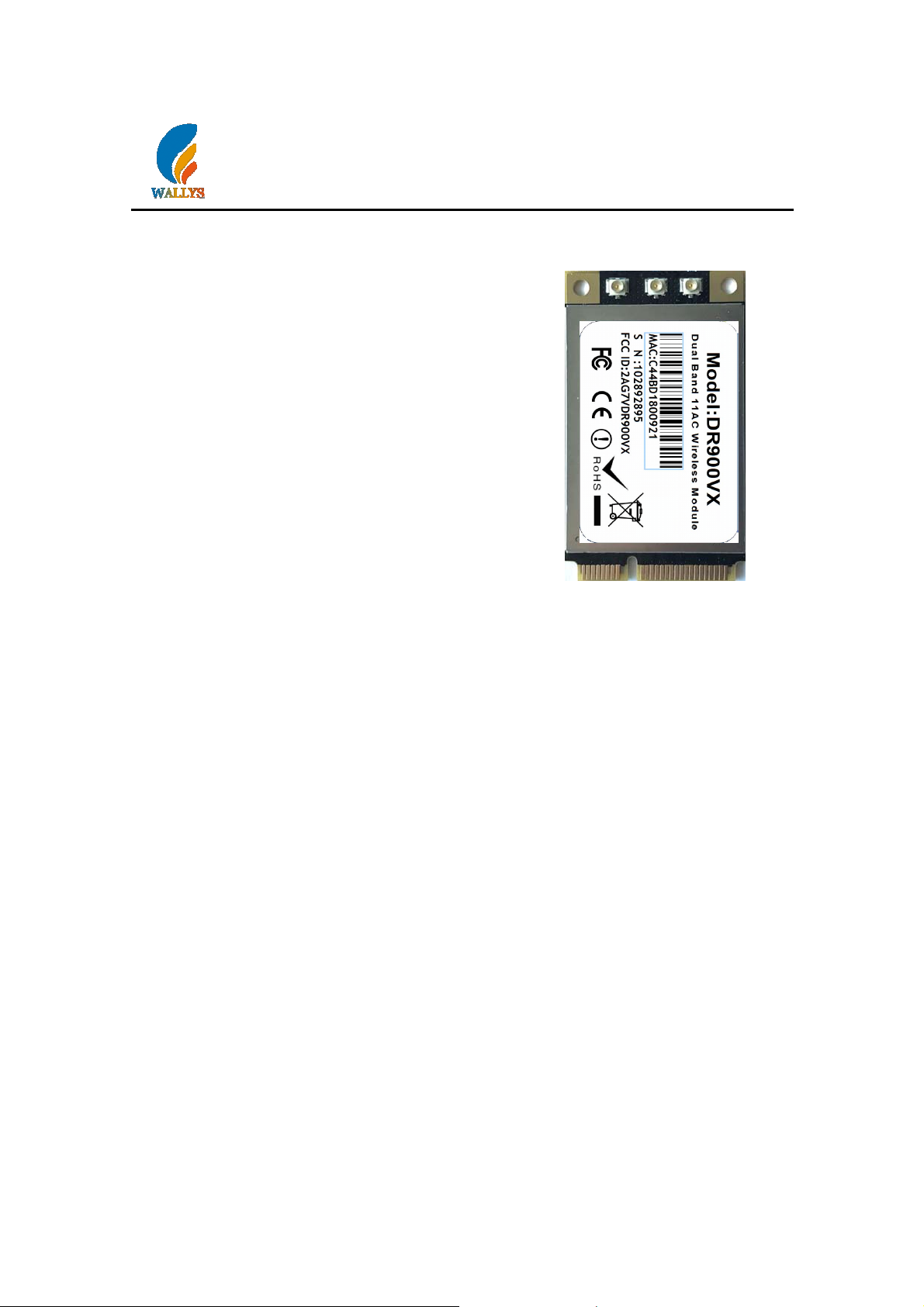
3x3 MIMO 802.11ac Mini PCIe WiFi Module
Dual Band Wireless Access Points
Features
Qualcomm-Atheros QCA9880 chipset
Support 2.4GHz & 5GHz
IEEE 802.11ac compliant & backward compatible with
802.11a/b/g/n
3x3 MIMO Technology, up to 1.3Gbps
Mini PCI Express edge connector
RoHS compliance ensure a high level protection of
human health and the environment from risks that can
be posed by chemicals
Supports Spatial Multiplexing, Cyclic-Delay Diversity
(CDD), Low-Density Parity Check (LDPC) Codes,
DR900VX
Maximal Ratio Combining (MRC), Space Time Block Code (STBC)
Supports IEEE 802.11d, e, h, i, k, r, v time stamp, and w standards
Cards are individually calibrated for Quality Assurance
Applications
Security Surveillance
Commercial radio coverage
Hotel Wireless application
Country coverage
Forest fire protection engineering
Some special
scene application
Product Description
DR900VX based on QCA9880 chipset is an enterprise wireless module integrated with 3x3 5G
high power Radio module and 3x3 2.4G high power Radio module designed specifically to
provide users with mobile access to high-bandwidth video streaming, voice, and data
transmission for office and challenging RF environment in factories, warehouses establishment.
Specifications
http://www.wallystech.com/
1

Symbol Parameter
Chipset QCA9880
Host Interface Mini PCI Express 1.1 Standard
Antenna Connector 3 x UF.L
Frequency Range
Operating Voltage 3.3V DC
Power Consumption
Modulation Techniques
Environmental
Temperature
Environmental Humidity,
non-condensing
ROHS Compliance YES
Dimensions (W×H×D) 30.0mm × 50.9mm × 3.2mm
2.4GHz: 2412 ~ 2462MHz
5GHz:4940~4990MHz、5150~5250MHz、5725~ 5850MHz
OFDM: BPSK, QPSK, DBPSK, DQPSK, 16-QAM, 64-QAM,
256-QAM
Operating: -40°C to 70°C, Storage: -40°C to 90°C
Operating: 5% to 95%, Storage: Max. 90%
http://www.wallystech.com/
2
RF Performance Table
Operating
Mode
2.4 GHz
802.11b
2.4 GHz
802.11g
2.4 GHz
802.11n HT20
2.4 GHz
802.11n HT40
Operating
Mode
2.4 GHz
802.11b
2.4 GHz
802.11g
Data Rate
1Mbps
6Mbps
MCS0
MCS0
Data Rate
s -95dBm
1Mbp
s -94dBm
6Mbp
Max Tune-up Output Power
1 Chain 3 Chains
25.00dBm
23.50dBm
/
/
RX Sensitivity
28.00dBm
24.50dBm
±2dB
/
/
Tolerance
±2dB
2.4 GHz
802.11n HT20
2.4 GHz
802.11n HT40
Operating
Mode
4.9 GHz
Operating
Mode
4.9 GHz
MCS0
MCS0
Data Rate
6Mbp
s
Data Rate
6Mbp
s -94dBm
-93dBm
-92dBm
M
ax Tune-up Output Power
1 Chain 3 Chains
/
RX Sensitivity
22.
50dBm
±2dB
±2dB
http://www.wallystech.com/
3

Operating
Mode
Data Rate
Max Tune-up Output Power
1 Chain 3 Chains
5 GHz(5150-5250MHz)
802.11a
5GHz(5150-5250MHz)
802.11n/ac HT20
5GHz(5150-5250MHz)
802.11n/ac HT40
5 GHz(5150-5250MHz)
802.11ac 80
Operating
Mode
5 GHz(5725-5850MHz)
802.11a
5GHz
(5725-5850MHz)
802.11n/ac HT20
5GHz
(5725-5850MHz)
802.11n/ac HT40
5 GHz(
5725-5850MHz)
80
2.11ac 80
s
6Mbp
MCS0
MCS0
MCS0
Data Rate
s
6Mbp
MCS0
MCS0
MCS0
17.50dBm /
/
/
/
Max Tun
21.00dBm
17.00dBm
15.00dBm
e-up Output Power
1 Chain 3 Chains
20.50dBm /
/
/
/
24.00dBm
23.00dBm
23.00dBm
GPIO Pin Mapping
GPIO Pin Function
GPIO0 WLAN_DIS
GPIO1 WLAN_LED
GPIO2 MCI_CLK_IN
GPIO3 MCI_CLK_OUT
GPIO4 MCI_DATA_OUT
GPIO5 MCI_DATA_IN
GPIO12 TMS
13 TCK
14 TDI
15 TDO
16 CPU_WARM_RESET / JTEG RESET
17 GPIO17_BT_LED
19 ANT_A
20 ANT_B
21 FEM_BS
22 FEM_MODE
http://www.wallystech.com/
4

MiniPCIe Slot Pin Assignment
TOP Side Bottom Side
1 PCIE_WAKE_L 2 VCC_3V3
3 NC 4 GND
5 NC 6 NC
7 PCIE_CLKREQ_L 8 NC
9 GND 10 NC
11 PCIE_REFCLK_N 12 NC
13 PCIE_REFCLK_P 14 NC
15 GND 16 NC
Mechanical key
17 NC 18 GND
19 NC 20 GPIO0_WLAN_DIS
21 GND 22 PCIE_RST_L
23 PCIE_TX_N 24 VCC_3V3
25 PCIE_TX_P 26 GND
27 GND 28 NC
29 GND 30 NC
31 PCIE_RX_P 32 NC
33 PCIE_RX_N 34 GND
35 GND 36 NC
37 GND 38 NC
39
41
43 GND 44 GPIO1_WLAN_LED
45 NC 46 GPIO17_BT_LED
47 NC 48 NC
49 NC 50 GND
51 NC 52 VCC_3V3
VCC_3V3
(RESERVED)
VCC_3V3
(RESERVED)
40 GND
42
NC
http://www.wallystech.com/
5

Pin1
1)the picture show us the Pin 1 and the pin51,the pin numbers are increasing by odd
numbers on the top side
2)and increasing by even numbers from Pin2 to Pin52 on the bottom side;the pin2 is on the
bottom of the pin1
;
Pin51
Version
Version CPU Feature
DR900VX QCA9880
DR900VX-MX QCA9880
DR900VX-4.9 QCA9880
DR600VX
DR600VX-MX
DR600VX-4.9
QCA9880
QCA9880
QCA9880
The differences of them
are model names
OEM/Integrators Installation:
1.0 This module has been tested and found to comply with 15.247/15.407/PART90Y
requirements for Modular Approval.
This module can work with 2.4G,4.9G and 5G,but the three band can't work together.
1.1. Summarize the specific operational use conditions
This module can be used in Commercial radio coverage and other equipment. The
input voltage to the module should be nominally 3.3VDC ,the ambient temperature of
the module is -40°~70°.And the antenna needs to be changed, the certification should
be re-applied.
1.2. Limited module procedures
NA
http://www.wallystech.com/
6

1.3. Trace antenna designs
NA
1.4. RF exposure considerations
This equipment complies with FCC radiation exposure limits set forth for an uncontrolled
environment .This equipment should be installed and operated with minimum distance 20cm
between the radiator& your body. If the device built into a host as a portable usage, the
additional RF exposure evaluation may be required as specified by 2.1093.
1.5. Antennas
Antenna type:
External fixed
omni
antenna
2.4GHz band
Peak Gain
2(dBi)
4.9GHz band
Peak Gain
2(dBi)
5150GHz~
5250GHz
Peak
Gain
2dBi)
5725GHz~
5850GHz
Peak Gain
2(dBi)
1.6. Label and compliance information
When the module is installed in the host device, the FCC ID label must be visible through a
window on the final device or it must be visible when an access panel, door or cover is easily
re-moved. If not, a second label must be placed on the outside of the final device that contains
the following text: “Contains FCC ID: 2AG7VDR900VX”. The FCC ID can be used only when
all FCC ID compliance requirements are met.
1.7. Information on test modes and additional testing requirements
a) The modular transmitter has been fully tested by the module grantee on the required
number of channels,modulation types, and modes, it should not be necessary for the host
installer to re-test all the available transmitter modes or settings. It is recommended that the
host product manufacturer, installing the modular transmitter,perform some investigative
measurements to confirm that the resulting composite system does not exceed the spurious
emissions limits or band edge limits (e.g., where a different antenna may be causing additional
emissions).
b) The testing should check for emissions that may occur due to the intermixing of emissions
with the other transmitters, digital circuitry, or due to physical properties of the host product
(enclosure). This investigation is especially important when integrating multiple modular
transmitters where the certification is based on testing each of them in a stand-alone
configuration. It is important to note that host product manufacturers should not assume that
because the modular transmitter is certified that they do not have any responsibility for final
product compliance.
http://www.wallystech.com/
7

c) If the investigation indicates a compliance concern the host product manufacturer is
obligated to mitigate the issue. Ho
st products using a modular transmitter are subject to all the
applicable individual technical rules as well as to the general conditions of operation in
Sections 15.5, 15.15, and 15.29 to not cause interference. The opera tor of the host product will
be obligated to stop operating the device until the interference have been corrected .
1.8. Additional testing, Part 15 Sub part B disclaimer The final host / module combination need
to be evaluated against the FCC Part 15B criteria for unintentional radiators in order to be
properly authorized for operation as a Part 15 digital device.
The host integrator installing this module into their product must ensure that the final
composite product complies with the FCC requirements by a technical assessment or
evaluation to the FCC rules, including the transmitter operation and should refer to guidance in
KDB 996369. For host products with certified modular transmitter, the frequency range of
investigation of the composite system is specified by rule in Sections 15.33(a)(1) through
(a)(3), or the range applicable to the digital device, as shown in Section 15.33(b)(1), whichever
is the higher frequency range of investigation When testing the host product, all the
transmitters must be operating.The transmitters can be enabled by using publicly-available
drivers and turned on, so the transmitters are active. In certain conditions it might be
appropriate to use a technology-specific call box (test set) where accessory 50 devices or
drivers are not available. When testing for emissions from the unintentional radiator, the
transmitter shall be placed in the receive mode or idle mode, if possible. If receive mode only is
not possible then, the radio shall be passive (preferred) and/or active scanning. In these cases,
this would need to enable activity on the communication BUS (i.e., PCIe, SDIO, USB) to
ensure the unintentional radiator circuitry is enabled. Testing laboratories may need to add
attenuation or filters depending on the signal strength of any active beacons (if applicable)
from the enabled radio(s). See ANSI C63.4, ANSI C63.10 and ANSI C63.26 for further general
testing details.
The product under test is set into a link/association with a partnering WLAN device, as per the
normal intended use of the product. To ease testing, the product under test is set to transmit at
a high duty cycle, such as by sending a file or streaming some media content.
FCC Statment:
Changes or modifications not expressly approved by the party responsible for
Any
complianc
e could
void the user's
authority to operate the equipment.
This device complies with part 15 of the FCC Rules . Operation is subject tn the fol lowing
two conditions:
(1) This device may not cause harmful interference, and
(2) This device must accept any interference received, including interference that may
cause undesired operation.
http://www.wallystech.com/
8
 Loading...